

Page 1

IF Down Converter for Digital Broadcast
Description
The CXA3556N is a one-chip integrated IC that
processes IF signals of a digital broadcast tuner and
includes an AGC amplifier circuit, a mixer circuit, a
local oscillator circuit and an output amplifier circuit.
The package utilizes a 24-pin SSOP suitable for
surface mounting.
Features
• AGC control width that has a 56dB variable range
• Low noise characteristics
• Low distortion characteristics (in par ticular, during
AGC gain reduction)
• Includes switching function between down
converter mode and linear amplifier mode
• Variable output amplifier gain by changing external
resistance
• Includes RF AGC output pin
• Variable RF AGC settings
• AGC control curve characteristics with excellent
linearity
Absolute Maximum Rating (Ta = 25°C)
• Supply voltage Vcc –0.3 to +12 V
• Operating temperature Topr –55 to +150 °C
Operating Conditions
• Supply voltage Vcc 4.75 to 5.25 V
• Operating temperature Topr –25 to +75 °C
CXA3556N
24 pin SSOP (Plastic)
Applications
Digital broadcast tuners
Structure
Bipolar silicon monolithic IC
Sony reserves the right to change products and specifications without prior notice. This information does not convey any license by
any implication or otherwise under any patents or other right. Application circuits shown, if any, are typical examples illustrating the
operation of the devices. Sony cannot assume responsibility for any problems arising out of the use of these circuits.
– 1 –
E02426-PS
Page 2
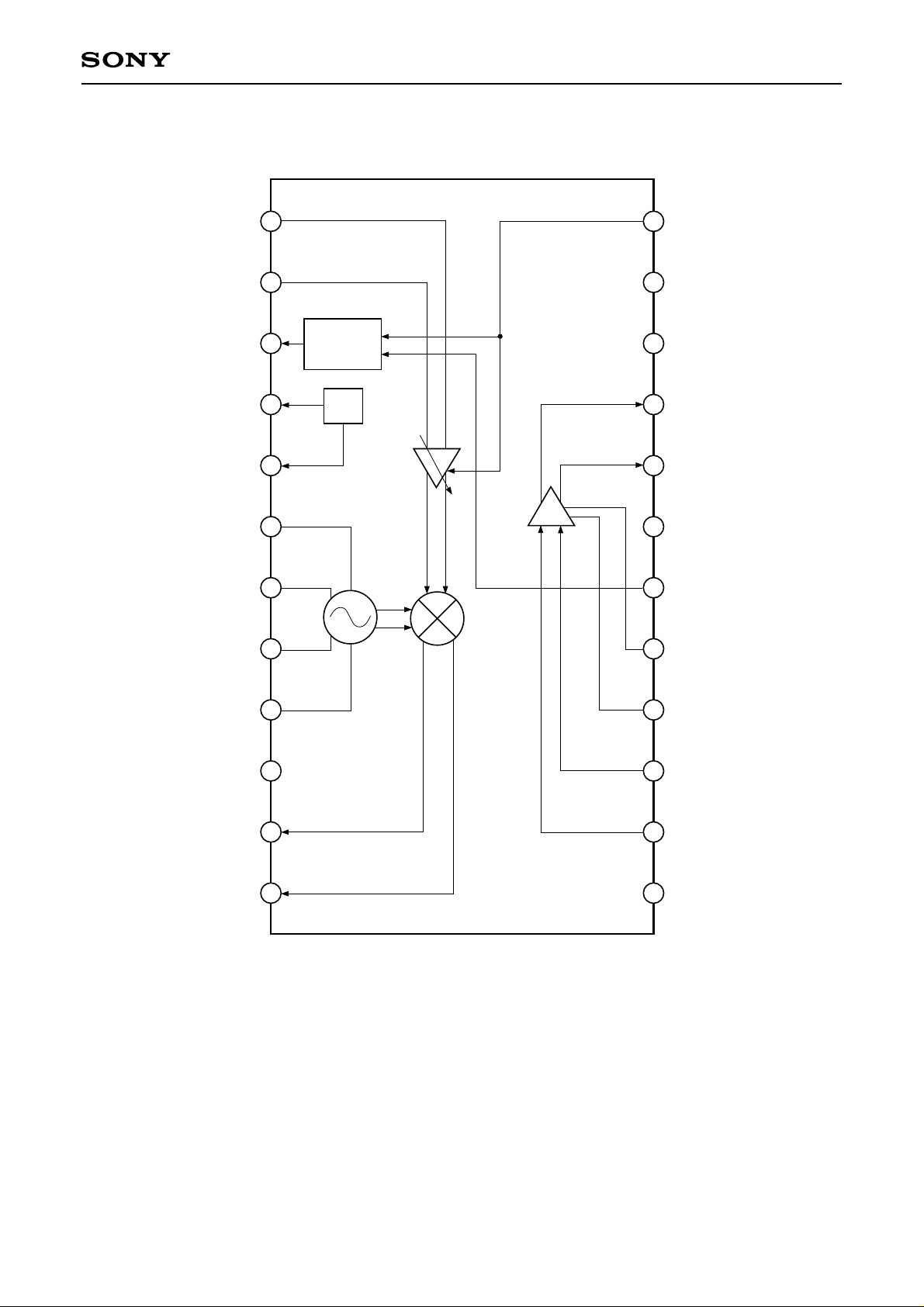
Block Diagram and Pin Configuration
CXA3556N
IFIN1
IFIN2
RFAGC
IREG
VREG
LOB1
LOC1
LOC2
1
2
3
4
5
6
7
8
Comparator
REG
OSC
AGC
Amp.
Mixer
Output
Amp.
AGCIN
24
MODESEL
23
AGCGND
22
AO2
21
AO1
20
GND
19
AGCREF
18
17
E2
LOB2
CC
V
MO1
MO2
9
10
1
11
12
16
15
14
13
E1
AIN2
AIN1
CC
V
2
– 2 –
Page 3
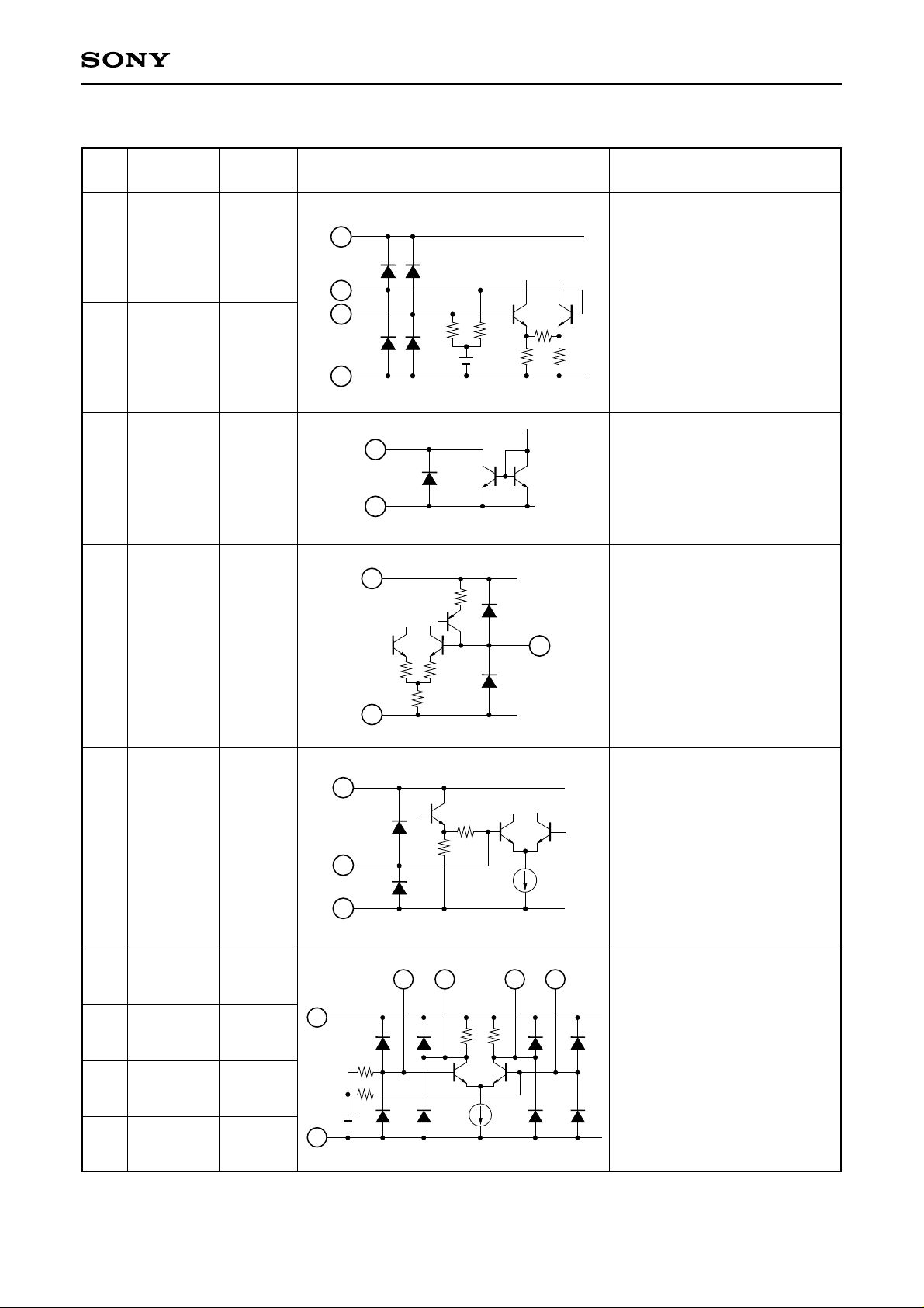
Pin Description and Equivalent Circuit
CXA3556N
Pin
No.
Symbol
Pin
voltage
1 IFIN1 1.4V
2 IFIN2 1.4V
3 RFAGC —
10
22
Equivalent circuit Pin description
CC
1
V
1
2
5k
3
5k
AGCGND
IF inputs.
RF AGC voltage output.
Comparator output.
Low level: 0.4V or less
High level: 8V or more
10
22
AGCGND
V
CC1
4 IREG 2.6V
5VREG 3.3V
6 LOB1 2.9V
7 LOC1 3.7V
8 LOC2 3.7V
10
10
22
Connects external resistance
27kΩ.
22
AGCGND
4
V
CC
1
Connects external capacitance
5
AGCGND
6
978
1µF.
V
CC
1
Connects external capacitance
and crystal oscillator.
9 LOB2 2.9V
19
GND
– 3 –
Page 4
CXA3556N
Pin
No.
Symbol
10 VCC15V
Pin
voltage
Equivalent circuit Pin description
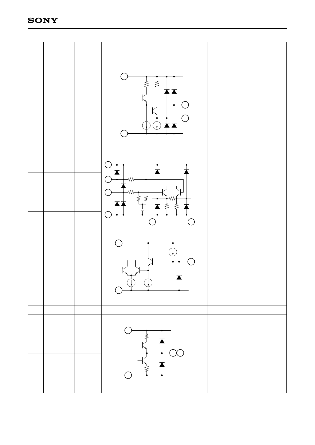
Power supply.
V
CC
10
1
11 MO1 2.3V
11
12
Mixer output pin.
12 MO2 2.3V
19
GND
13 VCC2 5V Power supply.
CC
1
14 AIN1 1.3V
15 AIN2 1.3V
16 E1 0.6V
10
14
15
200
200
10k
10k
V
Output amplifier circuit inputs.
Gain of output amplifier circuit
can be changed by connecting
external resistance between
Pins 16 and 17.
17 E2 0.6V
18 AGCREF —
19
10
17 16
V
90µA
CC1
18
GND
RF AGC setting voltage
adjustment pin.
Connect external resistance
between Pin 18 and GND and
change the value to change
RF AGC output voltage.
22
AGCGND
19 GND 0V GND
CC
1
V
20 21
Output amplifier output.
20 AO1 2.7V
10
21 AO2 2.7V
19
GND
– 4 –
Page 5
CXA3556N
Pin
No.
Symbol
Pin
voltage
Equivalent circuit Pin description
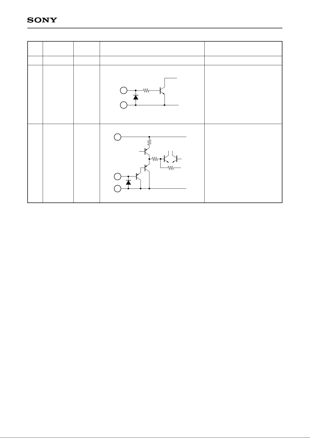
22 AGCGND 0V AGC circuit GND.
Selects either IF down
converter mode or linear
23
20k
23 MODESEL —
amplifier mode.
When the voltage applied to
this pin is 0.3V or less, the
mode is down converter mode.
22
GND
When the voltage is 4.75 to
5.25V, the mode is linear
amplifier mode.
V
CC
10
24 AGCIN —
24
22
1
AGC control.
Input voltage range is 0 to 2.2V.
AGCGND
– 5 –
Page 6

Electrical Characteristics (VCC = 5V, Ta = 25°C)
(1) IF down converter mode (fvco = 49.38MHz)
CXA3556N
Item
Current
consumption A
Gain 1
Gain 2
Gain width
IM3_1
IM3_2
Output noise 1
Output noise 2
Symbol
ICCA
G1
G2
G3
DIS1
DIS2
NF1
NF2
(2) Linear amplifier mode
Item
Symbol
Measurement conditions
Input signal = no signal
AGC_IN voltage = 0V
Input signal = 1 wave (43.5MHz), AGC_IN voltage = 2.2V
Output signal = 1Vp-p
Input signal = 1 wave (43.5MHz), AGC_IN voltage = 0V
Output signal = 1Vp-p
G3 = G1 – G2
Input signal = 2 waves (43.5MHz, 43.6MHz)/–26dBm
Output signal = 1Vp-p
Input signal = 2 waves (43.5MHz, 43.6MHz)/–21dBm
Output signal = 1Vp-p
Input signal = –60dBm (43.5MHz)
Output signal = 1Vp-p
Input signal = –20dBm (43.5MHz)
Output signal = 1Vp-p
Measurement conditions
Min. Typ.
63
44
68.5
65
12.2
10
56
54
–51
–44
–51
–42
–100
—
–120
—
Min. Typ.
77
73
15
58
—
—
–96
Unit
mA
dB
dB
dB
dBc
dBc
dBc/Hz
dBc/Hz
Max.
–111
Max. Unit
Current
consumption B
Gain 4
Gain 5
Gain width
IM3_3
IM3_4
Output noise 3
Output noise 4
ICCB
G4
G5
G6
DIS3
DIS4
NF3
NF4
Input signal = no signal
AGC_IN voltage = 0V
Input signal = 1 wave (43.5MHz), AGC_IN voltage = 2.2V
Output signal = 1Vp-p
Input signal = 1 wave (43.5MHz), AGC_IN voltage = 0V
Output signal = 1Vp-p
G6 = G4 – G5
Input signal = 2 waves (43.5MHz, 43.6MHz)/–26dBm
Output signal = 1Vp-p
Input signal = 2 waves (43.5MHz, 43.6MHz)/–21dBm
Output signal = 1Vp-p
Input signal = –60dBm (43.5MHz)
Output signal = 1Vp-p
Input signal = –20dBm (43.5MHz)
Output signal = 1Vp-p
(3) Output amplifier characteristics
Item
F
characteristics
Symbol
F
Input signal = 60MHz
Short between Pins 16 and 17
Measurement conditions
63
44
68.5
65
12.7
10
56
54
–51
–44
–51
–42
–100
—
–120
—
Min. Typ.
–1.5
mA
77
dB
73
dB
15
dB
58
dBc
—
dBc
—
dBc/Hz
–96
dBc/Hz
–111
Max. Unit
dB0–3
– 6 –
Page 7
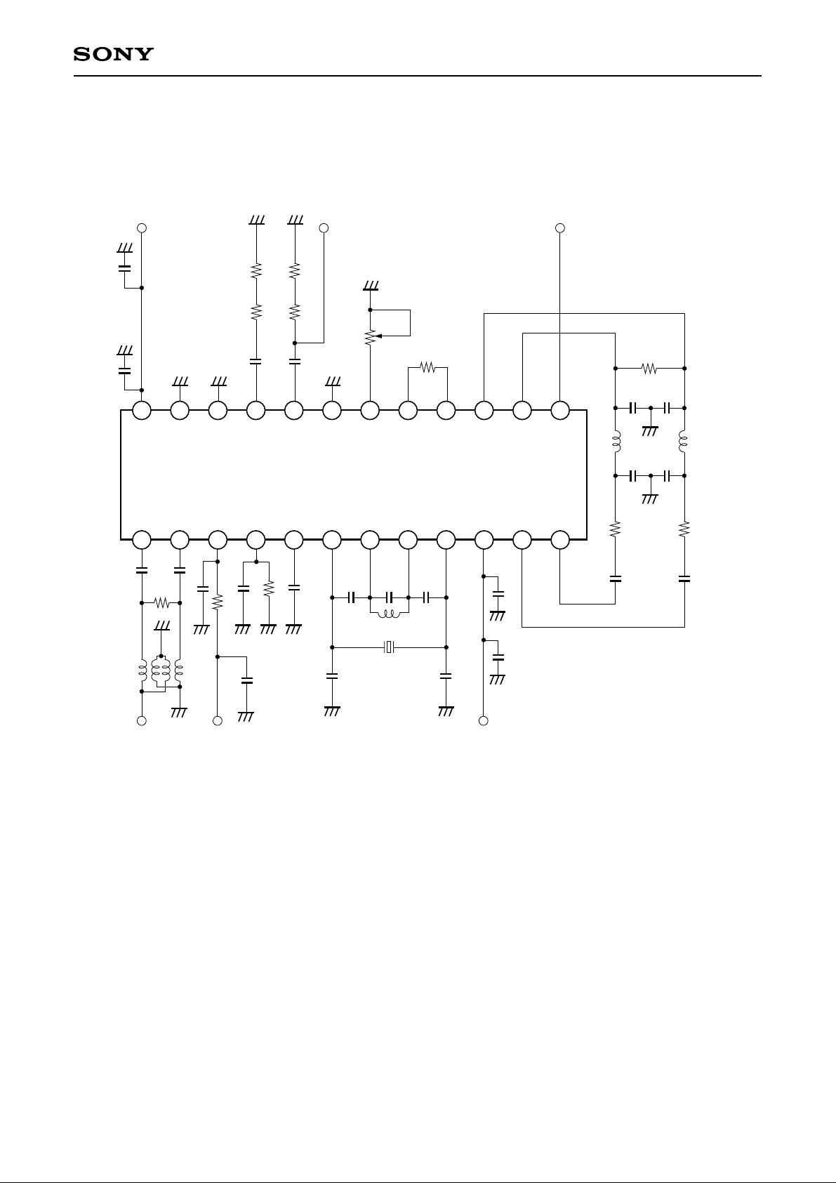
Measurement circuit 1
IF down converter mode
AGCIN
0 to 2.2V
Output
5V (I
CXA3556N
∗
3
CC
2)
1µ
1n
AGCIN
IFIN1
1n 1n
200
1
∗
SG input 9V
AGCGND
MODESEL
IFIN2
RFAGC
1n
1n
47k
51
51
470
470
10n
R
10n
1k
2124 23 22 20 19 18 17 16 15 14 13
E2
AO2
AO1
GND
E1
AIN2
AGCREF
1
IREG
VREG
LOB1
LOC1
LOC2
LOB2
CC
V
41 2 3 5 6 7 8 9 10 11 12
27k
1µ
2p 10p
2p
100p
1µH
100p
1µ
49.38MHz
2
∗
27p 27p
5V (ICC1)
∗
3
680
51p 51p
2
AIN1
MO1
CC
V
MO2
6.8µH
51p
300 300
6.8µH
51p
10n 10n
∗
1
Toko 617DB-1018
∗
2
3rd overtone crystal oscillator (49.381MHz)
∗
3
ICCA = ICC1 + ICC2
– 7 –
Page 8

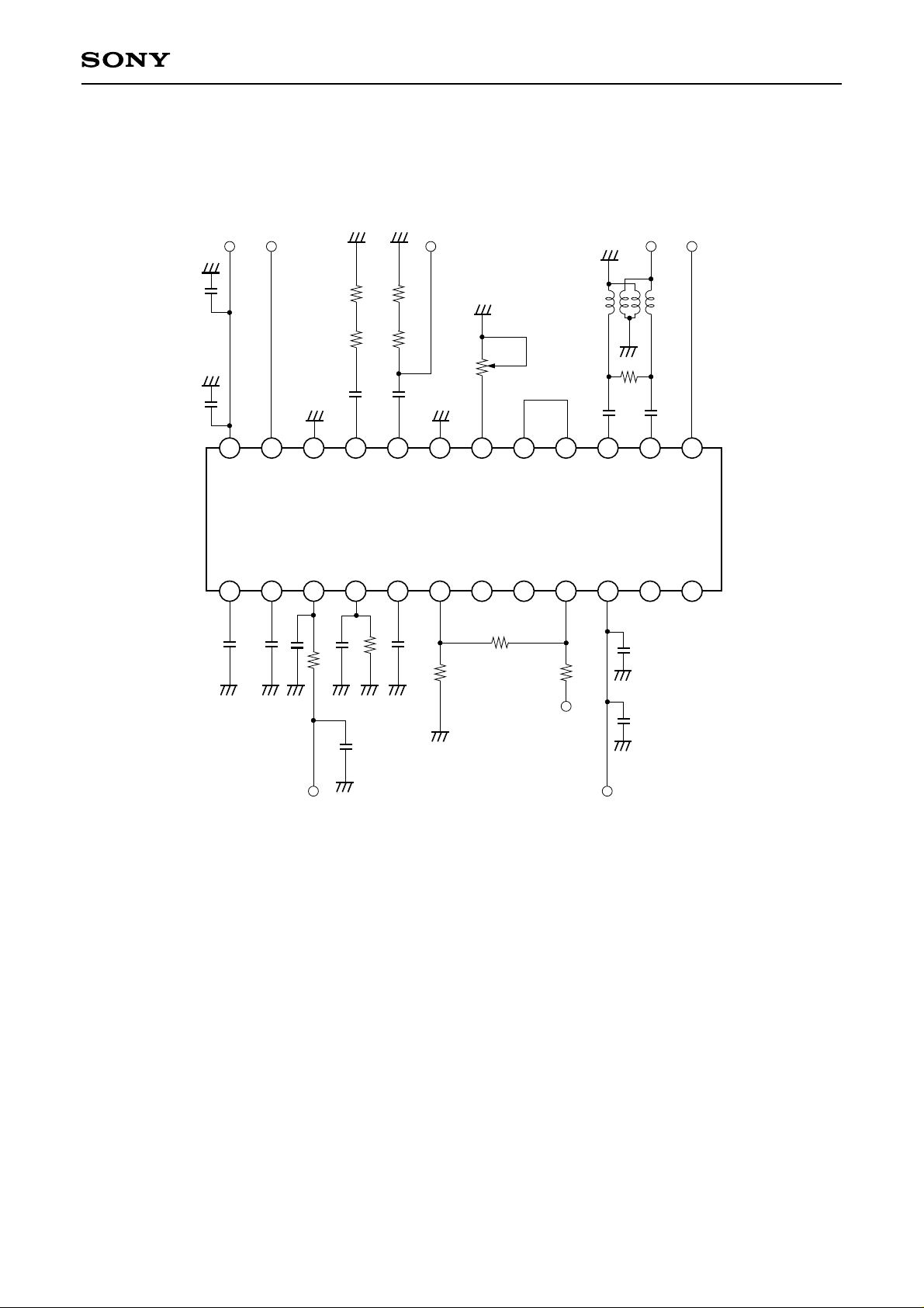
Measurement circuit 2
Linear mode
AGCIN
0 to 2.2V 5V (I
CC
CXA3556N
∗
4
1)
Output
5V (I
CC
2)
1µ
1n
AGCIN
IFIN1
1n 1n
200
AGCGND
MODESEL
IFIN2
RFAGC
1n
1n
47k
51
51
470
470
R
1n
1n
2124 23 22 20 19 18 17 16 15 14 13
E2
AO2
AO1
GND
E1
AIN2
AGCREF
1
IREG
VREG
LOB1
LOC1
LOC2
LOB2
CC
V
41 2 3 5 6 7 8 9 10 11 12
27k
100p
1µ
1k
5V
2k
100p
2k
1µ
AIN1
MO1
2
CC
V
MO2
∗
4
680
300 300
1n 1n
ICCB = ICC1 + ICC2
SG input 9V
– 8 –
5V (ICC1)
4
∗
Page 9
Measurement circuit 3
Output amplifier F characteristics
CXA3556N
AGCIN
0 to 2.2V 5V (I
1µ
1n
AGCIN
IFIN1
1n
1n
CC
2)
AGCGND
MODESEL
IFIN2
RFAGC
1n
1n
47k
51
470
470
1n
Output
51
50k
1n
IF input
∗
1
200
2124 23 22 20 19 18 17 16 15 14 13
E2
AO2
AO1
GND
E1
AIN2
AGCREF
1
IREG
VREG
LOB1
LOC1
LOC2
LOB2
CC
V
41 2 3 5 6 7 8 9 10 11 12
27k
100p
1µ
1k
2k
2k
1n1n
AIN1
MO1
5V (I
CC
2
CC
V
MO2
2)
5V
1µ
9V 5V (ICC1)
100p
– 9 –
Page 10
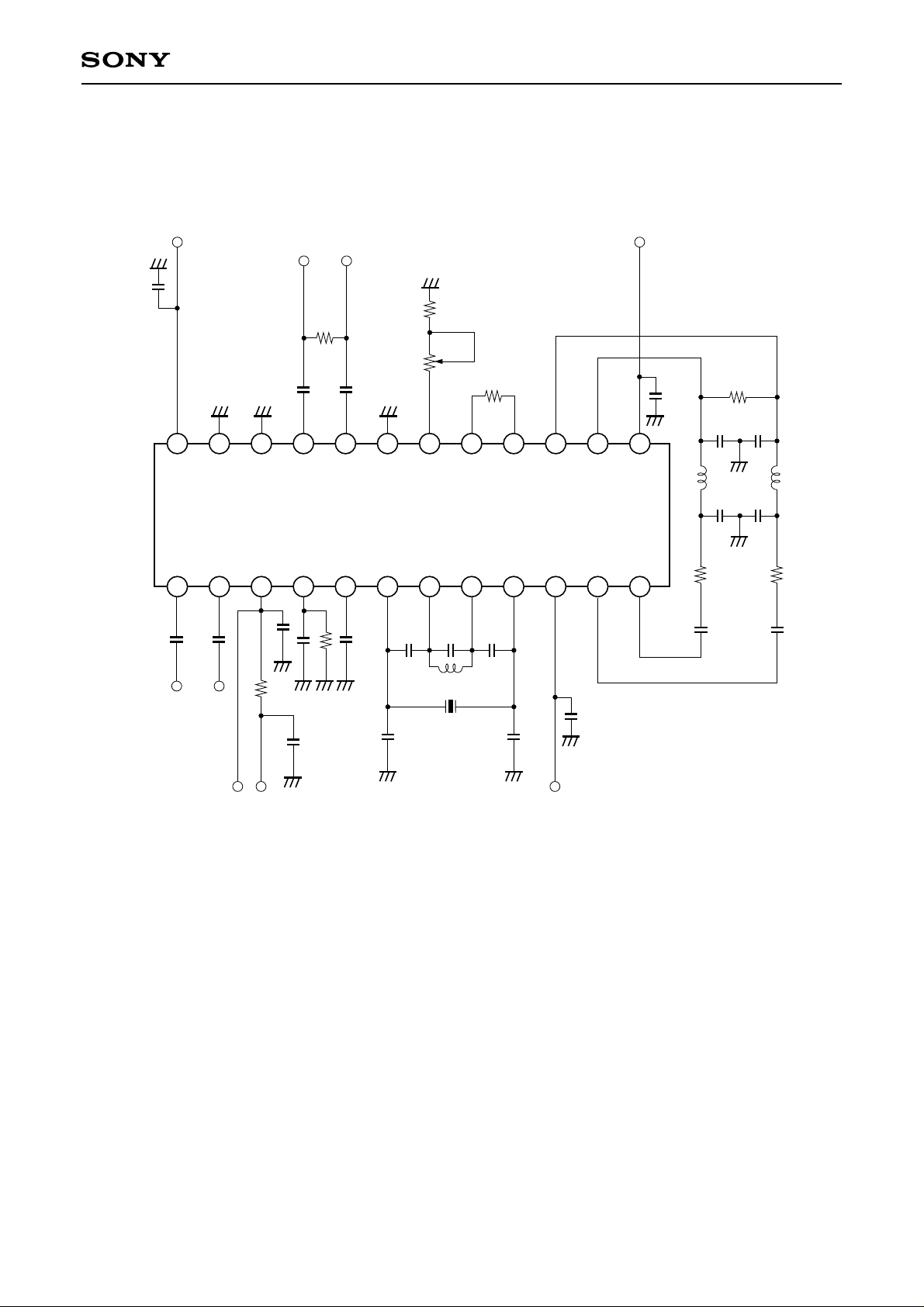
Application circuit
IF down converter mode
CXA3556N
1µ
AGCIN
0 to 2.2V
AGCIN
IFIN1
1n1n
AGCGND
MODESEL
IFIN2
RFAGC
1n
Output
GND
LOB1
2p 10p
27k
10k
AGCREF
LOC1
1k
E2
LOC2
2p
E1
LOB2
AIN2
CC1
V
AIN1
MO1
1k
10n
10n
2124 23 22 20 19 18 17 16 15 14 13
AO2
AO1
IREG
VREG
41 2 3 5 6 7 8 9 10 11 12
27k
1n
1µ
V
CC
680
47p 47p
6.8µH
47p
330 330
10n 10n
6.8µH
47p
CC2
V
MO2
1µ
1µH
IF input
Application circuits shown are typical examples illustrating the operation of the devices. Sony cannot assume responsibility for
any problems arising out of the use of these circuits or for any infringement of third party patent and other right due to same.
47k
49.38MHz
27p 27p
1µ
9VRFAGC
∗2
1µ
VCC
– 10 –
Page 11

CXA3556N
Description of Functions
The CXA3556N is an IF down converter IC for digital broadcasts. This IC contains a mixer circuit, a local
oscillator circuit and an AGC circuit that standardizes IF signals in response to levels of input signals.
It can also operate in a mode other than down converter (linear amplifier mode) and making possible use in a
wide variety of digital broadcast tuners. (Control using Pin 23 bias voltage.)
1. AGC Circuit
This is a variable gain amplifier circuit that standardizes output in response to levels of input signals. This
circuit has especially excellent low distortion and noise characteristics even when the input level is large. It
also has a variable width of 56dB as the gain control range with excellent linearity of the gain control curve.
2. Local Oscillator Circuit
This circuit has a structure that uses a crystal oscillator and oscillates at 3rd overtone frequency. The circuit
sets the parallel frequency of the parallel LC resonator between Pins 7 and 8 close to a tertiary overtone
frequency (FVCO). This oscillator circuit can also use an LC resonance circuit in place of the crystal oscillator
to form an oscillator circuit.
3. Output Amplifier Circuit
Adding a resistor between Pins 16 and 17 allows the gain to be changed in proportion to that resistance.
(Refer to characteristic graph Fig. 5 Gain vs. resistance between E1 and E2.)
The output stage of this amplifier is also designed to be 500Ω load/1Vp-p.
4. Mixer Circuit
This circuit outputs the frequency difference between the signal input to IF IN and the local oscillator signal.
5. RF AGC Circuit
This circuit has high image quality in both strong and weak electric fields. In particular, it controls the RF IC
gain existing in the first stage of the CXA3556N to delay the characteristics related to S/N to the maximum
limits. The circuit controls the RF IC gain using RF AGC voltage (Pin 3) in order that signals input to IF IN
(Pins 1, 2) grow larger in weak electric fields. The RF AGC voltage at Pin 3 is obtained from results of a
comparison between the AGC control voltage (Pin 24 input voltage) that detects output signals and the
voltage at Pin 18 that can be freely set using the resistance value. When the control voltage is low, the RF IC
gain decreases and when the control voltage is high, the RF IC gain increases.
– 11 –
Page 12

IF down converter mode characteristics
Fig. 1. Gain vs. AGCIN voltage Fig. 2. Output noise vs. input level
80
CXA3556N
–60
70
60
50
40
Gain [dB]
30
20
10
0
0 0.2 0.4 0.6 0.8 1.0 1.2
Fig. 3. IM3 vs. input level Fig. 4. REFAGC voltage vs. AGCIN voltage
0
–10
–20
–30
–40
IM3 [dBc]
–50
–60
–70
–70 –60 –50
1.4 1.6 1.8 2.0 2.2
AGCIN voltage [V]
–40 –30 –20 –10 0
Input level [dBm]
–70
–80
–90
–100
–110
Output noise [dBc/Hz]
–120
–130
–70 –60 –50
10
9
8
7
6
5
4
3
REFAGC voltage [V]
2
1
0
0.5 0.6 0.7 0.8 0.9 1.0 1.1 1.2
–40 –30 –20 –10 0
Input level [dBm]
AGCIN voltage [V]
R = 30kΩ
1.3 1.4 1.5
Fig. 5. Gain vs. resistance between E1 and E2 Fig. 6. Input characteristics
16
14
12
10
8
6
Gain [dB]
4
2
0
–2
–4
1 10 100 1000 10000 100000 1E+06
Resistance between E1 and E2 [Ω]
∗
Gain when 1kΩ is connected between E1 and E2 is 0dB.
70MHz 109Ω –625Ω 3.6pF
30MHz 488.44Ω –1.3237kΩ 4.0079pF
0
–j25
Start 30MHz Stop 70MHz
j50
50
–j50
– 12 –
j100j25
30MHz
70MHz
–j100
Page 13
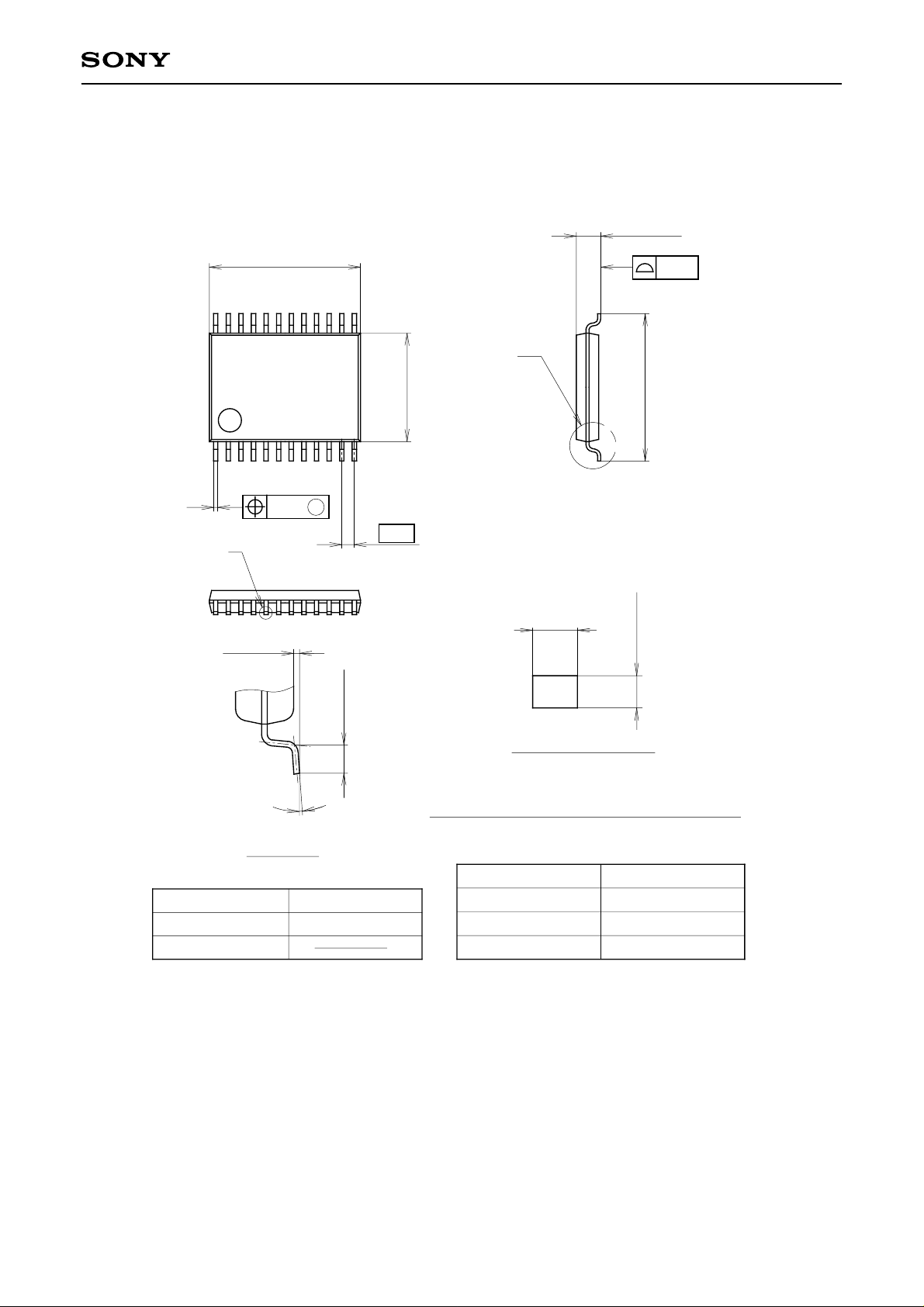
Package Outline Unit: mm
CXA3556N
b
24
1
B
0.1 ± 0.1
∗7.8 ± 0.1
0.13
24PIN SSOP (PLASTIC)
13
∗5.6 ± 0.1
12
M
0.65
A
b=0.22 ± 0.03
+ 0.2
1.25 – 0.1
7.6 ± 0.2
+ 0.03
0.15 – 0.01
0.1
SONY CODE
EIAJ CODE
JEDEC CODE
0˚ to 10˚
DETAIL
0.5 ± 0.2
A
SSOP-24P-L01
P-SSOP24-7.8x5.6-0.65
DETAIL B : PALLADIUM
NOTE: Dimension "∗" does not include mold protrusion.
PACKAGE STRUCTURE
PACKAGE MATERIAL
LEAD TREA TMENT
LEAD MATERIAL
PACKAGE MASS
EPOXY RESIN
PALLADIUM PLATING
COPPER ALLOY
0.1g
– 13 –
Sony Corporation
 Loading...