

Page 1

Description
The CXA3512R is a driver IC for the analog inputs
of SVGA or higher Sony polycrystalline silicon TFT
LCD panels. It has a line invert amplifier and analog
demultiplexers, as well as the timing generator and
output buffers required for these. The CXA3512R
can directly drive an LCD panel. The VCOM setting
circuit and precharge pulse waveform generator are
also on-chip.
Features
• High-speed signal processing supports XGA high refresh signal
• Overall wide band response
• Low output deviation by on-chip output offset cancel circuit
• Invert amplifier with small phase delay difference between inverted signal and non-inverted signal
• On-chip timing generator with ECL
• Dot clock phase adjustment function
• VCOM voltage generation circuit
• Precharge pulse waveform generation circuit
Absolute Maximum Ratings
• Supply voltage Vcc 16 V
VDD 5.5 V
• Operating temperature –20 to +70 °C
• Storage temperature –65 to +150 °C
• Allowable power dissipation PD 2300 mW (single layered board mounted)
Recommended Operating Conditions
• Supply voltage Vcc 15.0 to 15.5 V
VDD 4.75 to 5.25 V
• Ambient temperature –20 to +70 °C
LCD Driver
– 1 –
E99803A9Z-PS
Sony reserves the right to change products and specifications without prior notice. This information does not convey any license by
any implication or otherwise under any patents or other right. Application circuits shown, if any, are typical examples illustrating the
operation of the devices. Sony cannot assume responsibility for any problems arising out of the use of these circuits.
CXA3512R
64 pin LQFP (Plastic)
For the availability of this product, please contact the sales office.
Page 2

– 2 –
CXA3512R
Block Diagram
S/H S/H S/H
VCOM
OFFSET CANCEL
BUFFER
S/H S/H S/H
OFFSET CANCEL
BUFFER
S/H S/H S/H
OFFSET CANCEL
BUFFER
S/H S/H S/H
OFFSET CANCEL
BUFFER
S/H S/H S/H
OFFSET CANCEL
BUFFER
S/H S/H S/H
OFFSET CANCEL
BUFFER
1 2 3 4 5 6 7 8 9 10 11 12 13 14 15 16
17
18
19
20
21
22
23
24
25
26
27
28
29
30
31
32
33343536373839404142434445464748
49
50
51
52
53
54
55
56
57
58
59
60
61
62
63
64
CAL_R
CAL_O
CAL_I
V
DD
DGND
MCLK
MCLKX
GND
GND
DLYCTR
CLKOUT
CLKOUTX
NC
CLKIN
CLKINX
F/H_CNT
PRGPOL
PRG
NC
NC
POSCTR1
POSCTR2
NC
GND
GND
STATUS
ENB
D1OR2
DIRCTR
NC
NC
DCFBSW
NC
VIDEO_I
VIDEO_R
VIDEO_O
SH_IN
NC
VCCGND
GND
SID_IN
SID_R
SID_O
FRP
SIGCNT
VCOMOFF
VCOMOUT
SHOUT1
NC
SHOUT2
NC
SHOUT3
NC
PV
CC
GND
GND
PGND
NC
SHOUT4
NC
SHOUT5
NC
SHOUT6
D
CLOCK
DELAY
S/H
pulses
TIMING
GENERATOR
offset
cancel
mode
timing
SID
INVERT
AMP
CALIBRATION
AMP
Page 3

– 3 –
CXA3512R
Pin Description
Pin
No.
Symbol I/O
Standard
voltage level
Equivalent circuit
Description
1 PRGPOL
I
High: ≥ 2.5V
Low: ≤ 0.8V
OPEN High
Selects the latch polarity of the PRG
pulse used as the time reference.
High: PRG pulse is latched at the
falling edge of CLKIN.
Low: PRG pulse is latched at the
rising edge of CLKIN.
Select the polarity with sufficient
timing margin after adjusting the
analog video and CLKIN phases
with DLYCTR.
1
VDD
40k
100k
20k
12µ
20k
VDD
VDD VDD
2
PRG I
High: ≥ 2.5V
Low: ≤ 0.8V
PRG pulse input.
See the Timing Chart.
2
VDD
VDD
145
50k
150k
VDD
50k
5
6
POSCTR1
POSCTR2
I
See Table
A-1.
Output phase adjustment.
Each pin has 4 setting values, for a
total of 16 settings.
(Adjustment in 1 dot clock units in
XGA mode, 1/2 dot clock units in
SVGA mode, and 1 dot clock units in
SXGA mode.)
See Tables A-1, A-2 and A-3.
5
6
VDD
60k
2k
VDD
10 STATUS
I
High: ≥ 2.5V
Low: ≤ 0.8V
OPEN High
Used in XGA and UXGA modes
(when using 2 ICs for a gammacorrected IC).
During forward scan, high: 2nd
device, low: 1st device
During reverse scan, high: 1st
device, low: 2nd device
See Table B.
10
VDD
40k
100k
20k
12µ
20k
VDD
VDD VDD
11
ENB
I
High: ≥ 2.5V
Low: ≤ 0.8V
ENB pulse input.
See the Timing Chart.
11
VDD
VDD
145
50k
150k
VDD
50k
13 D1OR2 I
High: ≥ 2.5V
Low: ≤ 0.8V
OPEN High
CLKOUT pin frequency selection.
High: same frequency as MCLK
Low: double the MCLK frequency
13
VDD
40k
100k
20k
12µ
20k
VDD
VDD VDD
Page 4

– 4 –
CXA3512R
14 DIRCTR
I
High: ≥ 2.5V
Low: ≤ 0.8V
OPEN High
Scan direction setting.
Low: output as a time series in
descending order (reverse scan) of
output pin symbol (in order from
SHOUT6 to SHOUT1)
High: output in ascending order
(forward scan)
14
VDD
40k
100k
20k
12µ
20k
VDD
VDD VDD
16 DCFBSW
I
OPEN High
Offset cancel circuit on/off switch.
High: cancel circuit on
Use this pin at on (open).
16
VDD
40k
100k
10µ
VDD
VDD
40k
17
19
21
28
30
32
SHOUT6
SHOUT5
SHOUT4
SHOUT3
SHOUT2
SHOUT1
O
1.5 to 13.5V
Demultiplexer outputs.
Can be connected directly to the
LCD input pins.
30
32
28
19
21
17
VCC
VCC
VCC
300
300
33 VCOMOUT
O
3 to 7V
LCD common voltage of panel
output.
Can be set to VSIGCNT to
(VSIGCNT – 3V) by the Pin 34 input.
70µ
VCC
33
VCC
145 60k
500
VCC
500
34 VCOMOFF
I
0 to 10V
VCOMOUT (Pin 33) voltage setting.
VCOMOUT is the same potential as
SIGCNT for input of 0V, and
approximately 3V lower than that for
input of 10V.
34
VCC
2k
100k
60µ
VCC
35
SIGCNT
I
7V
Signal center voltage (inversion
folded voltage) input.
Normally, set to 7V.
35
VCC
2k
20µ
Pin
No.
Symbol I/O
Standard
voltage level
Equivalent circuit
Description
Page 5

– 5 –
CXA3512R
36 FRP
I
High: ≥ 2.5V
Low: ≤ 0.8V
Invert pulse input.
High: inverse
Low: non-inverse
See the Timing Chart.
36
VDD VDD
10k
100k
50µ
VDD
37 SID_O
O
2 to 12V
SID block output.
Provide an external buffer for
precharge.
37
VCC
145
78k
0.2p
VCC
78k
0.2p
38 SID_R
I
3.3V
Precharge signal invert offset
adjustment.
When using the CXA2111R SID,
connect to the V33 output of the
CXA2111R.
38
VCC
30k
VCC
10µ
39 SID_IN
I
2.3 to 3.3V
Precharge waveform input.
Can be connected directly to the
CXA2111R SID output.
Connect to 5V when not using the
SID block.
39
VCC
145
VCC
40µ
44 SH_IN
I
2 to 10V
Analog demultiplexer input.
Connect to the VIDEO_O (Pin 45)
output.
Do not input 2V or less.
44
VCC
200
550µ
200
45 VIDEO_O
O
2 to 10V
Invert amplifier output.
Connect directly to Pin 44.
When using two CXA3512R in
parallel in XGA or UXGA mode, use
the invert amplifier of only one IC,
and connect the output to Pin 44 of
both ICs.
600µ
45
VCC
VCC VCC
VCC
600µ
Pin
No.
Symbol I/O
Standard
voltage level
Equivalent circuit
Description
Page 6

– 6 –
CXA3512R
46 VIDEO_R
I
3.3V
Input the 100% white level DC of the
signal input to VIDEO_I.
When using the CXA2111R,
connect to the V33 output of the
CXA2111R. When using bipolar
DAC output for VIDEO_I, connect to
the DAC supply voltage.
46
VCC
30k
VCC
10µ
47 VIDEO_I
I
2 to 3.3V
Video input.
Connect a gamma-corrected
1.5Vp-p analog video output.
Can be connected directly to the
CXA2111R video output. Connect
to 5V when not using the invert
amplifier.
47
VCC
145
VCC
420µ
49 CAL_R
I
2.7V
Calibration level input for offset
cancel.
Input the DC level during noninverse with the most highly visible
gradation. Normally, approximately
2.5 to 3V.
49
VCC
145
VCC
50µ
50 CAL_O
O
3 to 11V
Calibration amplifier output.
Connect directly to Pin 51.
When using two CXA3512R in
parallel in XGA or UXGA mode, use
the calibration amplifier of only one
IC, and connect the output to Pin 51
of both ICs.
50
VCC
VCC
145
700
100µ
VCC
51
CAL_I
I
3 to 11V
Calibration level input for offset
cancel.
Connect to CAL_O.
51
VCC
30k
30k
54
55
MCLK
MCLKX
I
PECL
differential
(amplitude
0.4V or more
between VDD
and 2V) or
TTL input
Dot clock inputs.
PECL differential input or TTL input.
For TTL input, input to MCLK and
connect MCLKX to GND via a
capacitor.
Always input the dot clock or
equivalent signal to these pins even
when not using CLKOUT.
(Otherwise, noise may result.)
54
55
VDD
1k
140k
100µ
VDD
60k
Pin
No.
Symbol I/O
Standard
voltage level
Equivalent circuit
Description
Page 7

– 7 –
CXA3512R
58 DLYCTR
I
3 to 5V
Dot clock phase adjustment.
The CLKOUT phase relative to
MCLK can be changed by the
voltage of this pin.
Connection to the CXA2111R
DLY_CNT output allows digital
control using the I2C register of the
CXA2111R.
58
VDD
10k
25µ
VDD
5960CLKOUT
CLKOUTX
O
VDD – 0.3V
to VDD
Phase-adjusted dot clock outputs.
59
60
VDD
150
VDD
1m1m
6263CLKIN
CLKINX
I
VDD – 0.3V
to VDD
Dot clock inputs for timing
generation.
Connect the CLKOUT (CLKOUTX)
pin.
When not using the CLK phase
adjustment function, the dot clock
can also be input directly to these
pins by PECL differential input.
62
63
VDD
145
2k
100µ
2k
VDD VDD
64 F/H_CNT
I
High: ≥ 2.5V
Low: ≤ 0.8V
OPEN High
SHOUT output timing selection.
High: SHOUT 1 to 3 and SHOUT 4
to 6 are output at different timing.
Low: SHOUT 1 to 6 are output at the
same timing.
64
VDD
40k
20k
12µ
20k
VDD
100k
VDD VDD
23
26
42
52
53
PGND
PVCC
VCC
VDD
DGND
GND
15.5V
15.5V
5V
GND
Power GND.
Power VCC.
Connect directly to VCC.
15V power supply.
5V power supply.
Digital GND.
8, 9,
24, 25,
40, 41,
56, 57
GND
GND
Analog GND.
3, 4,
7, 12,
15, 18,
20, 22,
27, 29,
31, 43,
48, 61
NC
No connection.
Not connected to anything.
Pin
No.
Symbol I/O
Standard
voltage level
Equivalent circuit
Description
Page 8

– 8 –
CXA3512R
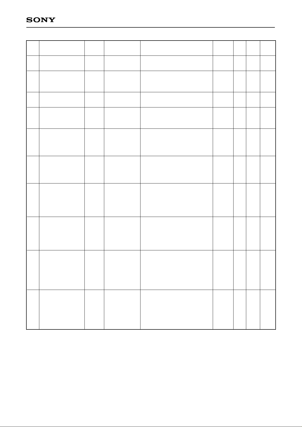
Electrical Characteristics (See Electrical Characteristics Measurement Circuit)
(VDD = 5V, VCC = 15.5V, VSIGCEN = 7V, Ta = 25 ± 3°C)
No. Item Symbol
Measurement contents
Min. Typ.
Max. Unit
1
2
3
4
5
6
7
8
9
10
11
12
VDD current
consumption
VCC current
consumption
Input – output gain
Invert amplifier
gain
Invert amplifier
slew rate
Invert amplifier
output band width
Output delay
deviation for
inverse/noninverse
SID output gain
SID block output
slew rate
VCOM adjustable
range
First stage
SH_OUT
slew rate
SH_OUT
slew rate
IDD
ICC
ASHOUT
AINV
SRINV
BWINV
TDIFF
ASID
SRSID
VCOM
SRSH1
SROUT
IDD = IVDD
ICC = IVCC1 + IVCC2
ASHOUT = VSHOUT (AC)/VIN
AINV = VINV (AC)/VIN
Input a square wave from VIN
so that the VINV output
amplitude is 3.0Vp-p.
Measure the slew rate at 10 to
90% of output waveform rise
or fall. (for inverse or noninverse)
Input 2.5V DC, 100mVp-p AC
from Pin 47 (VIDEO_IN) and
measure VINV. The frequency
that is –3dB to 100kHz. (for
inverse or non-inverse)
Invert amplifier delay time
difference for inverse and noninverse.
ASID = VSID (AC)/VSID_IN
Input an invert pulse to Pin 44
(FRP), load capacitance C7 =
47pF, and apply DC input
voltage to VSID_IN so that VSID
is 2.5V/11.5V.
Measure the slew rate at 10 to
90% of output waveform rise
or fall.
VCOM output voltage when
Pin 34 (VCOMOFF) is varied
from 0 to 10V.
First stage sample-and-hold
slew rate on Block Diagram.
Input a square wave from VIN
so that the VOUT1 to VOUT6
output amplitude is 3.5Vp-p.
Measure the slew rate at 10 to
90% of output waveform rise
or fall. (load 270pF, for inverse
or non-inverse)
20
30
—
—
—
—
—
—
30
Vsig – 2
—
—
28
45
3
2
700
90
2
4
50
—
700
150
42
65
—
—
—
—
4
4.4
—
Vsig
—
—
mA
mA
times
times
V/µs
MHz
ns
times
V/µs
V
V/µs
V/µs
Measurement
points
IVDD
IVCC1
IVCC2
VSHOUT
VIN
VINV
VIN
VINV
VINV
VINV
VSID
VSID_IN
VSID
VCOM
—
VOUT1 to
VOUT6
Page 9
– 9 –
CXA3512R
13
14
15
16
17
18
19
20
21
22
MCLK input
frequency range
TG operating
frequency range
VIDEO_I input
signal range
VIDEO_I input
signal amplitude
range
SHOUT minimum
output voltage
SHOUT maximum
output voltage
Output deviation
between
channels 1
Output deviation
between
channels 2
Output deviation
between ICs 1
Output deviation
between ICs 2
fMCLK
fTG
VINR
VIN
VMIN
VMAX
DOUT1
DOUT2
DIC1
DIC2
D1OR2 = High
(CLKOUT = MCLK)
Maximum frequency at which
the sample-and-hold timing
pulse is output properly.
VIDEO_I input voltage range
when VIDEO_R is set to 3.3V.
Maximum signal amplitude
range of VIDEO_I input signal
Minimum voltage at which
sample-and-hold output
(SHOUT 1 to SHOUT 6) can
be output.
Maximum voltage at which
sample-and-hold output
(SHOUT 1 to SHOUT 6) can
be output.
Value obtained by subtracting
minimum VOUT1 to VOUT6 value
from maximum VOUT1 to VOUT6
value when CAL_R = 2.6V
and VIDEO_I = 2.6V.
Value obtained by subtracting
minimum VOUT1 to VOUT6 value
from maximum VOUT1 to VOUT6
value when CAL_R = 2.6V
and VIDEO_I = 3.3V or 1.9V.
Value obtained by subtracting
minimum VOUT1 to VOUT6 value
from maximum VOUT1 to VOUT6
value when CAL_R = 2.6V
and VIDEO_I = 2.6V.
(when using two CXA3512R)
Value obtained by subtracting
minimum VOUT1 to VOUT6 value
from maximum VOUT1 to VOUT6
value when CAL_R = 2.6V
and VIDEO_I = 3.3V or 1.9V.
(when using two CXA3512R)
14
—
1.5
—
1.5
—
—
—
—
—
—
—
—
—
2
13
4
4
10
10
65
120
3.7
1.5
—
13.5
10
40
20
60
MHz
MHz
V
V
V
V
mVp-p
mVp-p
mVp-p
mVp-p
—
—
—
VOUT1 to
VOUT6
VOUT1 to
VOUT6
VOUT1 to
VOUT6
VOUT1 to
VOUT6
VOUT1 to
VOUT6
VOUT1 to
VOUT6
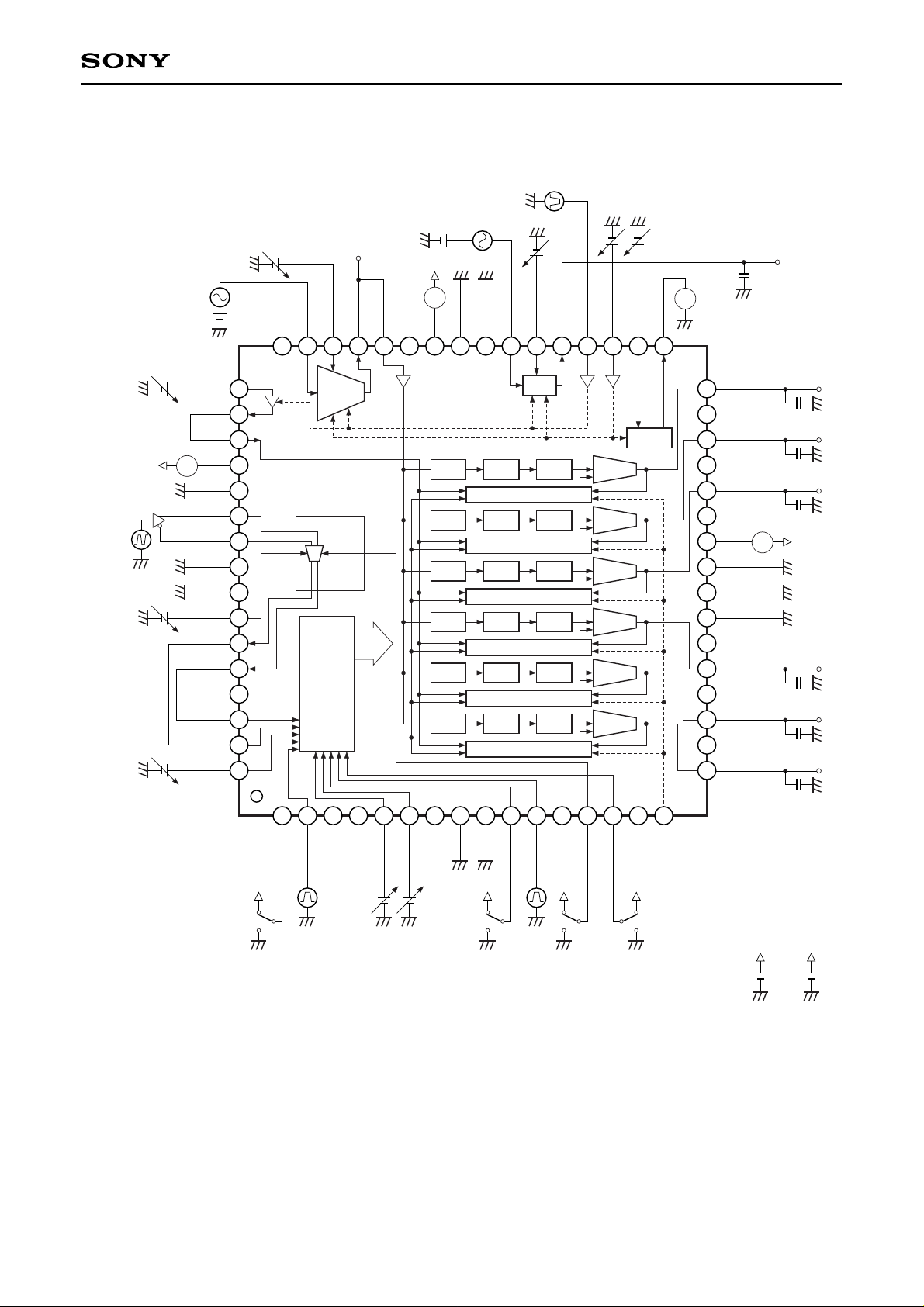
Unless otherwise specified, pin setting conditions are as follows.
(46) VIDEO_R = 3.3V, (47) VIDEO_I = 2.0V, (39) SID_IN = 2.3V, (38) SID_R = 3.3V, (35) SIGCNT = 7.0V,
(34) VCOMOFF = 0V, (1) PRGPOL = 0V, (5) POSCTR1 = 0V, (6) POSCTR2 = 0V, (10) STATUS = 0V,
(13) D1OR2 = 5V, (14) DIRCTR = 5V, (49) CAL_R = 2.6V, (58) DLYCTR = 4.0V, (64) F/H_CNT = 0V,
(36) FRP = 0V, fCLK32.5MHz
No. Item Symbol
Measurement contents
Min. Typ.
Max. Unit
Measurement
points
Page 10
– 10 –
CXA3512R
Electrical Characteristics Measurement Circuit
VDD
SW2
VDD
SW3
VDD
SW4
V
CC VDD
DIFF
BUFFER2
Frequency
f
CLK
2.0V
VIN
S/H S/H S/H
VCOM
OFFSET CANCEL
BUFFER
S/H S/H S/H
OFFSET CANCEL
BUFFER
S/H S/H S/H
OFFSET CANCEL
BUFFER
S/H S/H S/H
OFFSET CANCEL
BUFFER
S/H S/H S/H
OFFSET CANCEL
BUFFER
S/H S/H S/H
OFFSET CANCEL
BUFFER
D
CLOCK
DELAY
S/H
pulses
TIMING
GENERATOR
offset
cancel
mode
timing
SID
INVERT
AMP
CALIBRATION
AMP
1 2 3 4 5 6 7 8 9 10 11 12 13 14 15 16
17
18
19
20
21
22
23
24
25
26
27
28
29
30
31
32
33343536373839404142434445464748
49
50
51
52
53
54
55
56
57
58
59
60
61
62
63
64
CAL_R
CAL_O
CAL_I
V
DD
DGND
MCLK
MCLKX
GND
GND
DLYCTR
CLKOUT
CLKOUTX
NC
CLKIN
CLKINX
PRGPOL
PRG
NC
NC
POSCTR1
POSCTR2
NC
GND
GND
STATUS
ENB
D1OR2
DIRCTR
NC
NC
DCFBSW
NC
VIDEO_I
VIDEO_R
VIDEO_O
SH_IN
NC
V
CC
GND
GND
SID_IN
SID_R
SID_O
FRP
SIGCNT
VCOMOFF
VCOMOUT
SHOUT1
NC
SHOUT2
NC
SHOUT3
NC
PV
CC
GND
GND
PGND
NC
SHOUT4
NC
SHOUT5
NC
SHOUT6
F/H_CNT
V
15.5V
2.3V
VDD
VDD
VCC
IVCC1
VCOM
VSID_IN
VINV
VSID
C1 270pF
V
OUT1
C2 270pF
V
OUT2
C3 270pF
V
OUT3
C4 270pF
V
OUT4
C5 270pF
V
OUT5
C6 270pF
V
OUT6
A
IVDD
A
VCC
IVCC2
A
SW1
5V
Page 11
– 11 –
CXA3512R
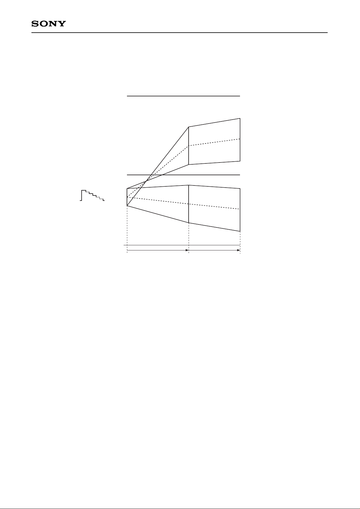
Level Diagram
VIDEO_I to SHOUT
(SIGCNT = 7V, VIDEO_R = input 100% white level)
3.333V
10.667V
V
CC
SIGCNT = 7V
VIDEO_I = 1.5Vp-p
V white
V black
GND
VIDEO_I
2.0 times
VIDEO_O
SH_IN
SHOUT
1.5 times
6.333V
7.667V
12.5V
8V
6V
1.5V
VIDEO_I to VIDEO_O
The formulas for calculating the VIDEO_I to SHOUT internal DC gain are as follows.
For non-inverse:
VIDEO_O = 2.0 × (VIDEO_I – VIDEO_R) + SIGCNT × (1 – 1/10.5)
SHOUT = 3.0 × (VIDEO_I – VIDEO_R) + SIGCNT × (1 – 1/7)
For inverse:
VIDEO_O = –2.0 × (VIDEO_I – VIDEO_R) + SIGCNT × (1 + 1/10.5)
SHOUT = –3.0 × (VIDEO_I – VIDEO_R) + SIGCNT × (1 + 1/7)
Page 12
– 12 –
CXA3512R
Description of Operation
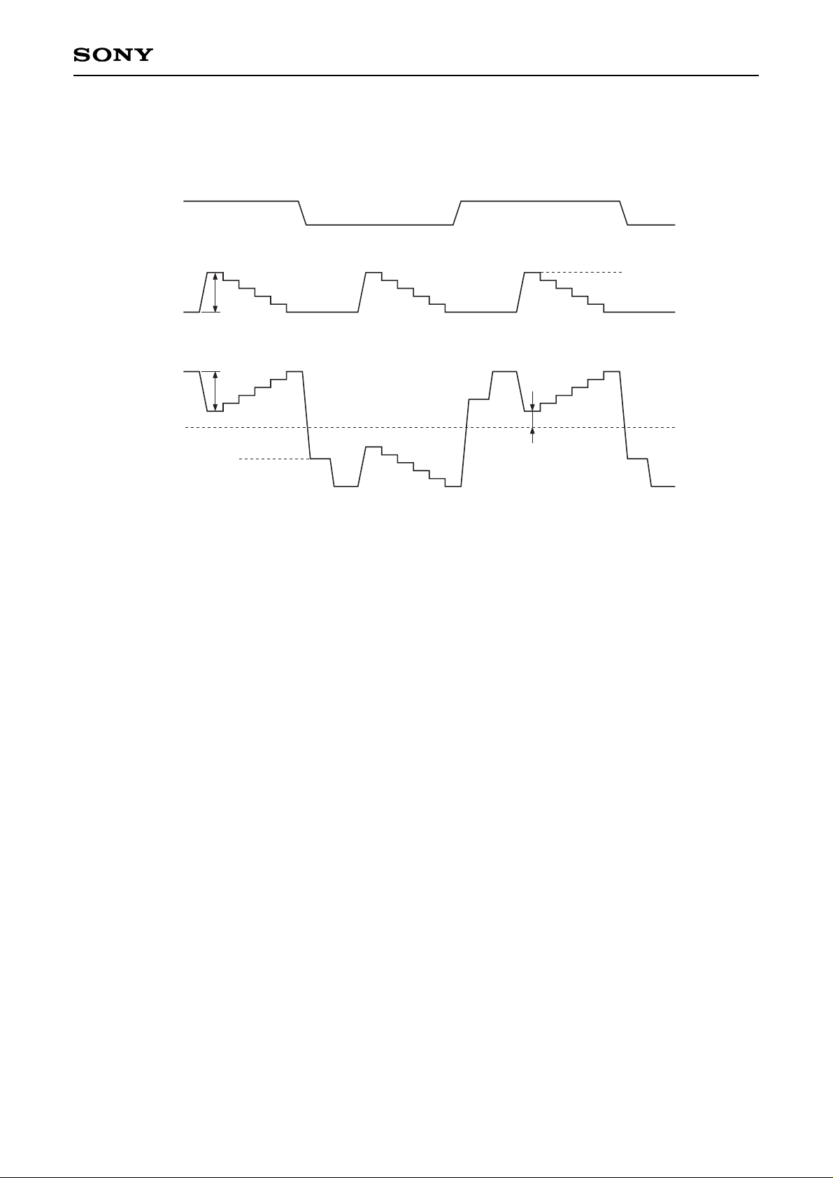
1. Invert Amplifier Block
VIDEO_R
VIDEO_O
VIDEO_I
FRP
V
IN
approx.
3×VIN
approx.
1V
V
SIGCNT
input level
(100% white)
Calibration level
The CXA3512R is designed so that the optimal signal for the LCD panel is output from the SHOUT pins when
a signal in the range from 1.8 to 3.3V is applied to the VIDEO_I input. As shown in the figure above, when a γ
corrected video signal is input to VIDEO_I, the signal is inverse/non-inverse amplified according to the FRP
input (TTL level) and output from VIDEO_O. The DC level is determined by the VIDEO_R input. Input a level
equivalent to 100% white of input. Also, when not using the invert amplifier, connect VIDEO_I to 5V.
2. Analog Demultiplexer Block
The SH_IN analog input signal is converted from a time series signal to a 6-channel (or 12-channel) cyclic
parallel signal by the sample-and-hold group which is appropriately controlled by the on-chip timing generator.
These signals pass through a fixed-gain (= 1.5 times) buffer amplifier and are output to SHOUT. These outputs
can directly drive the input load of the LCD panel.
When using a SVGA panel, connect the (6-channel output) VIDEO_O output directly to the adjacent SH_IN.
XGA panels use 12-channel output, so short the SH_IN of two CXA3512R and connect them to the VIDEO_O
output of one of the IC. The on-chip TG recognizes master/slave by the low/high STATUS (Pin 10) input. For
forward scan, the output alternates between the ICs in the order of master SHOUT1 → slave SHOUT1 →
master SHOUT2 → slave SHOUT2 → master SHOUT3 and so on. Connect the wiring to the LCD panel inputs
in this order.
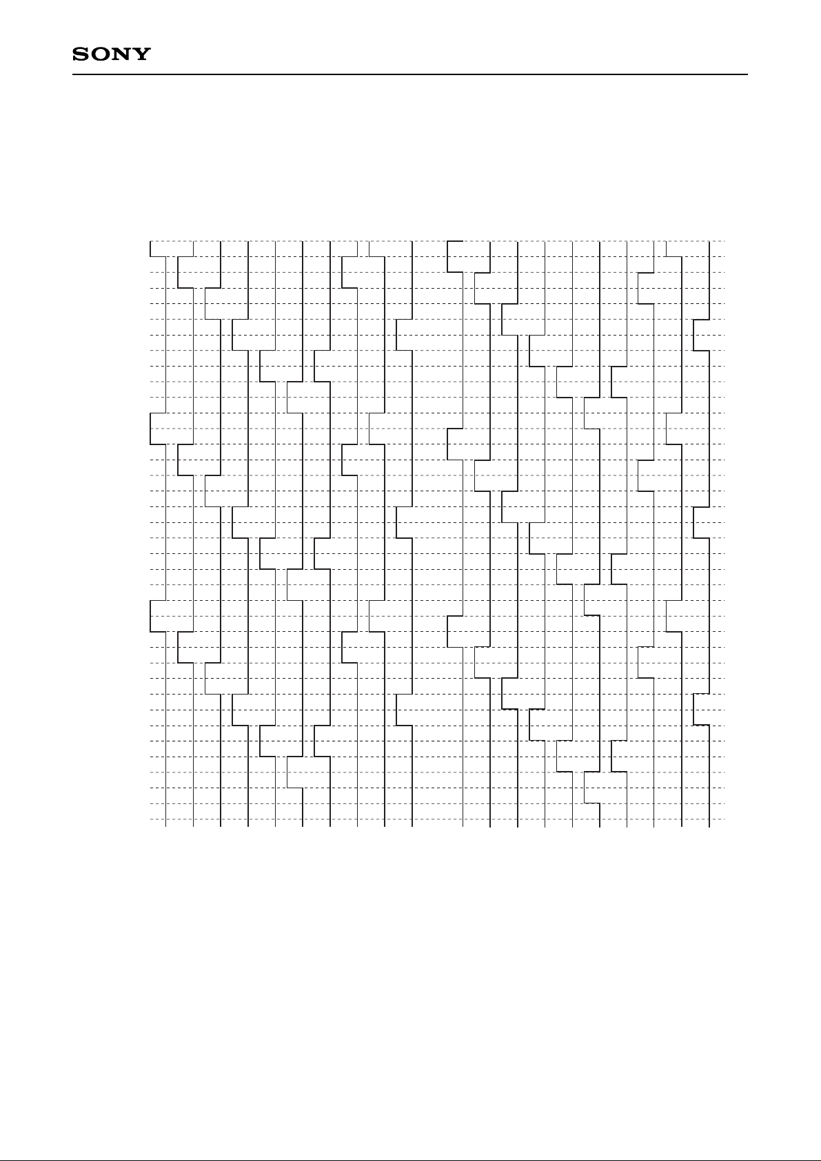
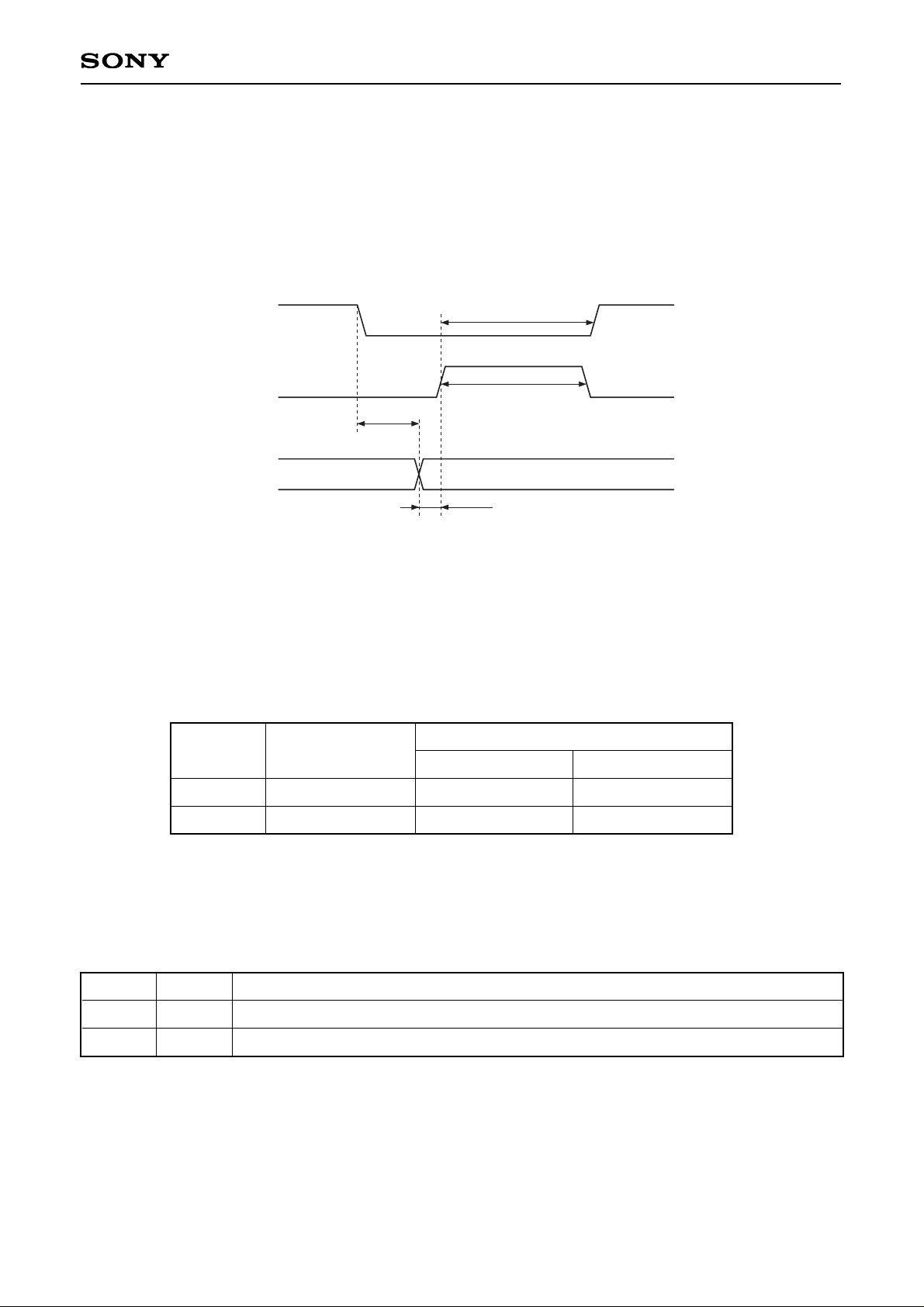
The sample-and-hold pulse generation timing is shown on the following pages. These pulses are not output
and are used only inside the IC.
Page 13

– 13 –
CXA3512R
Internal Sample-and-Hold Pulse Timing Chart 1
Forward scan (DIRCTR = high), F/H_CNT = high
SH1_1ch
SH1_6ch
SH1_2ch
SH1_5ch
SH1_3ch
SH1_4ch
SH1_4ch
SH1_3ch
SH1_5ch
SH1_2ch
SH1_6ch
SH3_4 to 6
SH1_1ch
SH2_1 to 3
SH2_4 to 6
SH2_4 to 6
SH2_1 to 3
SH3_1 to 3
SH3_4 to 6
Slave
(STATUS = high)
Master
(STATUS = low)
When F/H_CNT = low:
same timing as SH3_1 to 3
When F/H_CNT = low:
same timing as SH3_1 to 3
SH3_1 to 3
Page 14
– 14 –
CXA3512R
Internal Sample-and-Hold Pulse Timing Chart 2
Reverse scan (DIRCTR = low), F/H_CNT = high
SH1_1ch
SH1_6ch
SH1_2ch
SH1_5ch
SH1_3ch
SH1_4ch
SH1_4ch
SH1_3ch
SH1_5ch
SH1_2ch
SH1_6ch
SH3_4 to 6
SH1_1ch
SH2_1 to 3
SH2_4 to 6
SH2_4 to 6
SH2_1 to 3
SH3_1 to 3
SH3_4 to 6
Slave
(STATUS = high)
Master
(STATUS = low)
When F/H_CNT = low:
same timing as SH3_4 to 6
When F/H_CNT = low:
same timing as SH3_4 to 6
SH3_1 to 3
Page 15
– 15 –
CXA3512R
3. Timing Generator (TG) Block
The on-chip TG operates by one pair of differential clock inputs (CLK_IN, CLK_INX) and two horizontal sync
signal inputs (PRG, ENB), and generates the timing pulses needed by the demultiplexer block and the output
deviation cancel circuit. The various operation modes can be designated by the pin voltage settings.
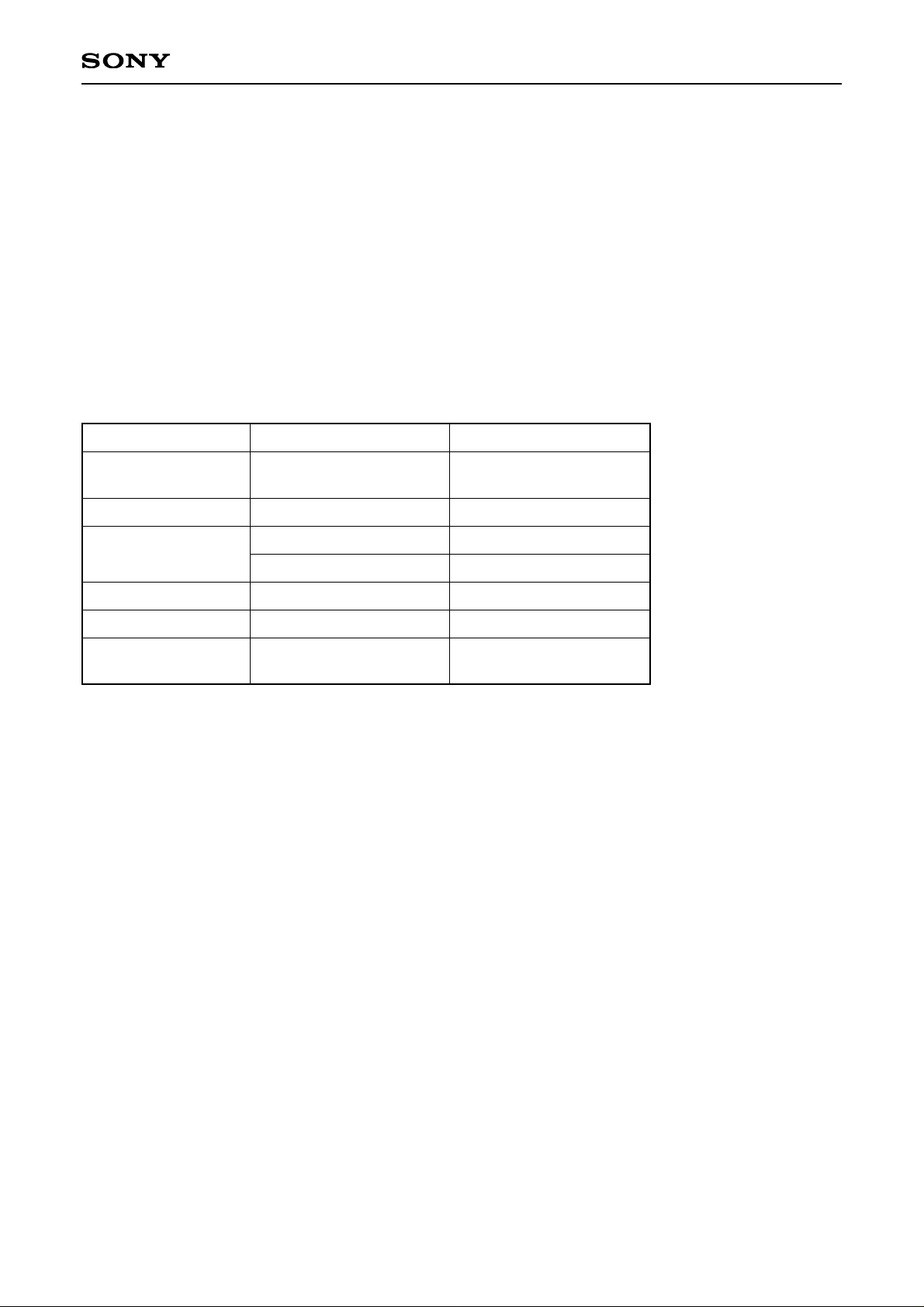
• Input timing signal conditions
30 clk or more
60 clk or more
4 clk or more
ENB
PRG
FRP
0 to 5 clk
Maintain the ENB, PRG and FRP phase relationship shown in the timing chart above, with the CLK_IN input
sync as 1 clk. In particular, when FRP changes between high and low, be sure to input ENB and PRG as
shown above. Otherwise, the IC may suffer irrecoverable deterioration in the worst case.
• Operation mode setting
Table B.
∗1
The output phase can be shifted by 1/2-dot clock in SVGA/SXGA mode by changing STATUS.
STATUS
D1OR2
H/L
∗1
L
SVGA (6-channel mode)
SXGA (12-channel mode)
L
H
XGA/UXGA (12-channel/24-channel mode)
H
H
SlaveMaster
• Scan direction setting
The output scan direction can be changed by the DIRCTR (Pin 14) input.
Pin 14
H
L
Direction
Forward
Reverse
Scan order
SHOUT1 → SHOUT2 → SHOUT3 → SHOUT4 → SHOUT5 → SHOUT6 → SHOUT1 →
SHOUT6 → SHOUT5 → SHOUT4 → SHOUT3 → SHOUT2 → SHOUT1 → SHOUT6 →
The scan direction can be changed by the Pin 14 setting without changing other connections even when using
two CXA3512R such as in XGA mode.
Page 16

– 16 –
CXA3512R
• Output phase setting
The phase of each SHOUT output relative to the analog input can be adjusted in CLK_IN clock units by the
Pins 5 and 6 input levels.
Each input pin has 4 setting values, for a total of 16 settings.
POSCTR1 is the lower bits setting, POSCTR2 is the upper bits setting, and the setting values are as shown in
Table A-1.
Setting value Threshold
0
1
2
3
to 0.75V
1.15 to 1.50V
1.70 to 2.55V
2.95V to
Table A-1. Setting Voltage Range
for Output Phase
Setting value a
0
1
2
3
L
Hi-Z
Hi-Z
H
b
L
L
H
H
Table A-2. CMOS Logic Connection Setting
Value and CMOS Output Pins
There are two ways to use these pins.
A. Connect directly to the CXA2111R
Connect to the corresponding CXA2111R pins POS_CNT1 and POS_CNT2. This allows bit setting via the
CXA2111R I2C bus.
B. Connect to CMOS logic
Connect CMOS logic as shown in the figure. This allows digital control by tri-state control of Pin a. See
Table A-2.
R1 is a threshold setting resistor that provides the voltage for setting values 1 and 2. The appropriate
resistance value changes depending on the number of CXA3512R driven by one CMOS logic (1-channel or 3channel RGB drive, or one CXA3512R (6-outputs/ch) or two CXA3512R (12-outputs/ch)).
Recommended resistance values are given in Table A-3.
CMOS Logic Connection
CXA3512R Usage and Threshold Setting Resistor R1
5b
a
CMOS
CXA3512R
R1
POS_CNT1 or
POS_CNT2
(Pin 6)
Table A-3.
R1 value 250kΩ 150kΩ
RGB 1-channel drive RGB 3-channel drive
100kΩ 47kΩ
12 outputs6 outputs6 outputs 12 outputs
CMOS supply voltage = 3.3 to 5V
Page 17

– 17 –
CXA3512R
4. Dot Clock Phase Adjustment Block
The CXA3512R has a function for adjusting the phase between the analog video input and the dot clock input
to achieve stable reproduction of high definition images. Images with no jitter and flicker can be reproduced by
optimizing the setting.
The 1/2-dot clock input to MCLK and MCLKX (PECL level) is input to the phase comparator of the on-chip PLL
clock generator. The output from CLKOUT and CLKOUTX becomes the internal VCO output. CLKOUT is the
same frequency as MCLK when the D10R2 (Pin 13) input is high, and twice the MCLK frequency when the
D10R2 input is low.
A large amplitude logic with a threshold value of 1.5V can also be connected directly to MCLK instead of
PECL. In this case, connect MCLKX to GND via a capacitor of approximately 100pF. (PECL level input is
recommended when the MCLK input is used around 50MHz.)
The CLKOUT phase can be adjusted up to ±180° according to the DC level (3 to 5V) of the DLYCTR (Pin 58)
input.
By connecting CLKOUT to the TG clock input, the analog video signal and first stage sample-and-hold phases
can be finely adjusted using the DLYCTR DC level.
When using two CXA3512R in XGA mode, input the CLKOUT of one CXA3512R to the CLKIN of both in order
to match the timing of both ICs. In this case, input the same clock to MLCK of both ICs.
5. Calibration Amplifier Block
The CXA3512R generates the deviation cancel circuit reference with a calibration amplifier in order to minimize
the deviation between channels at the highest visibility level.
Input DC level equivalent to approximately 50% gray at VIDEO_I to CAL_R (Pin 49). In addition, directly
connect the CAL_O (Pin 50) output to the adjacent CAL_I.
When using two CXA3512R in XGA mode, connect the CAL_O of one IC to the CAL_I of both ICs, and
connect the unused CAL_R to 5V.
6. SID Block
This block generates the precharge signal used by the LCD panel.
The signal input to SID_IN (Pin 39) is folded at the SIGCNT potential by FRP in the same manner as the invert
amplifier, and output to SID_O (Pin 37). The gain is designed at approximately 4 times. The DC level is
determined by SID_R, and is normally approximately 3.3V.
SID_O cannot directly drive the precharge signal input of the LCD panel. Therefore, connect SID_O via a
buffer having sufficient current supply capability.
SID_O DC calculation formula
Pin 36: low = non-inverse
SID_O = 4 × (SID_IN – SID_R) + 6/7 (SIGCNT)
Pin 36: high = inverse
SID_O = 4 × (SID_R – SID_IN) + 8/7 (SIGCNT)
7. VCOM Block
This block sets the DC potential of the VCOM level.
The VCOMOFF (Pin 34) potential sets the deviation relative to the SIGCNT potential as follows.
VCOMOFF = 0V: VCOMOUT = SIGCNT
VCOMOFF = 10V: VCOMOUT = SIGCNT – 3V
Page 18
– 18 –
CXA3512R
Combination with the CXA2111R
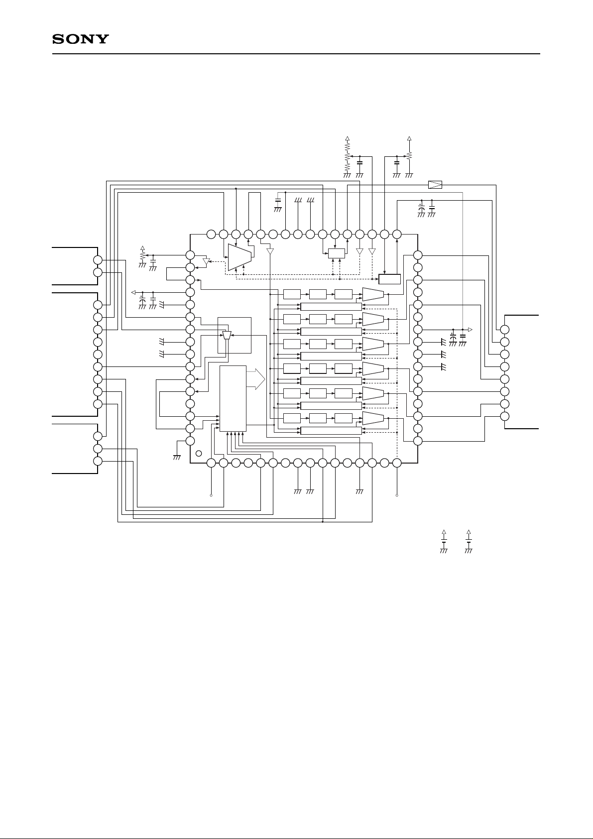
Used together with the CXA2111R, the CXA3512R can achieve most of the analog signal processing (γ
correction, precharge waveform generation) required by LCD panels.
In addition, I2C serial control of the following functions is possible using the I2C-controlled registers built into
the CXA2111R.
• Output phase adjustment (POSCTR1, 2)
• Clock phase adjustment (DLYCTR)
• Scan direction (DIRCTR)
Connect the pins as shown in the table below to use the various functions.
For details, see the CXA2111R specifications.
CXA2111R CXA3512R
ROUT (18), GOUT (16) or
BOUT (14)
SIDOUT (6)
POS_CNT (1)
POS_CNT (2)
DLK_CNT (3)
DIR_CNT (4)
V33 (8)
Video signal
Precharge waveform
Output phase
Clock phase
Scan direction
Reference level
VIDE_IN (47)
SID_IN (39)
POSCTR1 (5)
POSCTR2 (6)
DLYCTR (58)
DIRCTR (14)
VIDEO_R (46)
SID_R (38)
Page 19

– 19 –
CXA3512R
Notes on Operation
1. Notes on Mounting
• The CXA3512R consumes power of approximately 1W. Be sure to take the following measures to prevent
the IC temperature from rising.
A. Pins 8, 9, 24, 25, 40, 41, 56 and 57 (total 8 pins) are connected directly to the "die pad". Electrically
and thermally connect these pins to the inner layer GND plane of a 4-layer substrate using multiple via.
B. Do not mount in high density on a small substrate. Mounting to a 4-layer substrate with an inner layer
copper foil thickness of 30µm or more is recommended.
C. Do not locate the CXA3512R downwind of high thermal loads (lamp, etc.) in sets with fans.
Do not locate the CXA3512R in portions with stagnant air flows in sets without fans.
• The wiring for the CXA3512R alone does not require special consideration, the skew with the PRG pulse
rise timing may cause problems when using a high-speed dot clock. Particularly when using multiple
CXA3512R, the timing of the PRG used as the time reference inside the IC must be matched at the IC
input pins. Care should be taken when designing the board for the effects of propagation time and
reflection, with the PRG line also considered an analog line like MCLK.
If skew with the PRG pulse poses a problem after adjusting the phase relationship between the analog
video input and CLK_IN, it may be possible to solve this problem by adjusting the PRGPOL (Pin 1) H/L
setting for each IC.
2. Input Signals
• Be sure to maintain the FRP, ENB and PRG timings noted in "Description of Operation 3. Timing
Generator (TG) Block".
Special care should be taken to avoid FRP transition without ENB and PRG.
• There is no particular problem when connecting the VIDEO_O output to SH_IN, but in this case do not
input voltages of 2V or less, or (VDD – 2V) or more.
Page 20
– 20 –
CXA3512R
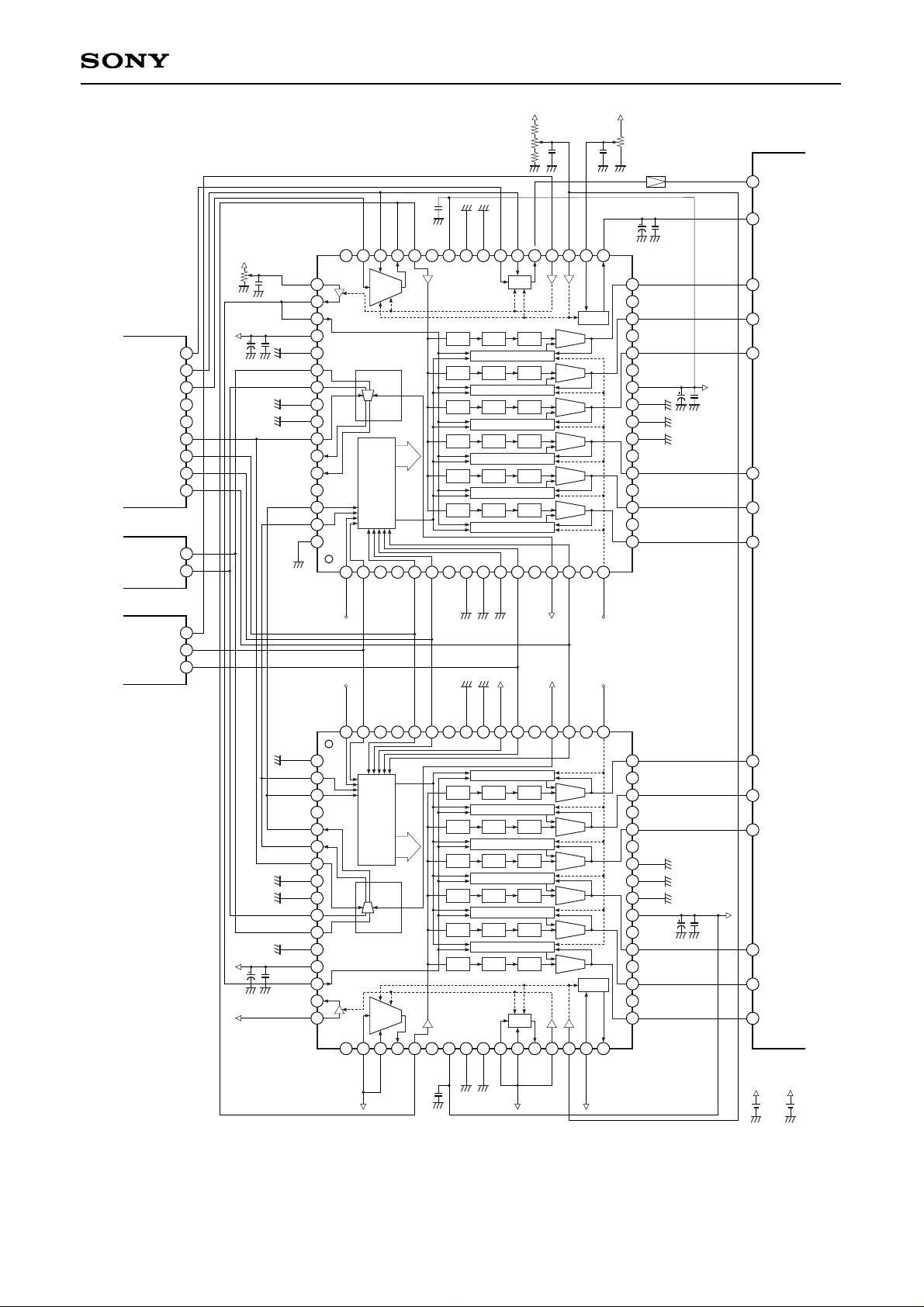
Application Circuit 1 (to SVGA Panel)
VDD VCC
S/H S/H S/H
VCOM
OFFSET CANCEL
BUFFER
S/H S/H S/H
OFFSET CANCEL
BUFFER
S/H S/H S/H
OFFSET CANCEL
BUFFER
S/H S/H S/H
OFFSET CANCEL
BUFFER
S/H S/H S/H
OFFSET CANCEL
BUFFER
S/H S/H S/H
OFFSET CANCEL
BUFFER
D
CLOCK
DELAY
S/H
pulses
TIMING
GENERATOR
offset
cancel
mode
timing
SID
INVERT
AMP
CALIBRATION
AMP
1 2 3 4 5 6 7 8 9 10 11 12 13 14 15 16
17
18
19
20
21
22
23
24
25
26
27
28
29
30
31
32
33343536373839404142434445464748
49
50
51
52
53
54
55
56
57
58
59
60
61
62
63
64
CAL_R
CAL_O
CAL_I
V
DD
DGND
MCLK
MCLKX
GND
GND
DLYCTR
CLKOUT
CLKOUTX
NC
CLKIN
CLKINX
F/H_CNT
PRGPOL
PRG
NC
NC
POSCTR1
POSCTR2
NC
GND
GND
STATUS
ENB
D1OR2
DIRCTR
NC
NC
DCFBSW
NC
VIDEO_I
VIDEO_R
VIDEO_O
SH_IN
NC
V
CC
GND
GND
SID_IN
SID_R
SID_O
FRP
SIGCNT
VCOMOFF
VCOMOUT
SHOUT1
NC
SHOUT2
NC
SHOUT3
NC
PV
CC
GND
GND
PGND
NC
SHOUT4
NC
SHOUT5
NC
SHOUT6
20k
BUFFER
0.1µ
0.1µ
V
CC
10k
5.1k
5.1k
5V
V
CC
20k
V
DD
VDD
0.1µ
0.1µ
VCC
0.1µ
Psig
LCD panel
10µ
15.5V
0.1µ
10µ
1
COM
24
Sig1
7
Sig2
5
Sig3
3
Sig4
2
Sig5
4
Sig6
6
SID_OUT
CXA2111R
6
V33
8
R_OUT
18
CLK H
CXA3106Q
32
CLK L
31
G_OUT
16
FRP
NRG
ENB
B_OUT
14
DLY_CNT
3
POS_CTR1
1
POS_CTR2
2
DIR_CNT
4
OpenOpen
10µ
0.1µ
(LCX026)
Application circuits shown are typical examples illustrating the operation of the devices. Sony cannot assume responsibility for
any problems arising out of the use of these circuits or for any infringement of third party patent and other right due to same.
Page 21
– 21 –
CXA3512R
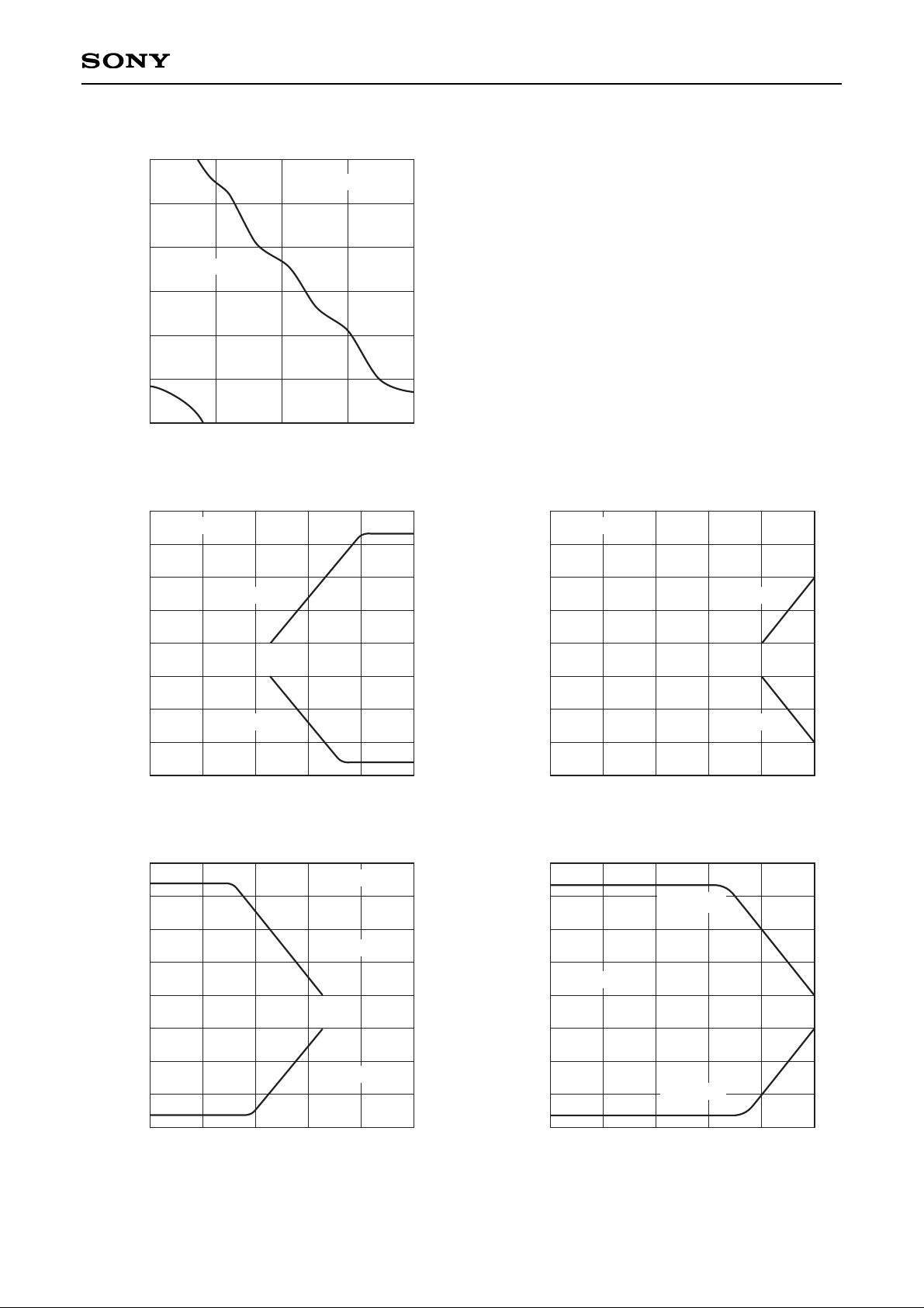
Application Circuit 2 (to XGA Panel)
S/H S/H S/H
VCOM
OFFSET CANCEL
BUFFER
S/H S/H S/H
OFFSET CANCEL
BUFFER
S/H S/H S/H
OFFSET CANCEL
BUFFER
S/H S/H S/H
OFFSET CANCEL
BUFFER
S/H S/H S/H
OFFSET CANCEL
BUFFER
S/H S/H S/H
OFFSET CANCEL
BUFFER
D
CLOCK
DELAY
S/H
pulses
TIMING
GENERATOR
offset
cancel
mode
timing
SID
INVERT
AMP
CALIBRATION
AMP
1 2 3 4 5 6 7 8 9 10 11 12 13 14 15 16
17
18
19
20
21
22
23
24
25
26
27
28
29
30
31
32
33343536373839404142434445464748
49
50
51
52
53
54
55
56
57
58
59
60
61
62
63
64
CAL_R
CAL_O
CAL_I
V
DD
DGND
MCLK
MCLKX
GND
GND
DLYCTR
CLKOUT
CLKOUTX
NC
CLKIN
CLKINX
F/H_CNT
PRGPOL
PRG
NC
NC
POSCTR1
POSCTR2
NC
GND
GND
STATUS
ENB
D1OR2
DIRCTR
NC
NC
DCFBSW
NC
VIDEO_I
VIDEO_R
VIDEO_O
SH_INNCV
CC
GND
GND
SID_IN
SID_R
SID_O
FRP
SIGCNT
VCOMOFF
VCOMOUT
SHOUT1
NC
SHOUT2
NC
SHOUT3
NC
PV
CC
GND
GND
PGND
NC
SHOUT4
NC
SHOUT5
NC
SHOUT6
20k
BUFFER
0.1µ
0.1µ
V
CC
VDD VDD
10k
5.1k
5.1k
V
CC
20k
V
DD
VDD
0.1µ
0.1µ
VCC
0.1µ
Psig
LCD panel
(LCX023)
10µ
0.1µ
10µ
1
COM
31
Sig1
3
Sig3
5
Sig5
7
Sig7
9
Sig9
11
Sig11
13
SID_OUT
CXA2111R
6
V33
8
R_OUT
18
CLK H
CXA3106Q
32
CLK L
31
G_OUT
16
B_OUT
14
DLY_CNT
3
POS_CTR1
1
POS_CTR2
2
DIR_CNT
4
OpenOpen
Open Open
S/H S/H S/H
VCOM
OFFSET CANCEL
BUFFER
D
CLOCK
DELAY
S/H
pulses
TIMING
GENERATOR
offset
cancel
mode
timing
SID
INVERT
AMP
CALIBRATION
AMP
1 2 3 4 5 6 7 8 9 10 11 12 13 14 15 16
32
31
30
29
28
27
26
25
24
23
22
21
20
19
18
1764
63
62
61
60
59
58
57
56
55
54
53
52
51
50
49
CAL_R
CAL_O
CAL_I
V
DD
DGND
MCLK
MCLKX
GND
GND
DLYCTR
CLKOUT
CLKOUTX
NC
CLKIN
CLKINX
F/H_CNT
PRGPOL
NRGNCNC
POSCTR1
POSCTR2
NC
GND
GND
STATUS
ENB
D1OR2
DIRCTR
NCNCDCFBSW
NC
VIDEO_I
VIDEO_R
VIDEO_O
SH_IN
NC
V
CC
GND
GND
SID_IN
SID_R
SID_O
FRP
SIGCNT
VCOMOFF
VCOMOUT
SHOUT1
NC
SHOUT2
NC
SHOUT3
NC
PV
CC
GND
GND
PGND
NC
SHOUT4
NC
SHOUT5
NC
SHOUT6
VDD
VDD
VCC
VDDVDDVDD
0.1µ
0.1µ
10µ
V
DD VCC
5V 15.5V
0.1µ
10µ
Sig12
14
Sig10
12
Sig8
10
Sig6
8
Sig4
6
Sig2
4
S/H S/H S/H
OFFSET CANCEL
BUFFER
S/H S/H S/H
OFFSET CANCEL
BUFFER
S/H S/H S/H
OFFSET CANCEL
BUFFER
S/H S/H S/H
OFFSET CANCEL
BUFFER
S/H S/H S/H
OFFSET CANCEL
BUFFER
33343536373839404142434445464748
FRP
NRG
ENB
VDD
0.1µ10µ
Application circuits shown are typical examples illustrating the operation of the devices. Sony cannot assume responsibility for
any problems arising out of the use of these circuits or for any infringement of third party patent and other right due to same.
Page 22
– 22 –
CXA3512R
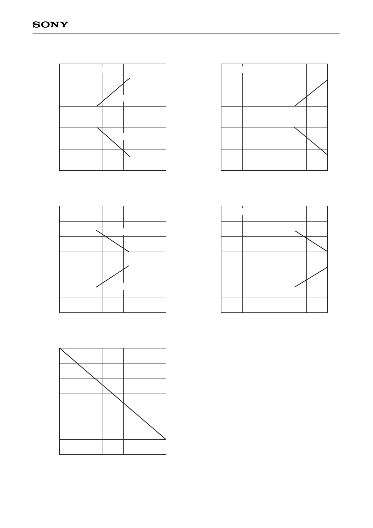
Example of Representative Characteristics (VCC = 15.5V, VDD = 5.0V, SIGCNT = 7.0V, Ta = 25 ± 3°C)
CLKOUT phase to MCLK vs. DLYCTR voltage
DLYCTR (Pin 58) voltage [V]
Phase [deg]
4 4.53
–180
–120
–60
0
60
120
180
3.5 5
SID_O voltage vs. SID_R voltage (1)
SID_R (Pin 38) voltage [V]
SID_O (Pin 37) voltage [V]
3 40
0
2
4
6
8
12
16
10
14
21 5
FRP = High
FRP = Low
SID_IN = 2.3V
SID_O voltage vs. SID_R voltage (2)
SID_R (Pin 38) voltage [V]
SID_O (Pin 37) voltage [V]
3 40
0
2
4
6
8
12
16
10
14
21 5
FRP = High
FRP = Low
SID_IN = 4.0V
SID_O voltage vs. SID_IN voltage (1)
SID_IN (Pin 39) voltage [V]
SID_O (Pin 37) voltage [V]
3 40
0
2
4
6
8
12
16
10
14
21 5
FRP = High
FRP = Low
SID_R = 3.3V
SID_O voltage vs. SID_IN voltage (2)
SID_IN (Pin 39) voltage [V]
SID_O (Pin 37) voltage [V]
3 40
0
2
4
6
8
12
16
10
14
21 5
FRP = High
FRP = Low
SID_R = 5.0V
D1OR2 = HIgh
MCLK = 20MHz
Page 23
– 23 –
CXA3512R
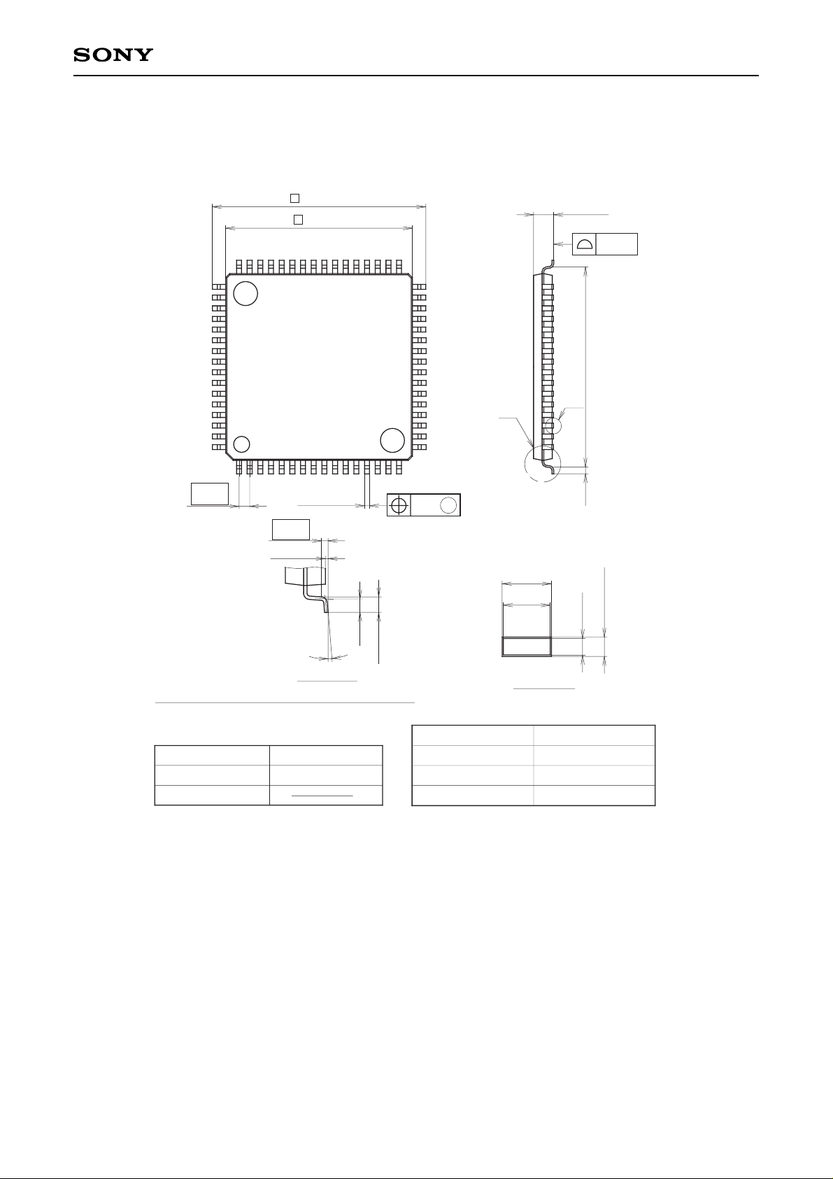
VIDEO_O voltage vs. VIDEO_IN voltage (1)
VIDEO_IN (Pin 47) voltage [V]
VIDEO_O (Pin 45) voltage [V]
3 40
0
2
4
6
8
12
14
10
21 5
FRP = High
FRP = Low
VIDEO_R = 3.3V
VIDEO_O voltage vs. VIDEO_R voltage (1)
VIDEO_R (Pin 46) voltage [V]
VIDEO_O (Pin 45) voltage [V]
2 3 40
2
4
6
8
10
12
1 5
FRP = High
FRP = Low
VIDEO_IN = 1.8V
5
VIDEO_O voltage vs. VIDEO_R voltage (2)
VIDEO_R (Pin 46) voltage [V]
VIDEO_O (Pin 45) voltage [V]
2 3 40
2
4
6
8
10
12
1
FRP = High
FRP = Low
VIDEO_IN = 3.5V
VIDEO_O voltage vs. VIDEO_IN voltage (2)
VIDEO_IN (Pin 47) voltage [V]
VIDEO_O (Pin 45) voltage [V]
3 40
0
2
4
6
8
12
14
10
21 5
FRP = High
FRP = Low
VIDEO_R = 5.0V
VCOMOUT voltage vs. VCOMOFF voltage
VCOMOFF (Pin 34) voltage [V]
VCOMOUT (Pin 33) voltage [V]
6 80
3.5
4.0
4.5
5.0
5.5
6.5
7.0
6.0
42 10
Page 24
– 24 –
CXA3512R
Package Outline Unit: mm
SONY CODE
EIAJ CODE
JEDEC CODE
PACKAGE MATERIAL
LEAD TREATMENT
LEAD MATERIAL
PACKAGE MASS
EPOXY RESIN
PALLADIUM PLATING
COPPER ALLOY
PACKAGE STRUCTURE
LQFP-64P-L02
LQFP064-P-1414
0.7g
0.37 – 0.07
+ 0.08
(0.35)
(0.125)
0.145 ± 0.04
64PIN LQFP (PLASTIC)
0.8
∗ 14.0 ± 0.1
16.0 ± 0.2
48
33
49 32
17
16
1
64
0.37 – 0.07
+ 0.08
A
B
(0.5)
(15.0)
1.7MAX
0.1
0.13
M
0.1 ± 0.1
0.25
(0.5)
0.6 ± 0.2
0° to 10°
DETAIL A
DETAIL B
NOTE: Dimension “∗” does not include mold protrusion.
NOTE : PALLADIUM PLATING
This product uses S-PdPPF (Sony Spec.-Palladium Pre-Plated Lead Frame).
 Loading...