

Page 1

CXA3329ER
Analog Signal Processor TX-IF IC for W-CDMA Cellular Phones
Description
The CXA3329ER is an analog signal processor
TX-IF IC for the W-CDMA cellular phones. This IC
contains voltage-controlled gain control amplifier and
quadrature modulator .
Features
• Gain control amplifier with a linear and wide gain
variable range
• I-Q quadrature modulator
• Power saving switch
• Low voltage operation (2.7 to 3.3V)
• Small package (24-pin VQFN)
Applications
Analog signal processor TX-IF IC for the W-CDMA
cellular phones
24 pin VQFN (Plastic)
Preliminary
Structure
Bipolar silicon monolithic IC
Absolute Maximum Ratings
• Supply voltage Vcc –0.3 to +5.5 V
• Operating temperature Topr –55 to +125 °C
• Storage temperature Tstg –65 to +150 °C
Recommended Operating Conditions
• Supply voltage Vcc 2.7 to 3.3 V
• Operating temperature Ta –25 to +85 °C
Sony reserves the right to change products and specifications without prior notice. This information does not convey any license by
any implication or otherwise under any patents or other right. Application circuits shown, if any, are typical examples illustrating the
operation of the devices. Sony cannot assume responsibility for any problems arising out of the use of these circuits.
– 1 –
PE00Y17-PS
Page 2

Block Diagram
CXA3329ER
CC
PS
VCONT
AGCV
CC2
AGCGND2
OUTX
OUT
19
20
21
22
23
24
NC
GCA control
NC
MODV
MODGND
15 14161718 13
Switch
PVCC
1/4
1/2
PGND
12
11
10
9
8
7
NC
GND4
Local IN
NC
NC
Local SW
4 5321 6
I
AGCVCC1
AGCGND1
IX
Q
QX
– 2 –
Page 3

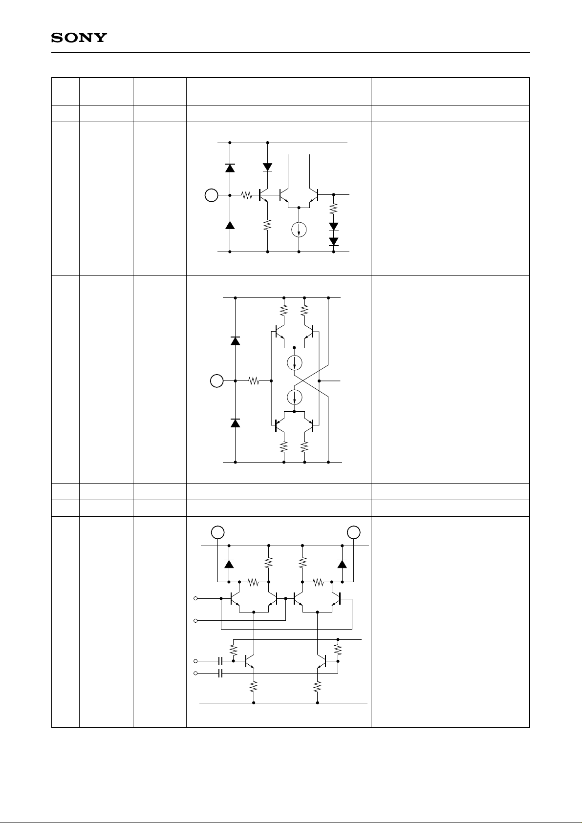
Pin Description
CXA3329ER
Pin
No.
Symbol Equivalent circuit Description
Typical pin
voltage [V]
1 AGCVCC12.85
2 AGCGND1 0
3, 4
5, 6
I, IX
Q, QX
1.425
7 Local SW —
Positive power supply.
Ground.
MODVCC
53
64
30k
7
150
150
2k
MODGND
PV
I, Q inputs.
Applies a bias voltage from the
external source.
CC
Frequency division value selection.
High: 1/4 frequency division
Low: 1/2 frequency division
Open: Low
PGND
8, 9 NC — No connection.
PV
CC
10
10 Local IN — Local input.
50
11
12
13
14
15
16
GND4
NC
PGND
PVCC
MODGND
MODVCC
0
—
0
2.85
0
2.85
0.5k
PGNDGND4
2k
2k
Ground.
No connection.
Ground.
Positive power supply.
Ground.
Positive power supply.
– 3 –
Page 4
CXA3329ER
Pin
No.
17, 18
19 PS
Symbol Equivalent circuit
Typical pin
voltage [V]
NC
40k
60k
8k 8k
—
19
Description
No connection.—
AGCVCC2
Power saving mode switch input.
High: Active mode
Low: Power saving mode
AGCGND2
AGCVCC2
21 AGCV
22
AGCGND2
2324OUTX
OUT
CC2
2.85
—
20
23 24
20k
6k 6k
AGCGND2
AGCVCC1
25 25
890 890
Gain control voltage input.20 VCONT —
Positive power supply.
Ground.0
IF signal differential output.
AGCGND1
– 4 –
Page 5

Input Conditions for Each Pin
CXA3329ER
Pin
No.
3, 4,
5, 6
3, 4,
5, 6
3, 4,
5, 6
7
7
10
10
19
19
20
Item Symbol
I/Q bias voltage
I/Q input voltage
I/Q band width
Local switch voltage-High
Local switch voltage-Low
Local frequency
Local input level
PS voltage-High
PS voltage-Low
Control voltage range
VBIQ
VIQ
BWIQ
VLSH
VLSL
fLO
LO
VPSH
VPSL
VCN
Conditions
Differential input
Min.
1.35
—
—
2.5
0
—
–18
2.0
0
0
Typ.
1.425
0.4
—
760
–15
Max.
1.65
1
5
VCC
0.8
—
–12
VCC
0.8
VCC
Unit
V
Vp-p
MHz
V
V
MHz
dBm
V
V
V
– 5 –
Page 6
Electrical Characteristics
CXA3329ER
Item Symbol
DC Characteristics
Current consumption 1
Current consumption 2
Power saving current
AC Characteristics
Output IP3
Output power 1
Output power 2
Gain control range
Output noise power 1
I, Q residual sideband
product
Carrier leak
Imax
Imin
Ips
OIP3
PO1
PO2
Gcr
No1
Img
CL
Conditions
VCONT = 2.85V
VCONT = 0V
PS = low (in power saving mode)
Note1
VCONT = 2.3V,
differential output, f = 380MHz
VCONT = 0.3V,
differential output, f = 380MHz
VCONT = 0.3 to 2.3V,
f = 380MHz
VCONT = 1.8V,
I/Q inputs are no signal.
Suppression ratio of desired signal
(f = 380 + 1) MHz and image
signal (f = 380 – 1) MHz
Ratio of desired signal
(f = 380 + 1) MHz and local leak
(f = 380) MHz
Measurement
point
A
A
A
B
B
B
B
B
B
B
Min.
—
8.5
–19
–83
54
—
—
—
Typ.
24
17
—
–15
–77
62
—
—
—
Max.
5
–11
–73
70
–147
–25
–18
Unit
mA
µA
dBm
dBm
dB
dBm/
Hz
dBc
Input signal I/Q phase difference
Input I/Q phase error
IQPE
–90° when the output signal I/Q
–3
0
3
B
deg
phase difference is 90°.
I/Q input signal level difference
Input I/Q gain error
IQGE
when the output signal I/Q levels
B
–2.5
0
2.5
dB
are the same.
• Unless otherwise specified, the I/Q baseband input signals and local input signal use the conditions shown in
the Electrical Characteristics Measurement Circuit and the control voltage and power saving pins are set to
VCONT = 2.3V, PS = high.
The local switching pin is left open (1/2 frequency division).
• IF output impedance is 1kΩ.
• Values measured with a Sony evaluation board.
Note1) Set the control voltage so that the output power becomes –15dBm under the conditions shown in
the Electrical Characteristics Measurement Circuit. Input the two tone signals of 570kHz, 200mVp-p
and 630kHz, 200mVp-p to I-IX; and also input to Q-QX the two tone signals whose phases are
deviated by 90 degrees from those signals.
The ratio of the desired component and the 3rd order harmonic component of the outputs resulted
from the above is measured, and the power level that is made by adding the half ratio to the desired
component power level is labeled as the output IP3. See the figure on the next page.
– 6 –
Page 7

Output level
f0 + 510kHz
f0 + 570kHz
f0 + 630kHz
f0 + 690kHz
CXA3329ER
S
OIP3 = S + (S – IM3)/2
A
IM3
Frequency
– 7 –
Page 8
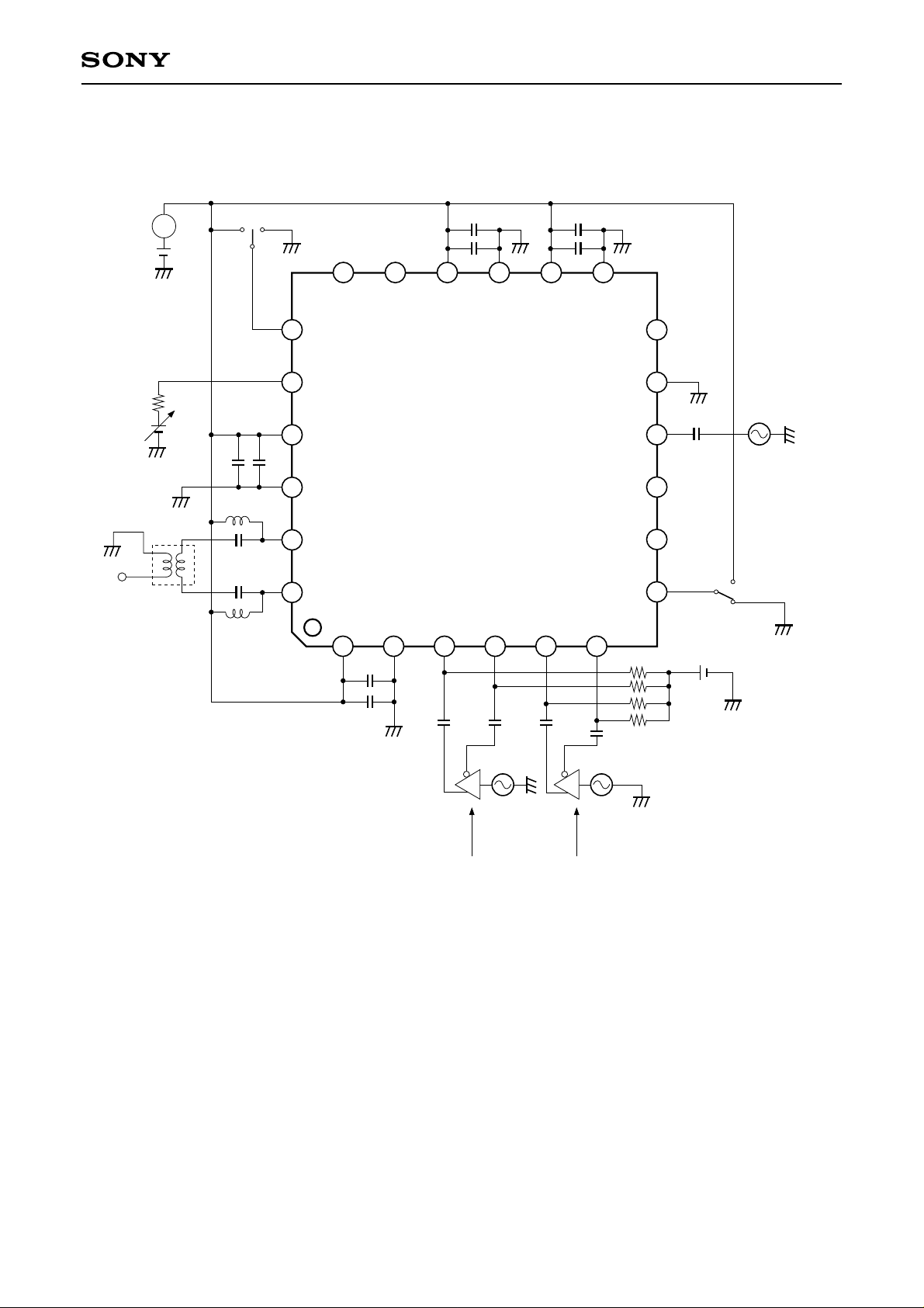
Electrical Characteristics Measurement Circuit
CXA3329ER
Vcc
OUTPUT B
1k
1µ
1µ
A
Active
Power save
19
20
21
1n
1µ
22
∗
1
22n
2
∗
23
NC
PS
VCONT
CC2
AGCV
AGCGND2
OUTX
NC
1n
15 14161718 13
CC
MODV
MODGND
1n
1n
24
OUT
∗
22n
1
AGCVCC1
AGCGND1
I
IX
4 5321 6
1µ
1n
1µ 1µ 1µ
PVCC
Q
1n
Local IN
Local SW
1µ
PGND
GND4
QX
NC
NC
NC
10k
10k
12
11
10
9
8
7
1n
fLO = 760MHz
–15dBm
Local signal input
1/4 frequency
division
1/2 frequency
division
1/2 × Vcc
10k
10k
cos (2πf)
f = 1MHz
400mVp-p
Gain = 1 Gain = 1
Baseband signal input
∗
1
Murata, Inc. LQN21A22NJ (K) 04
∗
2
TOKO, Inc. B5FL 616DS-1135
– 8 –
sin (2πf)
f = 1MHz
400mVp-p
Page 9

Application Circuit
Vcc
CXA3329ER
1k
1n
Active
∗
1n
1n
∗
Power save
PS
19
VCONT
20
AGCV
21
1µ
22
AGCGND2
23
OUTX
∗
24
OUT
NC
CC
2
1
CC
AGCV
1µ
1n
1µ
1n
15 14161718 13
NC
AGCGND1
CC
MODV
I
MODGND
IX
4 5321 6
1µ 1µ 1µ 1µ
CC
PV
Q
1µ
1n
Local IN
Local SW
PGND
GND4
QX
NC
NC
NC
10k
10k
12
11
10
9
8
7
1n
Local signal
1/4 frequency
division
1/2 frequency
division
1/2 × Vcc
10k
10k
Baseband signal
∗
Adjust these values so that the impedance matching with this IC is optimum.
Application circuits shown are typical examples illustrating the operation of the devices. Sony cannot assume responsibility for
any problems arising out of the use of these circuits or for any infringement of third party patent and other right due to same.
– 9 –
Page 10
CXA3329ER
Description of Operation
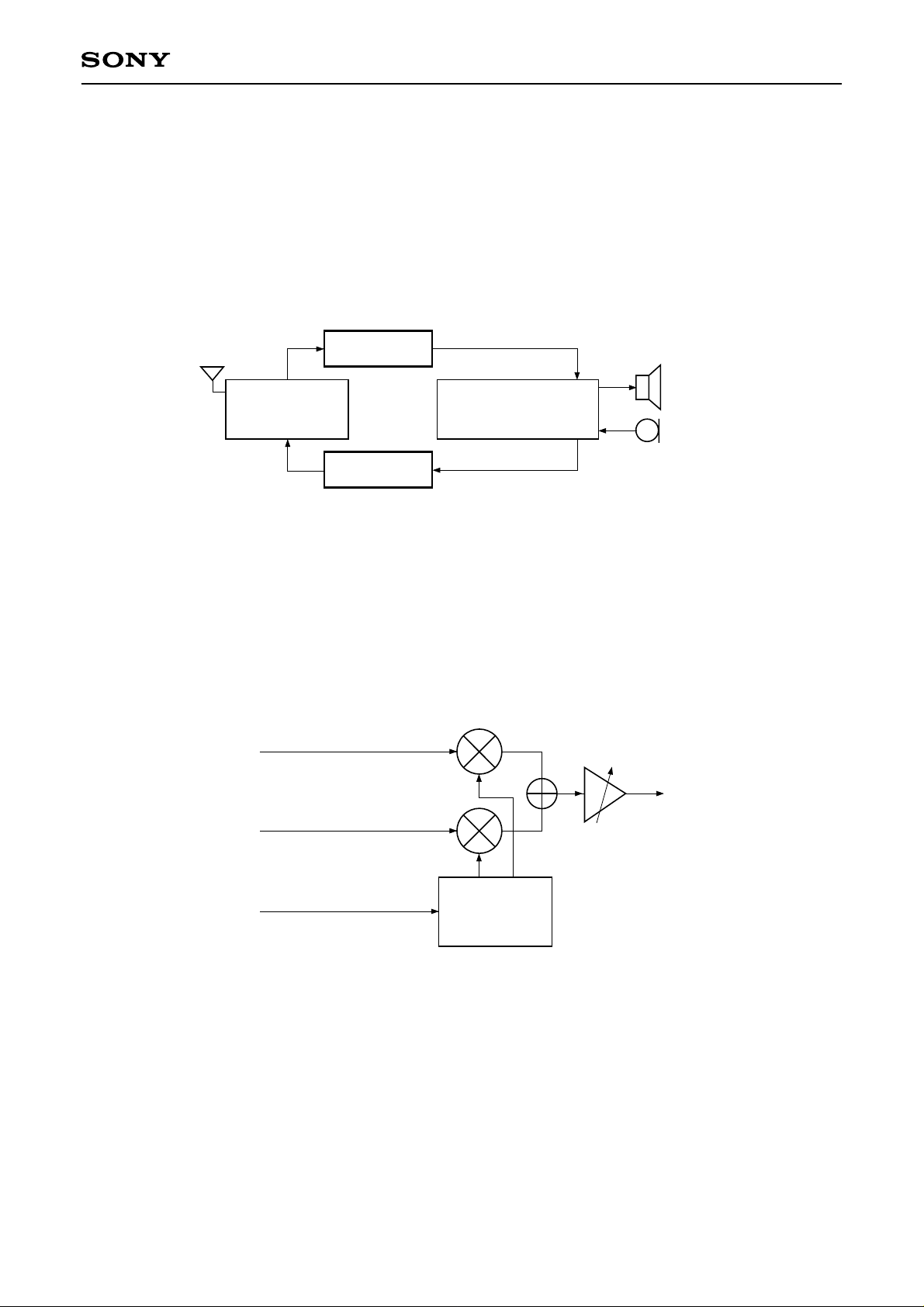
1. Outline of operation
This IC performs the signal processing between the analog transmit baseband processor block and the analog
transmit RF processor block of the cellular phone. The figure below shows the general circuit block diagram for
the portable cellular phones using this IC. The input for this IC is connected to the baseband signal processor
block; the output is connected to the analog RF processor block.
CXA3328TN
RF receive/
transmit processor
CXA3329ER
Baseband signal
processor
2. IC Internal Signal Flow
Two baseband-processed signals I, Q and the local signal are input to this IC as shown in the figure below.
The local signal is 1/2-frequency divided, and that signal becomes the quadrature I/Q local signal. The
baseband I/Q signals are input to the quadrature modulatar, and baseband processing to IF upconversion is
performed with the quadrature local signals. The signal is input to the gain control amplifier, and output after
the gain controlled to the necessary level.
I/IX
OUT/OUTX
Q/QX
Local
–90˚
– 10 –
0˚
1/2 div
(1/4 div)
Page 11

CXA3329ER
Notes on Operation
1. Baseband signal I/Q input
Pins 3 to 6, where the baseband signal is input, do not have a determined voltage internally on the IC.
Therefore, a bias voltage equivalent to 1/2VCC should be applied externally.
2. IF signal output
The IF signal outputs, OUT/OUTX, are differential outputs. The output impedance should be 1kΩ including the
external resistance with differential. Also, it is necessary to connect the inductor to eliminate the parasitic
capacitance in the IC.
3. Notes on power supplies
The CXA3329ER is designed to operate by a 2.85V stabilized power supply to allow use with the battery
driven portable phones. Using the multiple voltage regulators throughout the phone is recommended to
minimize the power supply noise in the CXA3329ER pow er supply unit. The recommended pow er supply r ange
for the CXA3329ER is from 2.7V to 3.3V. Decouple the power supplies around the CXA3329ER using 1µF
capacitor for each VCC pin. Locate this capacitor as close to the pins as possible to minimize the series
inductance. Using an additional 1nF decoupling capacitor in parallel to the 1µF capacitor is recommended to
further reduce the high frequency noise in the power supply input to the CXA3329ER.
– 11 –
Page 12
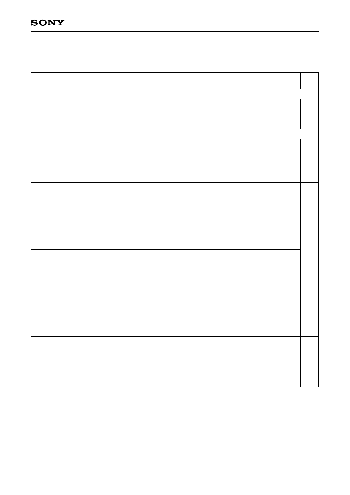
CXA3329ER
Design Materials (Design Guarantee)
Electrical Characteristics (VCC = 2.7 to 3.8V, Ta = –25 to +85°C)
Item Symbol Conditions Min. Typ. Max. Unit
DC Characteristics
Current consumption 1
Current consumption 2
Power saving current
AC Characteristics
Output IP3
Output power 1
Output power 2
Gain control range
Gain accuracy
Gain flatness
Output noise power 1
Output noise power 2
Imax
Imin
Ips
OIP3
PO1
PO2
Gcr
Gct
Gflat
No1
No2
VCONT = 2.85V
VCONT = 0V
PS = low (in power saving mode)
Note1 (See page 6.)
VCONT = 2.3V,
differential output, f = 380MHz
VCONT = 0.3V,
differential output, f = 380MHz
VCONT = 0.3 to 2.3V,
f = 380MHz
Difference between the output
powers where Ta = –25°C, 85°C
and Ta = 27°C
IF ± 2.5MHz
PO = –25dB,
I/Q inputs are no signal.
PO = –65dBm,
I/Q inputs are no signal.
Measurement
point
A
A
A
B
B
B
B
B
B
B
B
—
8.5
–19
–83
54
–2
–0.25
—
—
24
17
—
—
–15
–77
62
0
0
—
—
5
—
–11
–73
70
2
0.25
–147
–162
mA
µA
dBm
dBm
dB
dB
dB
dBm/
Hz
I, Q residual sideband
product
Img
Suppression ratio of desired signal
(f = 380 + 1) MHz and image
signal (f = 380 – 1) MHz
—
—
B
–25
dBc
Ratio of desired signal
Carrier leak
CL
(f = 380 + 1) MHz and local leak
—
—
B
–18
(f = 380) MHz
Input signal I/Q phase difference
Input I/Q phase error
IQPE
–90° when the output signal I/Q
–3
0
3
B
deg
phase difference is 90°.
I/Q input signal level difference
Input I/Q gain error
IQGE
when output signal I/Q levels are
B
–2.5
0
2.5
dB
the same.
Error vector magnitude
Response time
EVM
Tr
Until output rise of 90% after the
power is turned ON.
—
—
3
B
—
—
B
10
%
µs
• Unless otherwise specified, the I/Q baseband input signals and local input signal use the conditions shown in
the Electrical Characteristics Measurement Circuit and the control voltage and power saving pins are set to
VCONT = 2.3V, PS = high.
The local switching pin is left open (1/2 frequency division).
• IF output impedance is 1kΩ.
• Values measured with a Sony evaluation board.
– 12 –
Page 13

Design Materials (Design Guarantee)
CXA3329ER
Item Symbol Conditions Min. Typ. Max. Unit
Input Impedance
I/Q input resistance
I/Q input capacitance
VCONT pin input
resistance
Local IN input
resistance
RIQ
CIQ
RVC
RL
Single
Single
Measurement
point
3, 4, 5, 6
3, 4, 5, 6
20
10
60
—
10
37.5
85
—
—
50
—
10
—
62.5
kΩ
pF
kΩ
Ω
– 13 –
Page 14

Package Outline Unit: mm
CXA3329ER
24PIN VQFN(PLASTIC)
0.1
0.7
S
S
0.9 ± 0.1
A-B
A-B
C
C
0.05
S
Solder Plating
C 0.6
∗1)
0.03 ± 0.03 (
(Stand Off)
TERMINAL SECTION
S
1.0
0.13 ± 0.025
4.0
3.6
C
1318
19
A
PIN 1 INDEX
24
1
0.05
0.4
12
B
7
6
x 4
0.1
x 4
A-B
S
M
C
0.14
4.78
45˚
0.2 ± 0.01
+ 0.09
– 0.03
0.6 ± 0.1
(0.39)
(0.15)
0.225 ± 0.03
SONY CODE
EIAJ CODE
JEDEC CODE
VQFN-24P-03
PACKAGE STRUCTURE
PACKAGE MATERIAL
LEAD TREA TMENT
LEAD MATERIAL
PACKAGE MASS
– 14 –
EPOXY RESIN
SOLDER PLATING
COPPER ALLOY
0.04g
Sony Corporation
 Loading...