

Page 1

CXA3276Q
8-bit 160MSPS Flash A/D Converter
Description
The CXA3276Q is an 8-bit high-speed flash A/D
converter capable of digitizing analog signals at the
maximum rate of 160MSPS. ECL, PECL or TTL can
be selected as the digital input level in accordance
with the application. The TTL digital output level
allows 1:2 demultiplexed output.
Features
• Differential linearity error: ±0.5LSB or less
• Integral linearity error: ±0.5LSB or less
• Maximum conversion rate of 160MSPS
• Low input capacitance: 10pF
• Wide analog input bandwidth: 250MHz
• Low power consumption: 550mW
• 1:2 demultiplexed output
• 1/2 frequency-divided clock output
(with reset function)
• Compatible with ECL, PECL and TTL digital input
levels
• TTL output "H" levels: 2.8V (Typ.)
• +3.3V line CMOS IC direct connecting available
• Single +5V power supply operation available
• Surface mounting package (48-pin QFP)
Pin Configuration (Top View)
Structure
Bipolar silicon monolithic IC
Applications
• LCD monitors
• LCD projectors
– 1 –
E98773-PS
Sony reserves the right to change products and specifications without prior notice. This information does not convey any license by
any implication or otherwise under any patents or other right. Application circuits shown, if any, are typical examples illustrating the
operation of the devices. Sony cannot assume responsibility for any problems arising out of the use of these circuits.
CLK/E
N.C.
CLK/T
N.C.
N.C.
DV
CC2
DGND2
PAD0
PAD1
PAD2
PAD3
CLKN/E
PAD4
PAD7
PAD6
DGND1
DV
CC
1
DV
CC
2
DGND2
PBD0
PBD1
PBD2
PBD3
PAD5
RESETN/E
SELECT
RESETN/T
INV
CLKOUT
DV
CC2
DGND2
PBD7
PBD6
PBD5
PBD4
RESET/E
DV
EE
3
V
RM
1
AGND
AV
CC
V
IN
V
RM
2
AV
CC
V
RM
3
AGND
V
RT
DGND3
V
RB
13
14
15
16
17
18
19
20
21
22
23
24
25
26
27
28
29
30
40
39
38
37
36
35
34
31
32
33
41
42
43
44
45
46
47
48
2
3
4
5
6
7
8
9
10
11
12 1
48 pin QFP (Plastic)
LEAD TREATMENT: PALLADIUM PLATING
Page 2

– 2 –
CXA3276Q
Absolute Maximum Ratings (Ta = 25°C)
Unit
• Supply voltage AVCC, DVCC1, DVCC2 –0.5 to +7.0 V
DGND3 –0.5 to +7.0 V
DVEE3 –7.0 to +0.5 V
DGND3 – DVEE3 –0.5 to +7.0 V
• Analog input voltage VIN VRT – 2.7 to AVCC V
• Reference input voltage VRT 2.7 to AVCC V
VRB VIN – 2.7 to AVCC V
|VRT – VRB| 2.5 V
• Digital input voltage ECL/PECL input pin DVEE3 – 0.5 to DGND3 + 0.5 V
TTL input pin DGND1 – 0.5 to DVCC1 + 0.5 V
VID
∗
1
(|
∗∗∗
/E –
∗∗∗
N/E|) 2.7 V
• Storage temperature Tstg –65 to +150 °C
• Allowable power dissipation PD 1.6 W
(when mounted on a two-layer glass fabric base epoxy board with dimentions of 50mm × 50mm, 1.6mm thick)
Recommended Operating Conditions
With a single power supply With dual power supply Unit
Min. Typ. Max. Min. Typ. Max.
• Supply voltage DVCC1, DVCC2, AVCC +4.75 +5.0 +5.25 +4.75 +5.0 +5.25 V
DGND1, DGND2, AGND –0.05 0 +0.05 –0.05 0 +0.05 V
DGND3 +4.75 +5.0 +5.25 –0.05 0 +0.05 V
DVEE3 –0.05 0 +0.05 –5.5 –5.0 –4.75 V
• Analog input voltage VIN VRB VRT VRB VRT V
•
Reference input voltage
VRT +2.9 +4.1 +2.9 +4.1 V
VRB +1.4 +2.6 +1.4 +2.6 V
|VRT – VRB| 1.5 2.1 1.5 2.1 V
• Digital input voltage
ECL/PECL input pin
: VIH
DVEE3 + 1.5 DGND3 DVEE3 + 1.5 DGND3
V
: VIL
DVEE3 + 1.1 VIH – 0.4 DVEE3 + 1.1 VIH – 0.4
V
TTL input pin : VIH 2.0 2.0 V
: VIL 0.8 0.8 V
VID
∗
1
(|
∗∗∗
/E –
∗∗∗
N/E|) 0.4 0.8 0.4 0.8 V
•
Maximum conversion rate
Fc (Straight mode) 125 125 MSPS
(DMUX mode) 160 160 MSPS
• Ambient temperature Ta –20 +75 –20 +75 °C
∗
1
VID: Input Voltage Differential
ECL and PECL input signal switching level
VID
V
IL (min.)
V
IH
VTH (DGND3 – 1.2V)
V
IL
VIH (max.)
DGND3
Page 3

– 3 –
CXA3276Q
Pin Description
[Symbol] [Pin No.] [Description]
Digital power supply
Bottom reference voltage
Analog ground
Reference voltage mid point
Analog power supply
Analog signal input
Reference voltage mid point
Analog power supply
Reference voltage mid point
Analog ground
Top reference voltage
Digital power supply
ECL/PECL clock input
ECL/PECL clock input
TTL clock input
No connected pin
Digital power supply
Digital ground
PA side data output
Digital ground
Digital power supply
Digital power supply
Digital ground
PB side data output
Digital ground
Digital power supply
Clock output
Data output polarity inversion
Output mode selection
TTL reset input
ECL/PECL reset input
ECL/PECL reset input
1
2
3
4
5
6
7
8
9
10
11
12
13
14
15
16 to 18
19
20
21 to 28
29
30
31
32
33 to 40
41
42
43
44
45
46
47
48
DVEE3
VRB
AGND
VRM1
AVCC
VIN
VRM2
AVCC
VRM3
AGND
VRT
DGND3
CLK/E
CLKN/E
CLK/T
N.C.
DVCC2
DGND2
PAD0 to PAD7
DGND1
DVCC1
DVCC2
DGND2
PBD0 to PBD7
DGND2
DVCC2
CLKOUT
INV
SELECT
RESETN/T
RESET/E
RESETN/E
0V
1.4 to 2.6V
0V
—
+5V
VRB to VRT
—
+5V
—
0V
2.9 to 4.1V
+5V
PECL
PECL
TTL
—
+5V
0V
TTL
0V
+5V
+5V
0V
TTL
0V
+5V
TTL
TTL
TTL
TTL
PECL
PECL
–5.0V
1.4 to 2.6V
0V
—
+5V
VRB to VRT
—
+5V
—
0V
2.9 to 4.1V
0V
ECL
ECL
TTL
—
+5V
0V
TTL
0V
+5V
+5V
0V
TTL
0V
+5V
TTL
TTL
TTL
TTL
ECL
ECL
Typical voltage
level with a single
power supply
Typical voltage
level with dual
power supply
Page 4

– 4 –
CXA3276Q
Block Diagram
6bit
VRT
2
3
5
8
10
12
13
14
16
17
18
19
20
21
22
23
24
25
26
27
28
29
30
40
39
38
37
36
35
34
31
32
33
41
42
44
1
1
2
r/2
63
64
•
•
•
65
126
127
•
•
•
128
129
191
192
•
•
•
193
254
255
•
•
•
r
6bit
9
7
4
r1
r2
r
r
r
r
r
r
r
r
r
r
r
r
r
r
/2
6bit
6bit
8bit
8bit
15
46
47
48
Select
D Q
Q
45
SELECT
11
43
DGND1 DVEE3
DGND2
AGND
AVCC DVCC2
DV
CC1INV DGND3
VRM3
VIN
VRM2
6
V
RB
VRM1
CLK/T
CLK/E
CLKN/E
RESETN/T
RESETN/E
RESET/E
CLKOUT
PAD0
PAD1
PAD2
PAD3
PAD4
PAD5
PAD6
PAD7
PBD0
PBD1
PBD2
PBD3
PBD4
PBD5
PBD6
PBD7
TTLOUT
LATCH A
TTLOUT
LATCH B
6bit LATCH + ENCODER
ENCODER
(LSB)
(MSB)
(LSB)
(MSB)
LATCH B
N.C.
N.C.
N.C.
Page 5

– 5 –
CXA3276Q
Pin Description and I/O Pin Equivalent Circuit
Analog ground.
Separated from the digital ground.
Analog power supply.
Separated from the digital power
supply.
Digital ground.
Digital power supply.
Digital power supply.
Ground for ECL input.
+5V for PECL and TTL inputs.
Digital power supply.
–5V for ECL input.
Ground for PECL and TTL inputs.
No connected pin.
Not connected with the internal
circuits.
N.C.
16, 17,
18
3, 10
5, 8
20, 29
32, 41
19, 30
31, 42
12
1
AGND
AVCC
DGND1
DGND2
DVCC1
DVCC2
DGND3
DVEE3
GND
+5V
(typ.)
GND
+5V
(typ.)
+5V (typ.)
(With a
single
power
supply)
GND
(With dual
power
supply)
GND
(With a
single
power
supply)
–5V (typ.)
(With dual
power
supply)
Pin
No.
Symbol I/O
Standard
voltage level
Equivalent circuit
Description
Clock input.
CLK/E complementary input.
When left open, this pin goes to the
threshold voltage.
Only CLK/E can be used for
operation, but complementary inputs
are recommended to attain fast and
stable operation.
Reset signal input.
When set to low level, the built-in
CLK frequency divider circuit can be
reset.
RESETN/E complementary input.
When left open, this pin goes to the
threshold voltage. Only RESETN/E
can be used for operation.
ECL/
PECL
13
14
48
47
CLK/E
CLKN/E
RESETN/E
RESET/E
I
I
I
I
13
14
48
47
DGND3
DV
EE3
Page 6

– 6 –
CXA3276Q
Pin
No.
46
RESETN/T
TTL
Vcc
or
GND
Reset signal input.
When left open, this pin goes to high
level. When set to low level, the
built-in CLK frequency divider circuit
can be reset.
44 INV
Data output polarity inversion input.
When left open, this input goes to
high level.
(See Table 1. I/O Correspondence
Table.)
45
SELECT
Data output mode selection.
(See Table 2. Operation Mode
Table.)
Symbol
Standard
voltage level
Equivalent circuit
Description
15
46
DVCC1
DGND1
DVEE3
44
45
or
,
1.5V
I
I
I/O
4.0V
(typ.)
11
VRT
Top reference voltage.
By-pass to AGND with a 1µF tantal
capacitor and a 0.1µF chip capacitor.
VRB +
(VRT – VRB)
9
VRM3
Reference voltage mid point.
By-pass to AGND with a 0.1µF chip
capacitor.
7
VRM2
Reference voltage mid point.
By-pass to AGND with a 0.1µF chip
capacitor.
4
VRM1
Reference voltage mid point.
By-pass to AGND with a 0.1µF chip
capacitor.
2.0V
(typ.)
2
VRB
Bottom reference voltage.
By-pass to AGND with a 1µF tantal
capacitor and a 0.1µF chip capacitor.
r1
r/2
Comparator 1
Comparator 63
Comparator 64
Comparator 128
Comparator 191
Comparator 127
Comparator 192
Comparator 255
r
r2
r/2
r
r
r
r
4
7
9
2
11
r
I
I
4
3
4
2
VRB +
(VRT – VRB)
4
1
VRB +
(VRT – VRB)
6 VIN
VRT
to
VRB
I
Analog input.
AVCC
Comparator
Vref
AGND
DVEE3
AV
CC
6
15
CLK/T
Clock input.
TTL
I
Page 7

– 7 –
CXA3276Q
Pin
No.
Symbol I/O
Standard
voltage level
Equivalent circuit
Description
Clock output.
(See Table 2. Operation Mode Table.)
TTL output; the high level is
clamped to approximately 2.8V.
21
to
28
PAD0
to
PAD7
Port A side data output.
TTL output; the high level is
clamped to approximately 2.8V.
33
to
40
PBD0
to
PBD7
43 CLKOUT
Port B side data output.
TTL output; the high level is
clamped to approximately 2.8V.
TTL
O
O
O
DVCC2
DGND2
DVCC1
DGND1
100K
DVEE3
21
28
33
40
43
to
to
Page 8
– 8 –
CXA3276Q
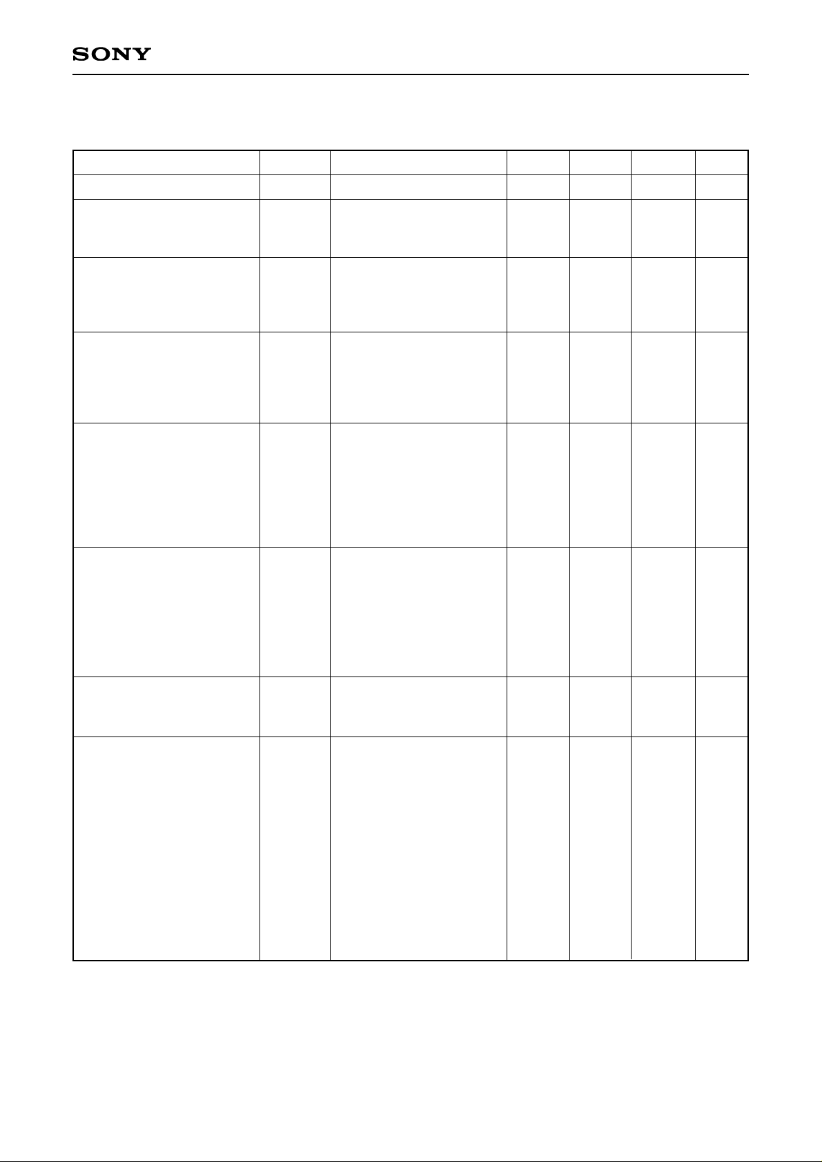
Resolution
DC characteristics
Integral linearity error
Differential linearity error
Analog input
Analog input capacitance
Analog input resistance
Analog input current
Reference input
Reference resistance
Reference current
Offset voltage VRT side
VRB side
Digital input (ECL, PECL)
Digital input voltage: High
: Low
Threshold voltage
Digital input current: High
: Low
Digital input capacitance
Digital input (TTL)
Digital input voltage: High
: Low
Threshold voltage
Digital input current: High
: Low
Digital input capacitance
Digital output (TTL)
Digital output voltage
: High
: Low
Switching characteristics
Maximum conversion rate
Aperture jitter
Sampling delay
Clock high pulse width
Clock low pulse width
Reset signal setup time
Reset signal hold time
Clock output delay
Data output delay
Output rise time
Output fall time
Electrical Characteristics
( AVCC, DVCC1, 2,DGND3 = +5V, AGND,DGND1, 2,DVEE3 = 0V, VRT = 4V, VRB = 2V, Ta = 25°C)
Item Symbol Min. Typ. Max. UnitConditions
EIL
EDL
CIN
RIN
IIN
Rref
∗
2
Iref
∗
3
EOT
EOB
VIH
VIL
VTH
IIH
IIL
VIH
VIL
VTH
IIH
IIL
VOH
VOL
Fc
Taj
Tds
Tpw1
Tpw0
T_rs
T_rh
Td_clk
Tdo1
Tdo2
Tr
Tf
7
0
400
2.7
6
0
DVEE3 + 1.5
DVEE3 + 1.1
–50
–50
2.0
–10
–20
2.4
160
1.2
2.5
2.9
1.0
–0.5
3.0
3.5
8
10
15
100
600
3.3
8
1.5
DGND3 – 1.2
1.5
10
1.3
4.0
T
∗
4
+ 0.5
4.5
1
1
±0.5
±0.5
35
285
740
5.0
10
3
DGND3
VIH – 0.4
20
20
5
0.8
5
0
5
0.5
1.5
6.5
7.0
bits
LSB
LSB
pF
kΩ
µA
Ω
mA
mV
mV
V
V
V
µA
µA
pF
V
V
V
µA
µA
pF
V
V
MSPS
ps
ns
ns
ns
ns
ns
ns
ns
ns
ns
ns
VIN = 2Vp-p, Fc = 5MSPS
VIN = +3.0V + 0.07Vrms
VIH = DGND3 – 0.8V
VIL = DGND3 – 1.6V
VIH = 3.5V
VIL = 0.2V
IOH = –2mA
IOL = 1mA
DMUX mode
CLK
CLK
RESETN – CLK
RESETN – CLK
(CL = 5pF)
DMUX mode (CL = 5pF)
(CL = 5pF)
0.8 to 2.0V (CL = 5pF)
0.8 to 2.0V (CL = 5pF)
∗
These characteristics are for PECL input unless otherwise specified.
Page 9
– 9 –
CXA3276Q
∗
4
T =
∗
5
TPS: Times Per Sample
∗
6
Pd = (ICC + IEE) · VCC +
(VRT – VRB)
2
Rref
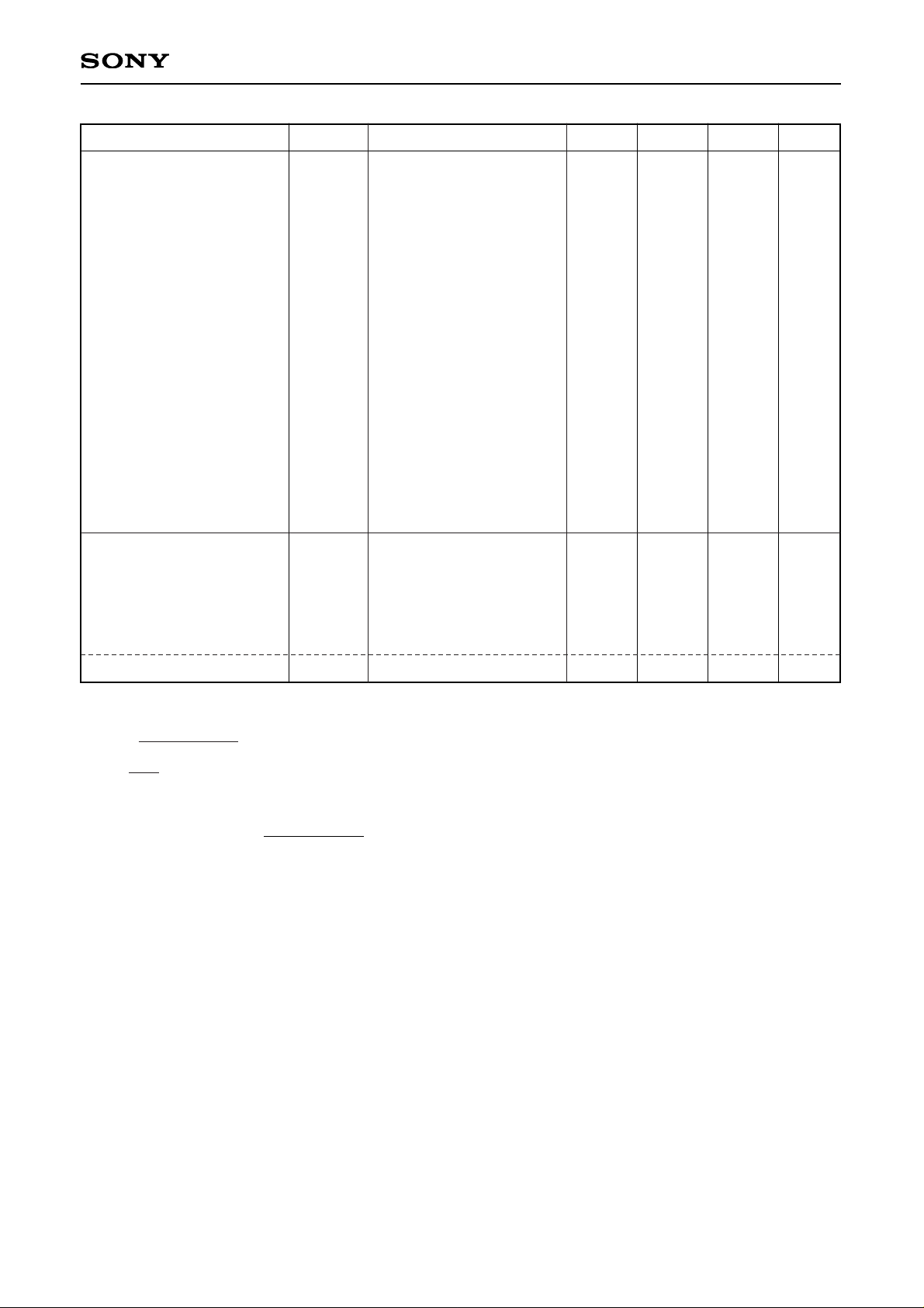
Dynamic characteristics
Input bandwidth
S/N ratio
Error rate
Power supply
Supply current
AVcc pin supply current
DVcc1 pin supply current
DVcc2 pin supply current
DGND3 pin supply current
Power consumption
ICC + IEE
AICC
DICC1
DICC2
IEE
Pd
∗
6
250
89
62
22
4.0
0.5
480
46
42
108
550
10
–12
2 × 10
–8
10
–9
140
87
36
15
1.5
700
MHz
dB
dB
TPS
∗5
TPS
TPS
mA
mA
mA
mA
mA
mW
VIN = 2Vp-p, –3dB
Fc = 160MSPS,
fin = 1kHz Fs
DMUX mode
Fc = 160MSPS,
fin = 9.999MHz Fs
DMUX mode
Fc = 160MSPS,
fin = 1kHz Fs
DMUX mode
Error > 16LSB
Fc = 160MSPS,
fin = 9.999MHz Fs
DMUX mode
Error > 16LSB
Fc = 125MSPS,
fin = 31.249MHz Fs
Straight mode
Error > 16LSB
{
{
{
{
{
1
Fc
Item Symbol Min. Typ. Max. UnitConditions
∗
2
Rref: Resistance value between VRT and VRB
∗
3
Iref =
VRT – VRB
Rref
Page 10

– 10 –
CXA3276Q
Table 1. I/O Correspondence Table
INV
1
D7 D0 D7 D0
0
VIN
VRT
VRM2
VRB
255
254
.
.
.
128
127
.
.
.
1
0
1 1 1 1 1 1 1 1
1 1 1 1 1 1 1 0
.
.
.
1 0 0 0 0 0 0 0
0 1 1 1 1 1 1 1
.
.
.
0 0 0 0 0 0 0 1
0 0 0 0 0 0 0 0
0 0 0 0 0 0 0 0
0 0 0 0 0 0 0 1
.
.
.
0 1 1 1 1 1 1 1
1 0 0 0 0 0 0 0
.
.
.
1 1 1 1 1 1 1 0
1 1 1 1 1 1 1 1
Step
Page 11
– 11 –
CXA3276Q
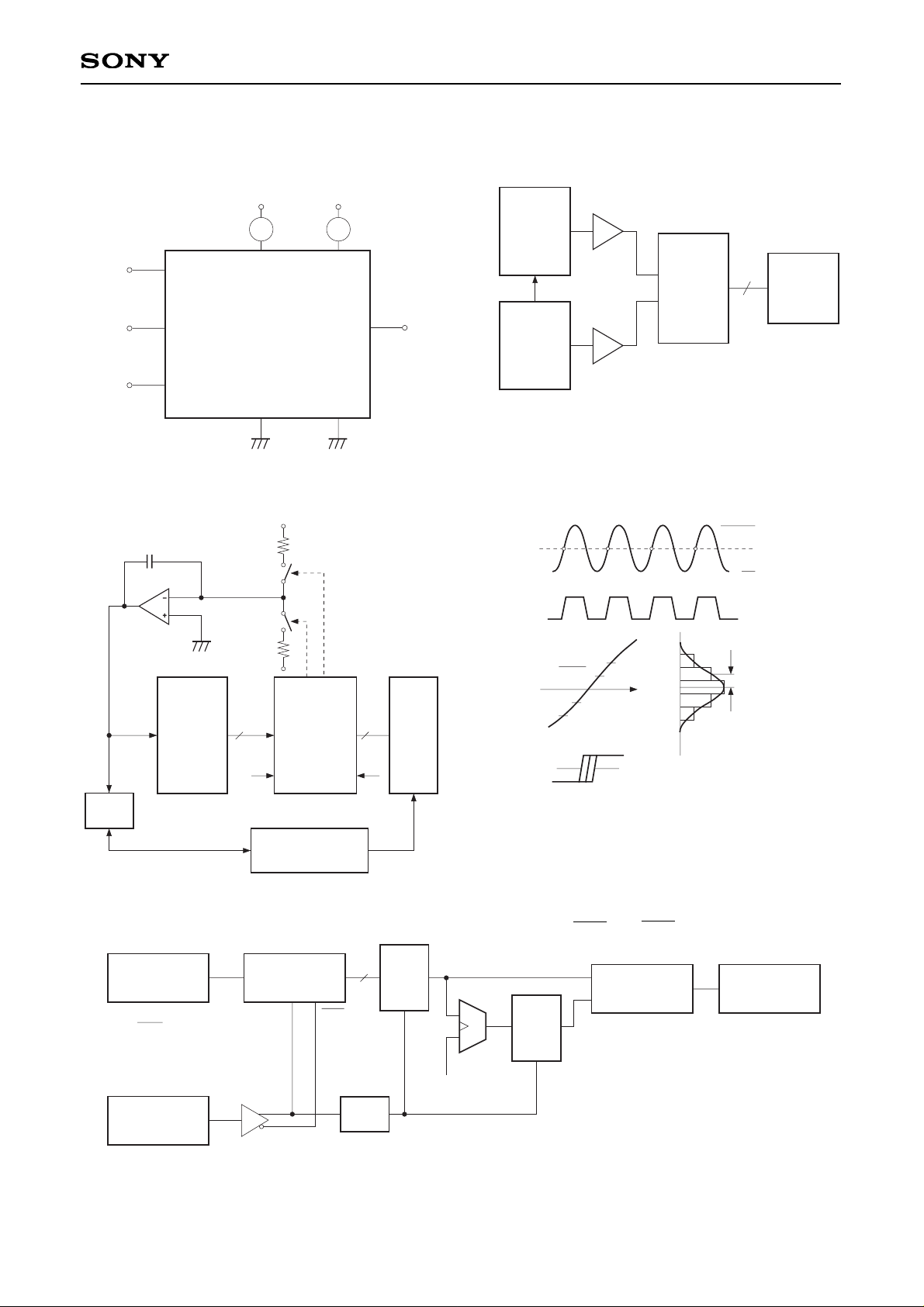
Electrical Characteristics Measurement Circuit
Current Consumption Measurement Circuit
VRT
VIN
VRB
AVCC
DVCC1
DVCC2
DGND3
DGND2
DGND1
AGND
CLK/E
DV
EE3
A A
5MHz PECL
4V
1.95V
2V
5V 5V
Icc
I
EE
Integral Linearity Error Measurement Circuit
Differential Linearity Error Measurement Circuit
CXA3276Q
A < B A > B
Comparator
A8
to
A1
A0
B8
to
B1
B0
Buffer
Controller
DVM
8 8
“1”“0”
000 ··· 00
to
111 ··· 10
V
IN
+V
–V
S2
S1
S1: ON when A < B
S2: ON when A > B
Sampling Delay Measurement Circuit
Aperture Jitter Measurement Circuit
CXA3276Q
OSC1
φ: Variable
OSC2
Logic
Analiyzer
100MHz
100MHz
Amp
ECL
Buffer
CLK
V
IN
8
fr
1024
samples
Aperture Jitter Measurement Method
VIN
σ (LSB)
CLK
V
IN
CLK
∆υ
∆ t
VRT
VRM2
V
RB
129
128
127
126
125
Sampling timing fluctuation
(= aperture jitter)
Error Rate Measurement Circuit
Comparator
A > B
Pulse
Counter
CXA3276Q
Signal
Source
Latch
Latch
1/N
+
Signal
Source
Fc
N
– 1kHz
2Vp-p Sin Wave
Fc
V
IN
CLK CLK
8
16LSB
A
B
Where σ (LSB) is the deviation of the output codes when
the largest slew rate point is sampled at the clock which
has exactly the same frequency as the analog input
signal, the aperture jitter Taj is:
Taj = σ/ = σ/ ( )
∆t
∆υ
2
256
× 2πf
Page 12

– 12 –
CXA3276Q
Description of Operation Modes
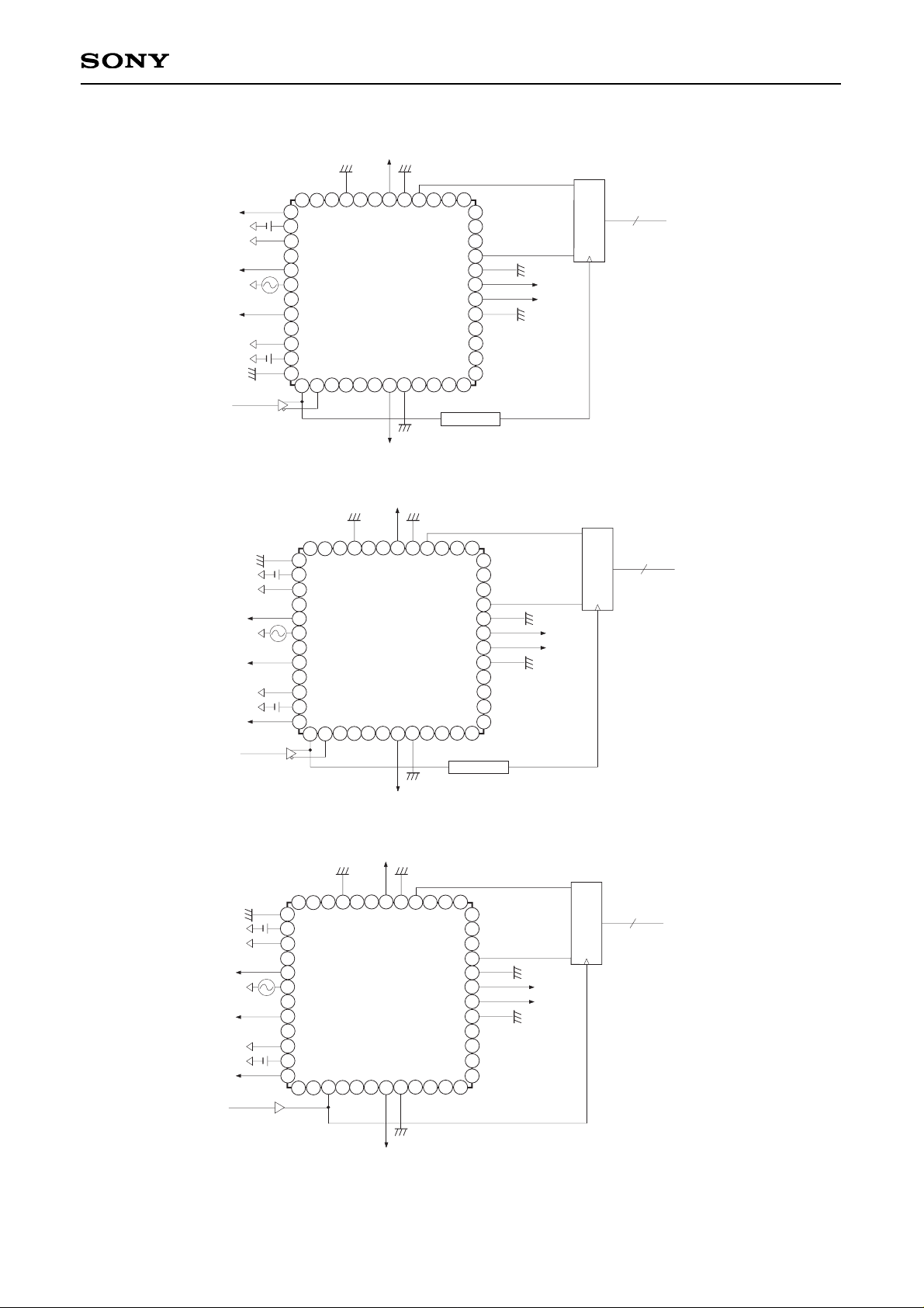
The CXA3276Q has two types of operation modes which are selected with Pin 45 (SELECT).
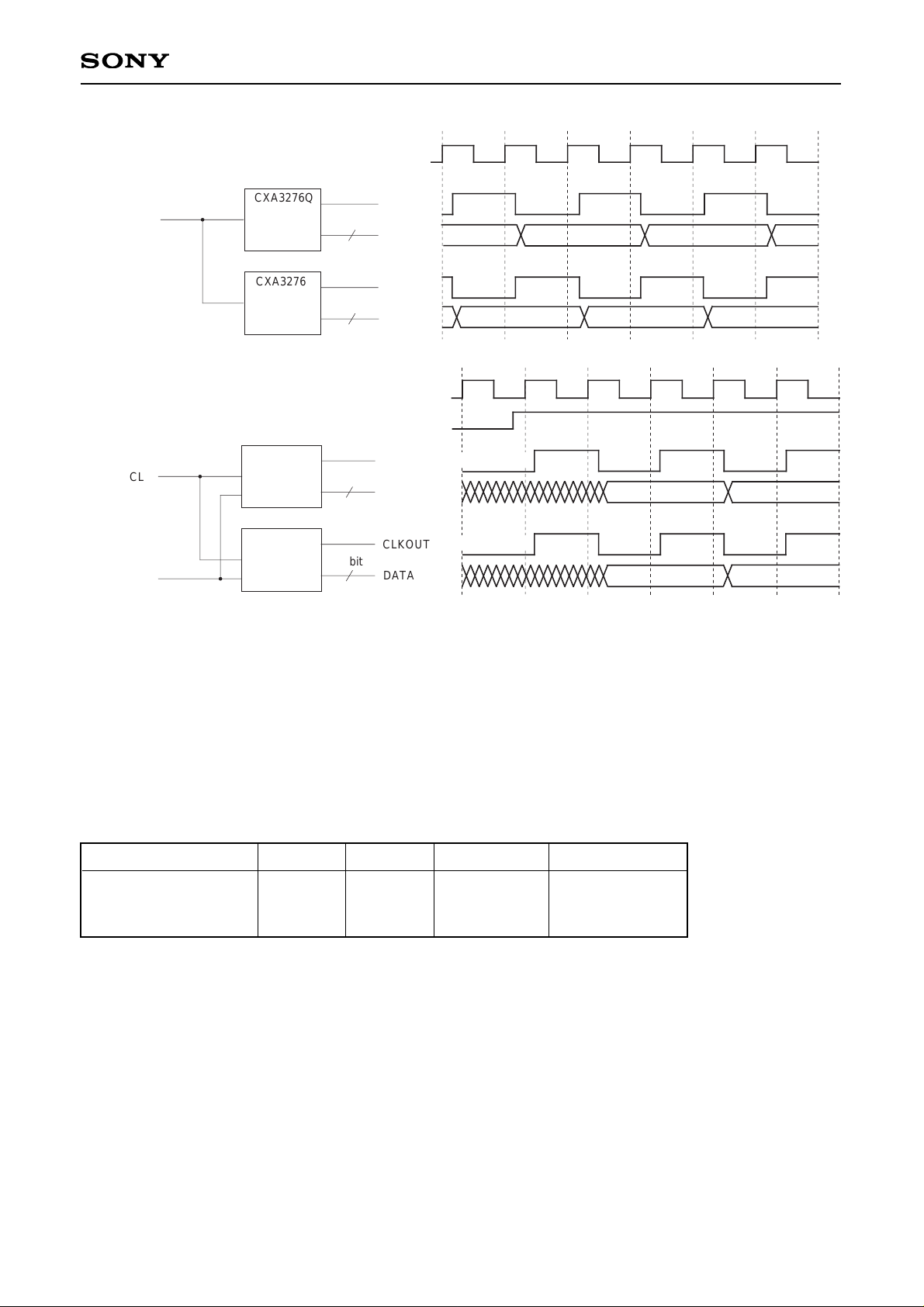
1. DMUX mode (See Application Circuit 1-(1), (2) and (3).)
Set the SELECT pin to Vcc for this mode. In this mode, the clock frequency is divided by 2 in the IC, and the
data is output after being demultiplexed by this 1/2 frequency-divided clock. The 1/2 frequency-divided clock,
which has adequate setup time and hold time for the output data, is output from the clock output pin.
When using the multiple CXA3276Q in DMUX mode, the start timing of the 1/2 frequency-divided clocks
becomes out of phase, producing operation such as that shown in the example on the next page. As a
countermeasure, the CXA3276Q has a function that resets the 1/2 frequency-divided clocks.
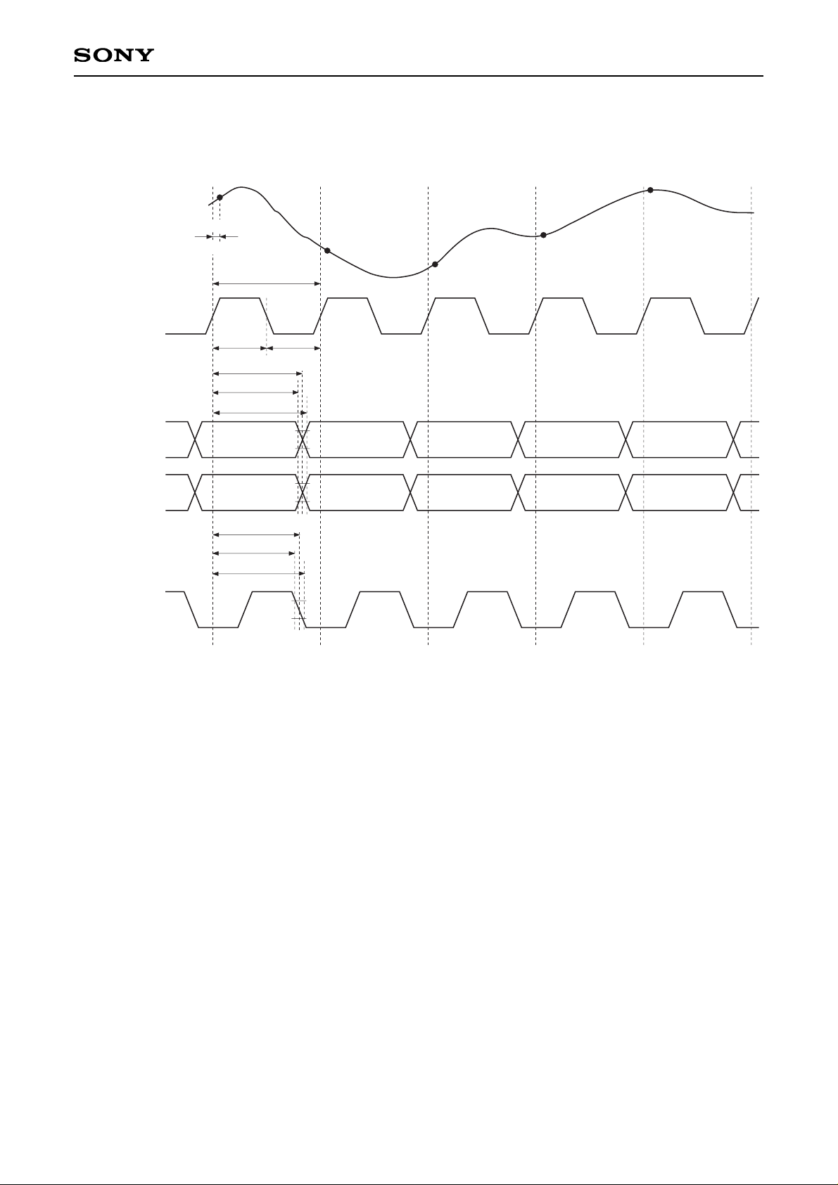
When resetting this 1/2 frequency-divided clock, the low level of the reset signal should be input to the
RESETN pin (Pin 46 or 48). The reset signal requires the setup time (T_rs ≥ 1.0ns) and hold time (T_rh ≥
–0.5ns) to the clock rising edge because it is synchronized with and taken in the clock.
The reset period can be extended by making the low level period of the reset signal longer because the clock
output pin is fixed to low (reset) during the low level period at the clock rising edge. If the reset start timing is
regarded as not important, the timing where the reset signal is set from high to low is not so consequence.
However, when the reset is released the timing where the reset signal is set from low to high must become
significant because the timing is used to commence the 1/2 frequency-divided clock. In this case, the setup
time (T_rs) is also necessary.
See the timing chart for detail. (This chart shows the example of reset for 2T.)
The A/D converter can operate at Fc (min.) = 160MSPS in this mode.
Table 2. Operation Mode Table
SELECT1
pin
VCC
GND
DMUX mode
Straight mode
160MSPS
125MSPS
Demultiplexed output
80Mbps
Straight output
125Mbps
The input clock is 1/2 frequency divided
and output. 80MHz
The input clock is inverted and output.
125MHz
Operation
mode
Maximum
conversion rate
Data output Clock output
Page 13
– 13 –
CXA3276Q
8bit
CLKOUT
DATA
8bit
CLKOUT
DATA
CLK
A
B
CLK
A
CXA3276Q
CXA3276Q
CLK
RESETN
CLK
RESETN
A
B
A
8bit
CLKOUT
DATA
8bit
CLKOUT
DATA
CLK
CXA3276Q
CXA3276Q
A
B
CLK
RESETN
CLK
RESETN
CLK
Reset signal
Reset signal
(Reset period)
(Reset period)
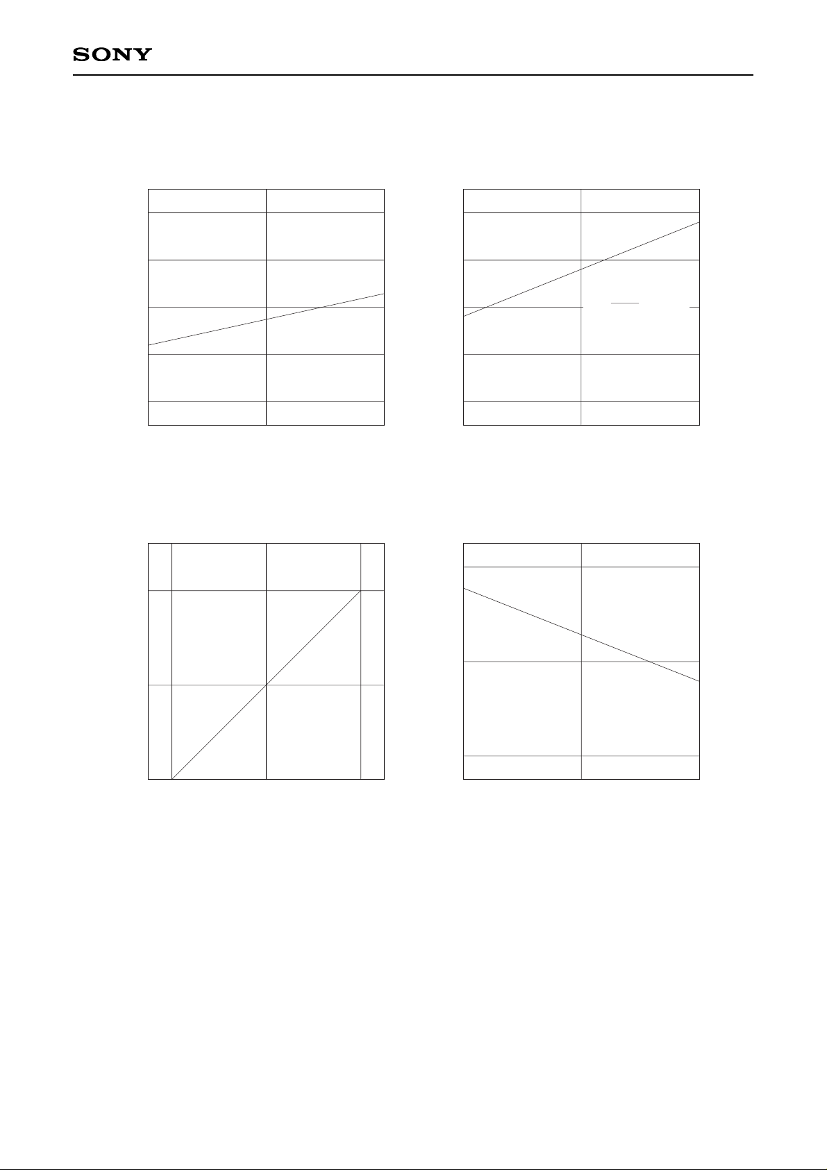
2. Straight mode (See Application Circuits 1-(4), (5) and (6).)
Set the SELECT pin to GND for this mode. In this mode, data output can be obtained in accordance with the
clock frequency applied to the A/D converter for applications which use the clock applied to the A/D converter
as the system clock.
The A/D converter can operate at Fc (min.) = 125MSPS in this mode.
Digital input level and supply voltage settings
The logic input level for the CXA3276Q supports ECL, PECL and TTL levels.
The power supplies (DVEE3, DGND3) for the logic input block must be set to match the logic input (CLK and
reset signals) level.
Digital input level
ECL
PECL
TTL
–5V
0V
0V
0V
+5V
+5V
±5V
+5V
+5V
(1) (4)
(2) (5)
(3) (6)
DVEE3 DGND3 Supply voltage Application circuits
Table 3. Logic Input Level and Power Supply Settings
When the reset signal is not used
When the reset signal is used
A
A
Page 14

– 14 –
CXA3276Q
Application Circuit 1
(1) DMUX ECL input
+5V (D)
DG
–5V (D)
AG
DG
+5V (A)
4V
+5V (D)
DG
8 bit Digital Data
Latch
8 bit Digital Data
Latch
PBD0 to PBD7
8 bit Digital Data
PAD0 to PAD7
8 bit Digital Data
ECL RESET signal
ECL-CLK
DG
3
4
5
6
7
8
9
10
11
12
13
14
15
16
17
18
19
20
21
22
23
24
25
26
27
28
29
30
40
39
38
37
36
35
34
31
32
33
41
42
43
44
45
46
47
48
1
DG
+5V (D)
2V
+5V (A)
2
AGAGAGAG
(2) DMUX PECL input
+5V (D)
DG
+5V (D)
DG
8 bit Digital Data
Latch
8 bit Digital Data
Latch
PBD0 to PBD7
8 bit Digital Data
PAD0 to PAD7
8 bit Digital Data
PECL-CLK
DG
3
4
5
6
7
8
9
10
11
13
14
15
16
17
18
19
20
21
22
23
24
25
26
27
28
29
30
40
39
38
37
36
35
34
31
32
33
41
42
43
44
45
46
47
48
1
DG
+5V (D)
2
+5V (D)
AG
DG
+5V (A)
4V
2V
+5V (A)
AGAGAGAG
PECL RESET signal
12
(3) DMUX TTL input
+5V (D)
DG
AG
AG
+5V (A)
4V
+5V (D)
DG
8 bit Digital Data
Latch
8 bit Digital Data
Latch
PBD0 to PBD7
8 bit Digital Data
PAD0 to PAD7
8 bit Digital Data
TTL RESET signal
TTL-CLK
DG
3
4
5
6
7
8
9
10
11
13
14
15
16
17
18
19
20
21
22
23
24
25
26
27
28
29
30
40
39
38
37
36
35
34
31
32
33
41
42
43
44
45
46
47
48
1
DG
+5V (D)
2V
AG
+5V (A)
2
+5V (D)
DG
AGAG
12
Page 15
– 15 –
CXA3276Q
(4) Straight ECL input
+5V (D)
DG
+5V (D)
DG
8 bit Digital Data
Latch
PBD0 to PBD7
8 bit Digital Data
ECL-CLK
DG
3
4
5
6
7
8
9
10
11
12
13
14
15
16
17
18
19
20
21
22
23
24
25
26
27
28
29
30
40
39
38
37
36
35
34
31
32
33
41
42
43
44
46
47
48
1
DG
+5V (D)
2
ECL → TTL
DG
45
AGAG
+5V (A)
4V
2V
AG
+5V (A) –5V (D)
DG
AGAG
(5) Straight PECL input
+5V (D)
DG
+5V (D)
DG
8 bit Digital Data
Latch
PBD0 to PBD7
8 bit Digital Data
PECL-CLK
DG
3
4
5
6
7
8
9
10
11
12
13
14
15
16
17
18
19
20
21
22
23
24
25
26
27
28
29
30
40
39
38
37
36
35
34
31
32
33
41
42
43
44
46
47
48
1
DG
+5V (D)
2
PECL → TTL
DG
45
AGAG
+5V (A)
4V
2V
AG
+5V (A)
+5V (D)
DG
AGAG
(6) Straight TTL input
+5V (D)
DG
+5V (D)
DG
TTL-CLK
DG
3
4
5
6
7
8
9
10
11
12
13
14
15
16
17
18
19
20
21
22
23
24
25
26
27
28
29
30
40
39
38
37
36
35
34
31
32
33
41
42
43
44
46
47
48
1
DG
+5V (D)
2
DG
45
AGAG
+5V (A)
4V
2V
AG
+5V (A)
+5V (D)
DG
AGAG
8 bit Digital Data
Latch
PBD0 to PBD7
8 bit Digital Data
Page 16
– 16 –
CXA3276Q
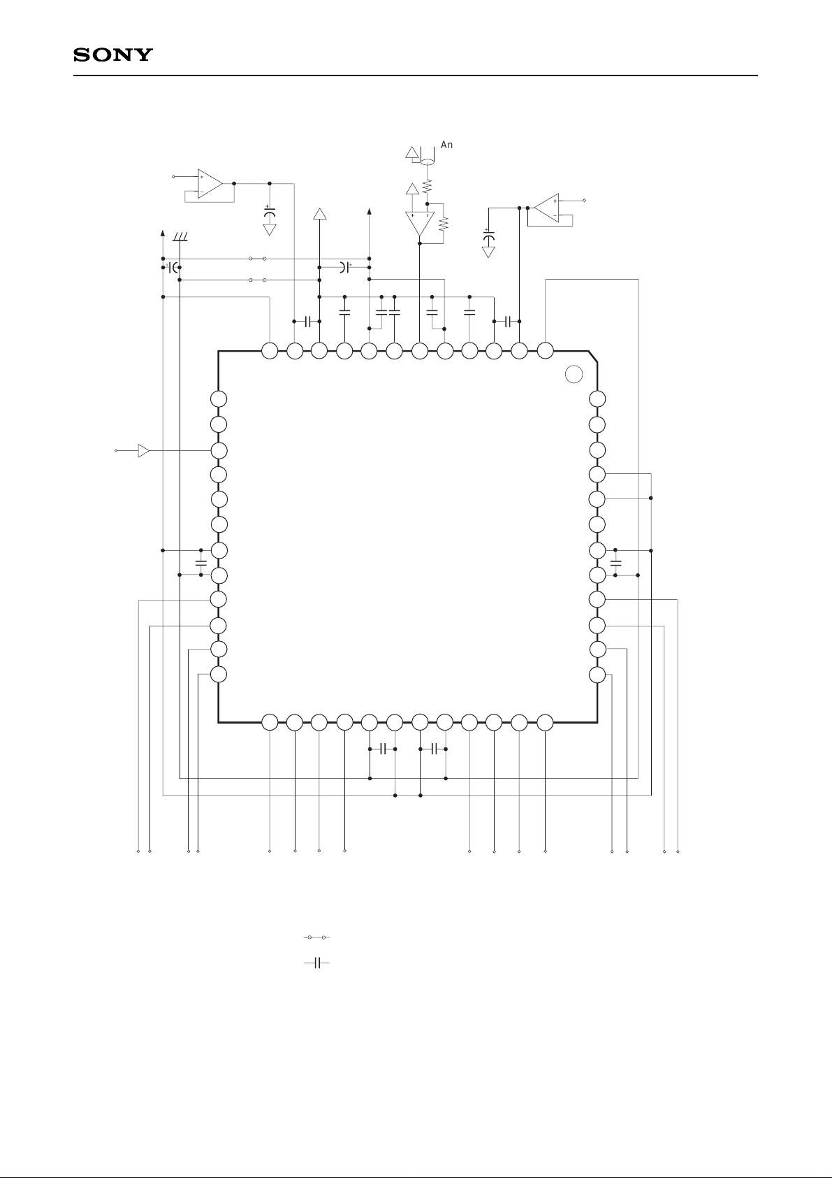
Application Circuit 2 DMUX Mode TTL I/O (When a single power supply is used)
CLK/E
N.C.
CLK/T
N.C.
N.C.
DV
CC2
DGND2
PAD0
PAD1
PAD2
PAD3
CLKN/E
RESETN/E
SELECT
RESETN/T
INV
CLKOUT
DV
CC2
DGND2
PBD7
PBD6
PBD5
PBD4
RESET/E
DV
EE
3
V
RM
1
AGND
AV
CC
V
IN
V
RM
2
AV
CC
V
RM
3
AGND
V
RT
DGND3
V
RB
PAD4
PAD7
PAD6
DV
CC
1
DV
CC
2
DGND2
PBD0
PBD1
PBD2
PBD3
PAD5
DGND1
Analog
input
AG
+5V (A)
2V
4V
TTL CLK
(LSB) PAD0
PAD1
PAD2
PAD3
PAD4
PAD5
PAD6
(MSB) PAD7
(LSB) PBD0
(MSB) PBD7
PBD1
PBD2
PBD3
PBD4
PBD5
PBD6
1µF
10µF
10µF
1µF
2
3
4
5
6
7
8
9
10
11
12
13
14
15
16
17
18
19
20
21
22
23
25
26
27
28
29
30
40
39
38
37
36
35
34
31
32
33
41
42
43
44
45
46
47
48
1
AG
AG
DG
+5V
(D)
AG
AG
24
short
short
Short the analog system and digital system at one point immediately
under the A/D converter. See the Notes on Operation.
is the chip capacitor of 0.1µF. Also, C∗ is important to suppress the noise generated
during the TTL output circuit is operating. Place C∗ at the fixed position
between the pins with the shortest distance.
C
∗
C
∗
C
∗
Application circuits shown are typical examples illustrating the operation of the devices. Sony cannot assume responsibility for
any problems arising out of the use of these circuits or for any infringement of third party patent and other right due to same.
Page 17

– 17 –
CXA3276Q
DMUX Mode Timing Chart (Select = VCC)
CLK
V
IN
T
Tpw0Tpw1
N + 2
N + 3
N + 1
N + 4
N + 5
N
N + 6
Tds
1.3ns (typ.)
N – 1
N – 2
2.0V
0.8V
N + 1
2.0V
0.8V
Tdo1
≈T ≈T
PBD0 to D7
PAD0 to D7
N
N + 2
N + 3
CLK OUT
RESETN
T_rs
T_rhT_rsT_rh
2.0V
0.8V
(Reset period)
2.0V
0.8V
Tdo2; 4.5ns (typ.)
Td_clk; 4.0ns (typ.)
2.0V
A
0.8V
T + 0.5ns (typ.)
3.5ns (min)
7.0ns (max)
3.0ns (min)
(Pin 6)
(Pin 13)
(Pin 21 to 28)
(Pin 33 to 40)
(Pin 43)
(Pin 48)
6.5ns (max)
Page 18
– 18 –
CXA3276Q
Straight Mode Timing Chart (Select = GND)
Tds
T
Tpw1
N + 1
N – 1
N
N + 2
N + 3
CLK
V
IN
Tpw0
1.3ns (typ.)
N – 2 N
PBD0 to D7
N + 1N – 1N – 3
2.0V
0.8V
PAD0 to D7
N – 3 N – 1
N N – 2N – 4
2.0V
0.8V
CLK OUT
(CLK is inverted
and output.)
2.0V
0.8V
Td_clk; 4.0ns (typ.)
Tdo2; 4.5ns (typ.)
6.5ns (max)
3.0ns (min)
3.5ns (min)
7.0ns (max)
(Pin 6)
(Pin 13)
(Pin 21 to 28)
(Pin 33 to 40)
(Pin 43)
Page 19

– 19 –
CXA3276Q
Notes on Operation
• The CXA3276Q has the PECL and TTL input pins for the clock and reset input pins. When the clock is input
in PECL level, inputting the reset signal in PECL level is recommended. Also, when the clock is input in TTL
level, inputting the reset signal in TTL is recommended.
• The impedance of the input signal should be properly matched to ensure the CXA3276Q's stable operation at
high speed.
• The power supply and grounding have a profound influence on converter performance. The power supply
and grounding method are particularly important during high-speed operation. General points for caution are
as follows.
— The ground pattern should be as large as possible. It is recommended to make the power supply and
ground patterns wider at an inner layer using a multi-layer board.
— To prevent interference between AGND and DGND and between AVcc and DVcc, make sure the
respective patterns are separated. To prevent a DC offset in the power supply pattern, connect the AVcc
and DVcc lines at one point each via a ferrite-bead filter, etc. Shorting the AGND and DGND patterns in
one place immediately under the A/D converter improves A/D converter performance.
— Be sure to turn the analog and digital power supplies on simultaneously. If not simultaneously, the IC does
not operate correctly.
— Ground the power supply pins (AVcc, DVcc1, DVcc2, DVEE3) as close to each pin as possible with a
0.1µF or larger ceramic chip capacitor.
(Connect the AVcc pin to the AGND pattern and the DVcc1, DVcc2 and DVEE3 pins to the DGND pattern.)
— It is recommended to place the ceramic chip capacitor of 0.1µF or more, in particular, between DVcc2
and DGND2 with the shortest distance.This has the effect to suppress the noise generated when the
CXA3276Q TTL output circuit operates.
— The digital output wiring should be as short as possible. If the digital output wiring is long, the wiring
capacitance will increase, deteriorating the output slew rate and resulting in reflection to the output
waveform since the original output slew rate is quite fast.
• The analog input pin VIN has an input capacitance of approximately 10pF. To drive the A/D converter with the
proper frequency response, it is necessary to prevent performance deterioration due to parasitic capacitance
or parasitic inductance by using a large capacity drive circuit, keeping wiring as short as possible, and using
chip parts for resistors and capacitors, etc.
• The VRT and VRB pins must have adequate by-pass to protect them from high-frequency noise. By-pass them
to AGND with approximately 1µF tantal capacitor and 0.1µF chip capacitor as short as possible.
• If the CLKN/E pin is not used, by-pass this pin to DGND with an approximately 0.1µF capacitor. At this time,
approximately DGND3 – 1.2V voltage is generated. However, this is not recommended for use as the threshold
voltage VBB because it is too weak.
• When the digital input level is ECL or PECL level,
∗∗∗
/E pins should be used and
∗∗∗
/T pins left open. When
the digital input level is TTL,
∗∗∗
/T pins should be used and
∗∗∗
/E pins left open.
• The CXA3276Q TTL output high level is clamped to approximately 2.8 V in the IC.This makes it possible to
directly interface with the 3.3V system CMOS IC.
• The CXA3026AQ has the output pins P1∗∗and P2∗∗. However, in the CXA3276Q, these symbols are
changed as PA∗∗and PB∗∗. At this time, the P1 side of the CXA3026AQ is changed to the PB side for the
CXA3276Q; the P2 side of the CXA3026AQ to the PA side for the CXA3276Q.
• The pipeline delay of the CXA3276Q is smaller by one clock, compared to that of CXA3026AQ.
Page 20
– 20 –
CXA3276Q
Current consumption vs.
Ambient temperature characteristics
Ta – Ambient temperature [°C]
–25
100
25 75
Current consumption [mA]
105
110
115
120
Current consumption vs.
Conversion rate characteristics
Fc – Conversion rate [MSPS]
0
100
80
Current consumption [mA]
105
110
115
120
160
fin = – 1kHz
fCLK
4
DMUX mode
CL = 5pF
Analog input current vs.
Analog input voltage characteristics
Analog input voltage [V]
2 3 4
Analog input current [µA]
50
100
0
Reference current vs.
Ambient temperature characteristics
Ta – Ambient temperature [°C]
–25
2
25 75
Reference current [mA]
3
4
V
RT = 4V
VRB = 2V
Example of Representative Characteristics
Page 21

– 21 –
CXA3276Q
SNR vs. Input frequency response
Input frequency [MHz]
1
20
5 50
SNR [dB]
30
40
50
303 10
Error rate vs. Conversion rate characteristics
120 140 160
10
–5
10
–6
10
–7
10
–8
10
–9
Maximum conversion rate vs.
Ambient temperature characteristics
Ta – Ambient temperature [°C]
–25
140
25 75
Fc – Maximum conversion rate [MSPS]
160
180
150
170
Fc = 160MSPS
Error Rate [TPS]
Fc – Conversion rate [MSPS]
Error > 16LSB
f
CLK
16
fin = – 1kHz
180
fin = – 1kHz
fCLK
16
Error > 16LSB
Error rate: 2 × 10⁻⁸ TPS
Page 22
– 22 –
CXA3276Q
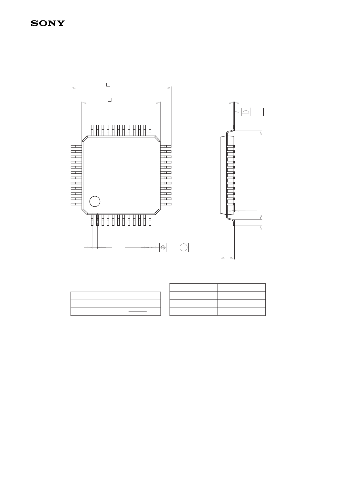
Package Outline Unit: mm
SONY CODE
EIAJ CODE
JEDEC CODE
M
PACKAGE STRUCTURE
PACKAGE MATERIAL
LEAD TREATMENT
LEAD MATERIAL
PACKAGE MASS
EPOXY RESIN
SOLDER / PALLADIUM
PLATING
42/COPPER ALLOY
48PIN QFP (PLASTIC)
15.3 ± 0.4
12.0 – 0.1
+ 0.4
0.8
0.3 – 0.1
+ 0.15
0.24
13
24
2536
37
48
1 12
2.2 – 0.15
+ 0.35
0.9 ± 0.2
0.1 – 0.1
+ 0.2
13.5
0.15 – 0.05
+ 0.1
QFP-48P-L04
QFP048-P-1212
0.7g
0.15
NOTE : PALLADIUM PLATING
This product uses S-PdPPF (Sony Spec.-Palladium Pre-Plated Lead Frame).
 Loading...