

Page 1
CXA3268AR
Driver/Timing Generator for Color LCD Panels
Description
The CXA3268AR is an IC designed to drive the color
LCD panels ACX300, ACX301, ACX302 and ACX703.
This IC greatly reduces the number of peripheral
circuits and parts by incorporating a RGB driver and
timing generator for video signals onto a single chip.
This chip has a built-in serial interface circuit and
electronic attenuators which allow various settings to
be performed by microcomputer control, etc.
Features
• Color LCD panel ACX300, ACX301, ACX302 and
ACX703 driver
• Supports NTSC and PAL systems
• Supports 16:9 wide display (letter box and pulse
elimination display)
• Supports Y/color difference and RGB inputs
• Supports OSD input (digital input)
• Power saving function
• Serial interface circuit
• Electronic attenuators (D/A converter)
• Trap and LPF (f0, fc variable)
• COMMON and PSIG output circuits
• Sharpness function
• 2-point γ correction circuit
• R, G, B signal delay time adjustment circuit
• D/A output pin (0 to 3V, 8 level output)
• Output polarity inversion circuit
• Supports AC drive for LCD panel during no signal
Applications
Compact LCD monitors, etc.
Absolute Maximum Ratings (Ta = 25°C)
• Supply voltage VCC16 V
VCC215 V
VCC315 V
VDD 5.5 V
• Analog input pin voltage
VINA (Pins 57, 58 and 59)
GND – 0.3 to VCC1 + 0.3 V
VINA (Pins 3, 69) VCC1V
VINA (Pin 30) 1.5 to VCC2 – 4 V
VINA (Pin 71) 0.9 Vp-p
VINA (Pins 70, 72) 0.8 Vp-p
• Digital input pin voltage
VIND (other than Pins 5, 10, 14, 15 and 16)
VSS – 0.3 to VDD + 0.3 V
VIND (Pins 5, 10) VSS – 0.3 to +5.5 V
• Common input pin voltage
VINAD (Pins 14, 15 and 16)
GND, VSS – 0.3 to +5.5 V
• Operating temperature
Topr –15 to +75 °C
• Storage temperature
Tstg –55 to +150 °C
• Allowable power dissipation
PD (Ta ≤ 25°C) 737 mW
Operating conditions
• Supply voltage
VCC1 – GND1 2.7 to 3.6 V
VCC2 – GND2 11.0 to 14.0 V
VCC3 – GND3 11.0 to 14.0 V
VDD – Vss 2.7 to 3.6 V
• Input voltage
SIG.C voltage
VSIG.C 5.0 to 6.5 V
RGB input signal voltage (Pins 70, 71 and 72)
∗1
VRGB 0 to 0.7 (0.5 typ.) Vp-p
Y input signal voltage (Pin 71)
∗2
VY 0 to 0.5 (0.35 typ.) Vp-p
R-Y input voltage (Pin 72)
∗2
VR-Y 0 to 0.49 (0.245 typ.) Vp-p
B-Y input voltage (Pin 70)
∗2
VB-Y 0 to 0.622 (0.311 typ.) Vp-p
∗1
During RGB input
∗2
During Y/color difference input
– 1 –
E99529B98-PS
Sony reserves the right to change products and specifications without prior notice. This information does not convey any license by
any implication or otherwise under any patents or other right. Application circuits shown, if any, are typical examples illustrating the
operation of the devices. Sony cannot assume responsibility for any problems arising out of the use of these circuits.
72 pin LQFP (Plastic)
Page 2
– 2 –
CXA3268AR
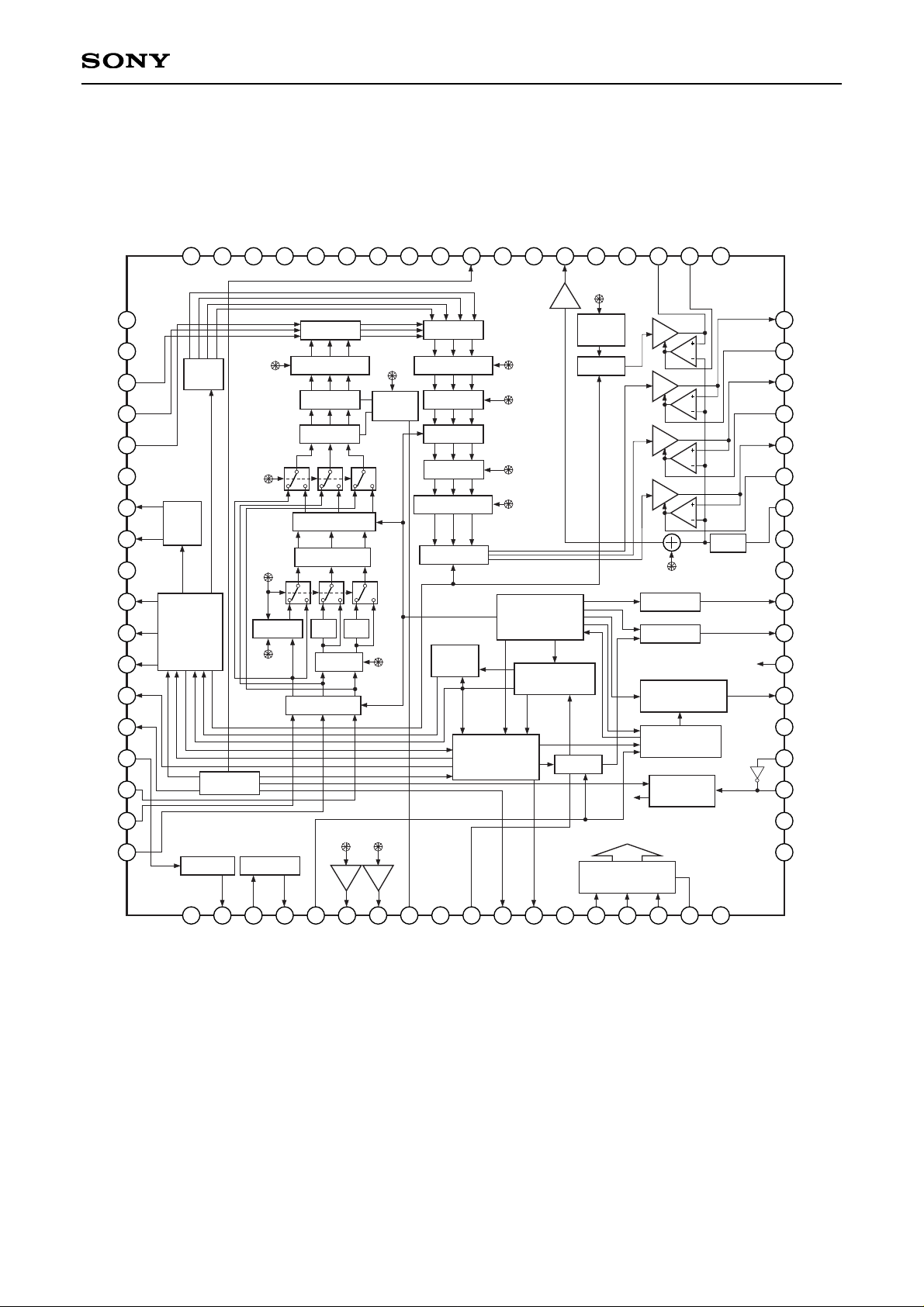
Block Diagram
1 2 3 4 5 6 7 8 9 10 11 12
13 14
15 16 17 18
19
20
21
22
23
24
25
26
27
28
29
30
31
32
33
34
35
36
37
38394041424344454647484950515253
54
55
56
57
58
59
60
61
62
63
64
65
66
67
68
69
70
71
72
Vss
FIL OUT
SYNC IN
SYNC OUT
CSYNC/HD
DA OUT
REF
F ADJ
GND1
VD
DWN
WIDE
TST1
SCK
SEN
SDAT
R INJECT
V
SS
G OUT
G DC DET
R OUT
R DC DET
B OUT
B DC DET
SIG.C
GND2
GND2
TST2
HDO
VDO
XCLR
RPD
Vss
CKI
CKO
V
DD
VDD
+3.0V
+3.0V
+3.0V
+3.0V
Vss
VssGND1Vss
MCK
V
DD
TST11
OSD B
OSD R
OSD G
NC
HCK1
HCK2
Vcc1
HST
EN
VCK
VST
RGT
FIL IN
B/B-Y
G/Y
DA
R/R-Y
Vss
Vss
TST10
TST9
TST8
TST7
TST6
TST5
NC
POF
TST4
GND3
COM
Vcc3
TST3
PSIG OUT
PSIG DC DET
Vcc2
CLK
CLP
Buf
+12.0V+12.0VGND3Vss Vss
S/P CONV
REGISTER DAC
PHASE
COMPARATOR
PLL
COUNTER
HSYNC DET
H SKEW DET
V CONTROL
V POSITION
PULSE
ELM
H.FILTER SYNC SEP
POL SW
MODE
HDO GEN
VDO GEN
S/H
S/H
GEN
HCK
GEN
OSD RGB
TRAP
LPF
CLAMP
FILTER
BIAS
HCOUNTER
HPULSE
GEN
POL SW
GAMMA
CLAMP
BLK-LIM
USER-BRIGHT
G R B
SUB-BRIGHT
CK
CONTROL
PSIGBRIGHT
Buf
PSIGBRT
U-BRT
MODE
LPF
FILTER
PIC-G
HUE
COLOR
PIC-F
CONT
SUB-BRT R
SUB-BRT B
γ 1 γ 2
WHITLIM
SUB-CONT R
SUB-CONT B
BLKLIM
COM-DC
REF
Buf
Buf
Buf
Buf
Buf
SIG.C
CONTRAST
G R B
CLAMP
MATRIX
DL1 DL1
PICTURE
HUE
V COUNTER
V SEP
Page 3
– 3 –
CXA3268AR
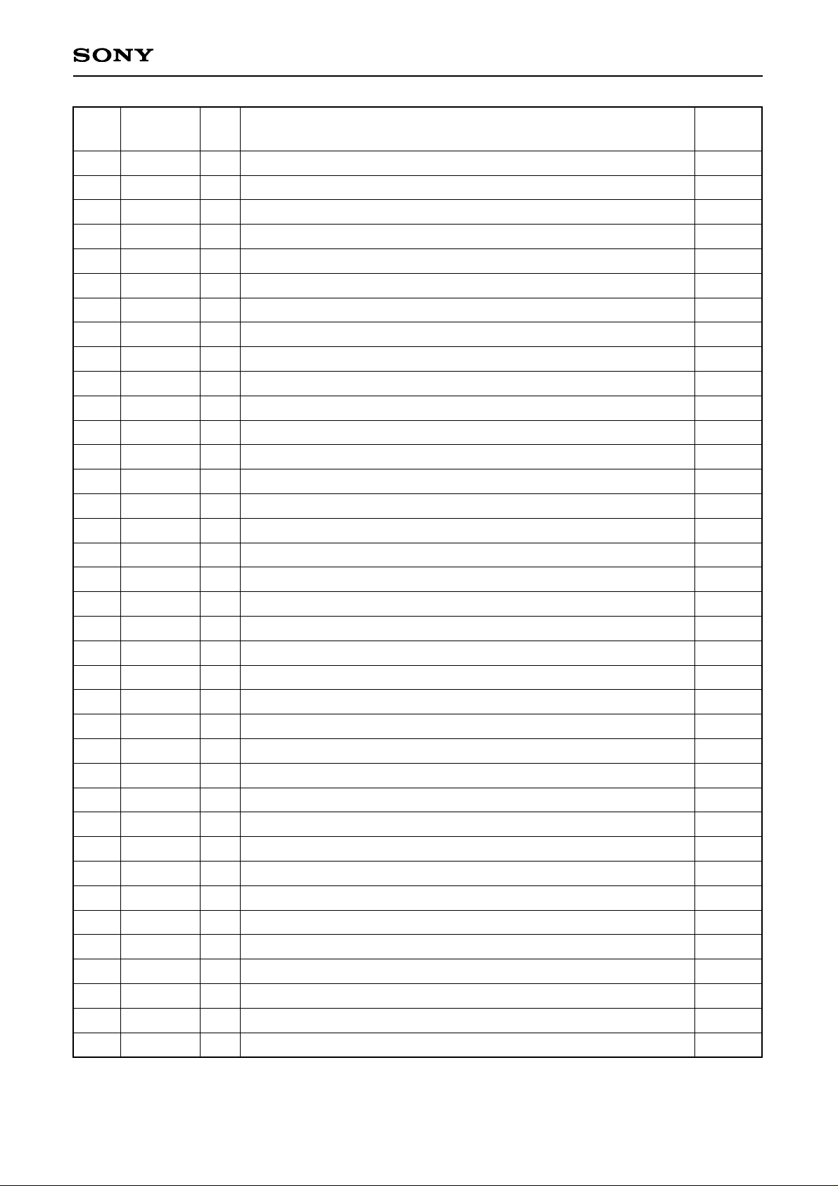
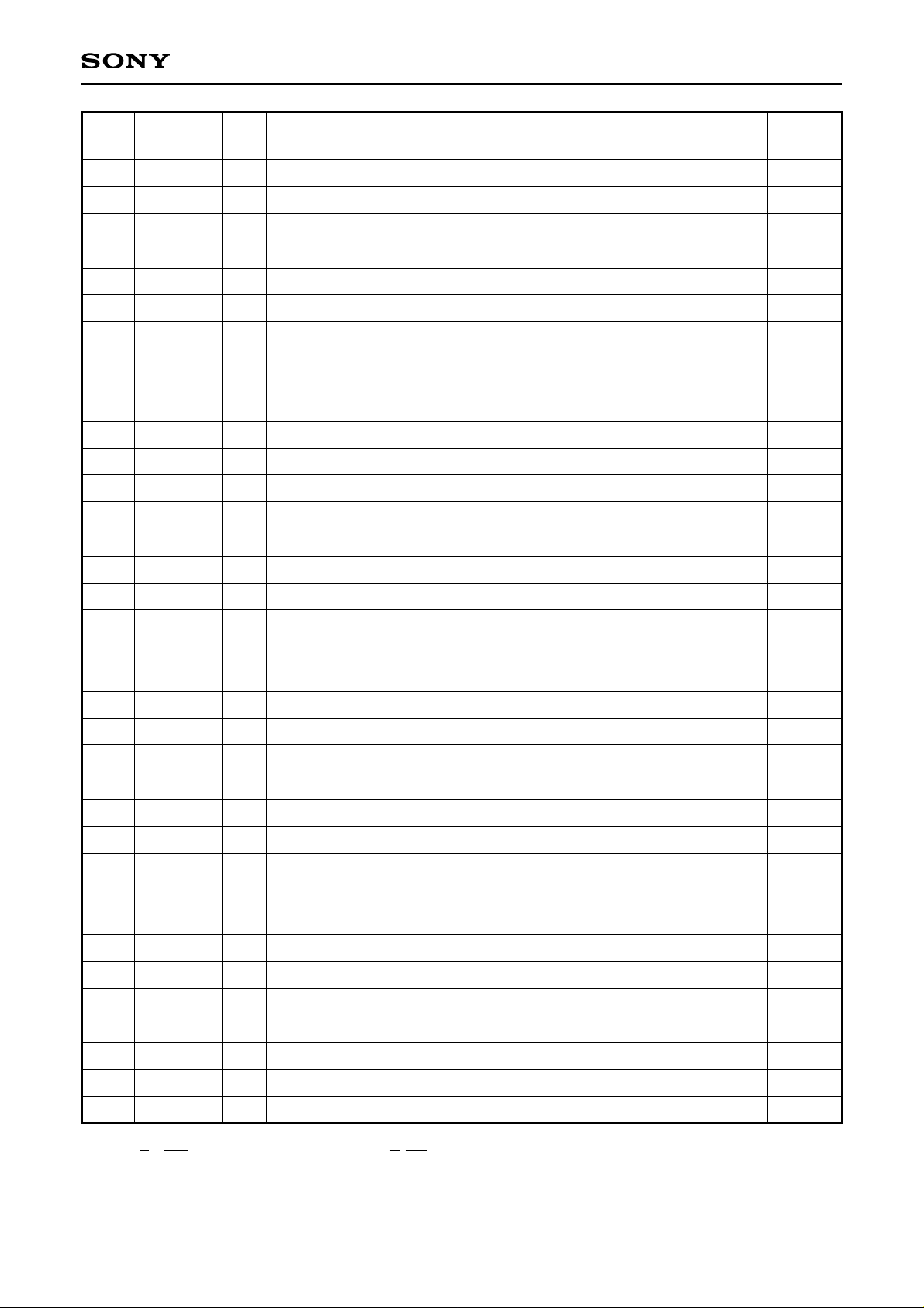
Pin Description
Pin
No.
1
2
3
4
5
6
7
8
9
10
11
12
13
14
15
16
17
18
19
20
21
22
23
24
25
26
27
28
29
30
31
32
33
34
35
36
37
VSS
FIL OUT
SYNC IN
SYNC OUT
CSYNC/HD
DA OUT
REF
F ADJ
GND1
VD
DWN
WIDE
TST1
SCK
SEN
SDAT
R INJECT
VSS
VDD
VDD
CKO
CKI
VSS
RPD
XCLR
VDO
HDO
TST2
GND2
SIG.C
B DC DET
B OUT
R DC DET
R OUT
G DC DET
G OUT
VCC2
—
O
I
O
I
O
O
O
—
I
O
O
—
I
I
I
O
—
—
—
O
I
—
O
I
O
O
—
—
I
O
O
O
O
O
O
—
Digital 3.0V GND
H filter output (for using internal sync separation)
Sync separation circuit input (for using internal sync separation)
Sync separation circuit output (for using internal sync separation)
CSYNC/horizontal sync signal input
DAC output
Level shifter circuit REF voltage output for LCD panel
Trap f0 adjusting resistor connection
Analog 3.0V GND
Vertical sync signal input
Up/down inversion switching signal output
16:9 wide display switching pulse output
Test (Leave this pin open.)
Serial clock input
Serial load input
Serial data input
Serial block current controlling resistor connection
Digital 3.0V GND
Digital 3.0V power supply
Digital 3.0V power supply
Oscillation cell output
Oscillation cell input
Digital 3.0V GND
Phase comparator output
Power-on reset capacitor connection (timing generator block)
VDO pulse output
HDO pulse output
Test (Connect to GND.)
Analog 12.0V GND
R, G, B and PSIG output DC voltage adjustment
B signal DC voltage feedback circuit capacitor connection
B signal output
R signal DC voltage feedback circuit capacitor connection
R signal output
G signal DC voltage feedback circuit capacitor connection
G signal output
Analog 12.0V power supply
L
H
Symbol I/O Description
Input pin for
open status
Page 4
– 4 –
CXA3268AR
Pin
No.
38
39
40
41
42
43
44
45
46
47
48
49
50
51
52
53
54
55
56
57
58
59
60
61
62
63
64
65
66
67
68
69
70
71
72
PSIG DC DET
PSIG OUT
TST3
VCC3
COM
GND3
TST4
POF
NC
TST5
TST6
TST7
TST8
TST9
TST10
VSS
VSS
VDD
TST11
OSD B
OSD R
OSD G
NC
HCK1
HCK2
VCC1
HST
EN
VCK
VST
RGT
FIL IN
B/B-Y
G/Y
R/R-Y
O
O
—
—
O
—
—
O
—
—
—
—
—
—
—
—
—
—
I
I
I
O
O
—
O
O
O
O
O
I
I
I
I
PSIG signal DC voltage feedback circuit capacitor connection
PSIG output
Test (Leave this pin open.)
Analog 12.0V COM (CS) power supply
Common pad voltage for LCD panel output (CS)
Analog 12.0V COM (CS) GND
Test (Leave this pin open.)
LCD panel power supply on/off (Leave this pin open when not using
this function.)
Test (Connect to GND.)
Test (Connect to GND.)
Test (Leave this pin open.)
Test (Leave this pin open.)
Test (Leave this pin open.)
Test (Leave this pin open.)
Digital 3.0V GND
Digital 3.0V GND
Digital 3.0V power supply
Test (Connect to GND.)
OSD B input
OSD R input
OSD G input
H clock pulse 1 output
H clock pulse 2 output
Analog 3.0V power supply
H start pulse output
EN pulse output
V clock pulse output
V start pulse output
Right/left inversion switching signal output
H filter input (for using internal sync separation)
B/B-Y signal input
G/Y signal input
R/R-Y signal input
Symbol I/O Description
Input pin for
open status
∗
DWN: DOWN SCAN and UP SCAN, RGT: RIGHT SCAN and LEFT SCAN
H: pull-up processing, L: pull-down processing
Page 5
– 5 –
CXA3268AR
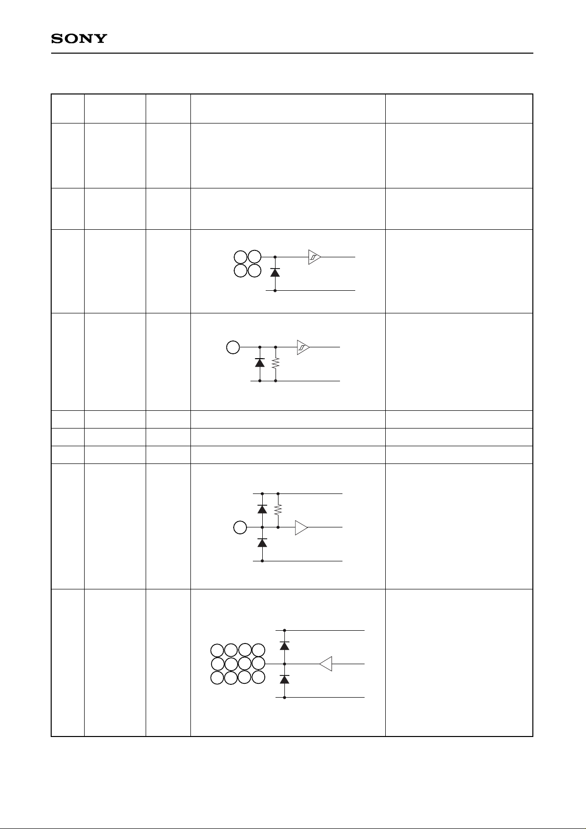
Analog Block Pin Description
Pin
No.
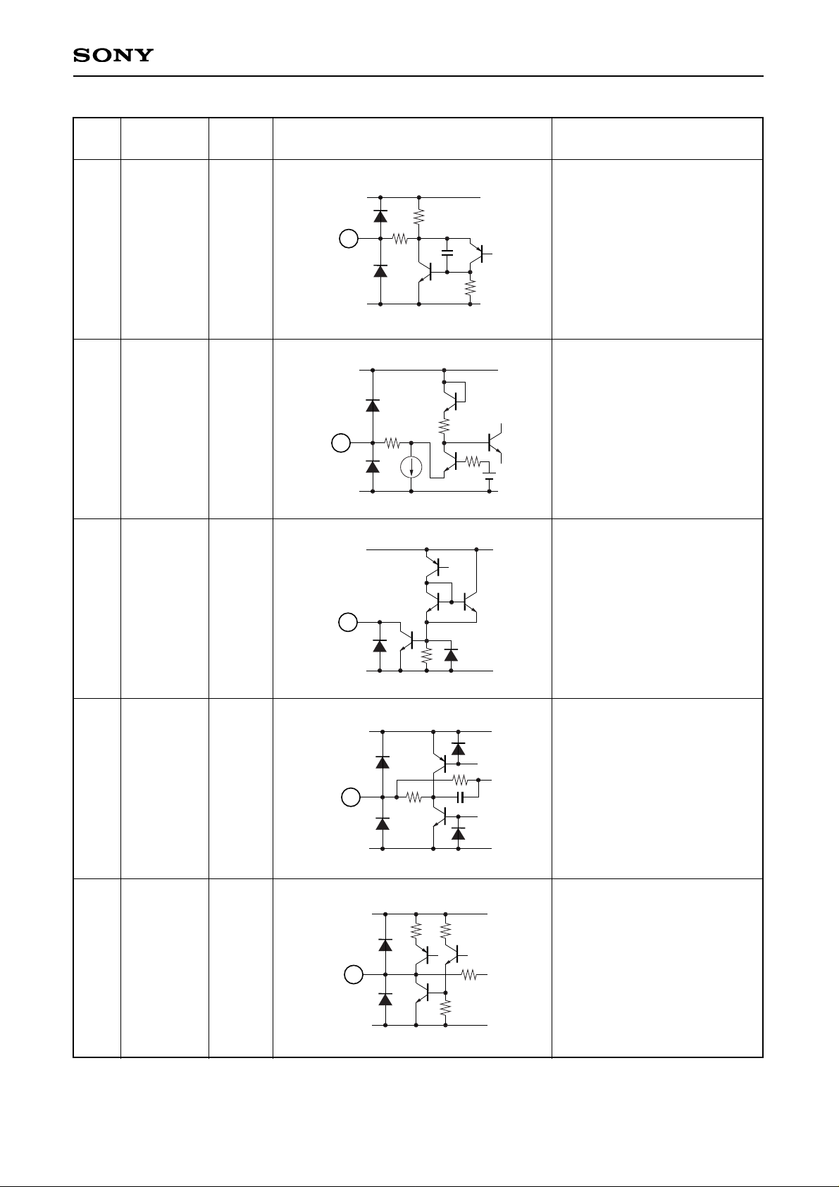
2 FIL OUT
Amplifies and outputs the sync
portion of the video signal input
to FIL IN (Pin 69).
Sync separation circuit input.
Inputs the FIL OUT (Pin 2)
output signal via a capacitor.
Sync separation output.
Positive polarity output in open
collector format.
DA output.
Outputs the serial data
converted to DC voltage. The
current driving capacity is
±1.0mA (max.).
REF output.
Outputs the serial data
converted to DC voltage. The
current driving capacity (sink)
is ±1.5mA (max.).
2.15V
1.1V
—
—
—
SYNC IN
SYNC OUT
DA OUT
REF
3
4
6
7
Symbol
Pin
voltage
Equivalent circuit Description
VCC1
23k
200
GND1
2
VCC1
200
GND1
3
VCC1
GND1
4
VCC1
50
50
GND1
6
VCC1
51k
GND1
7
Page 6
– 6 –
CXA3268AR
Pin
No.
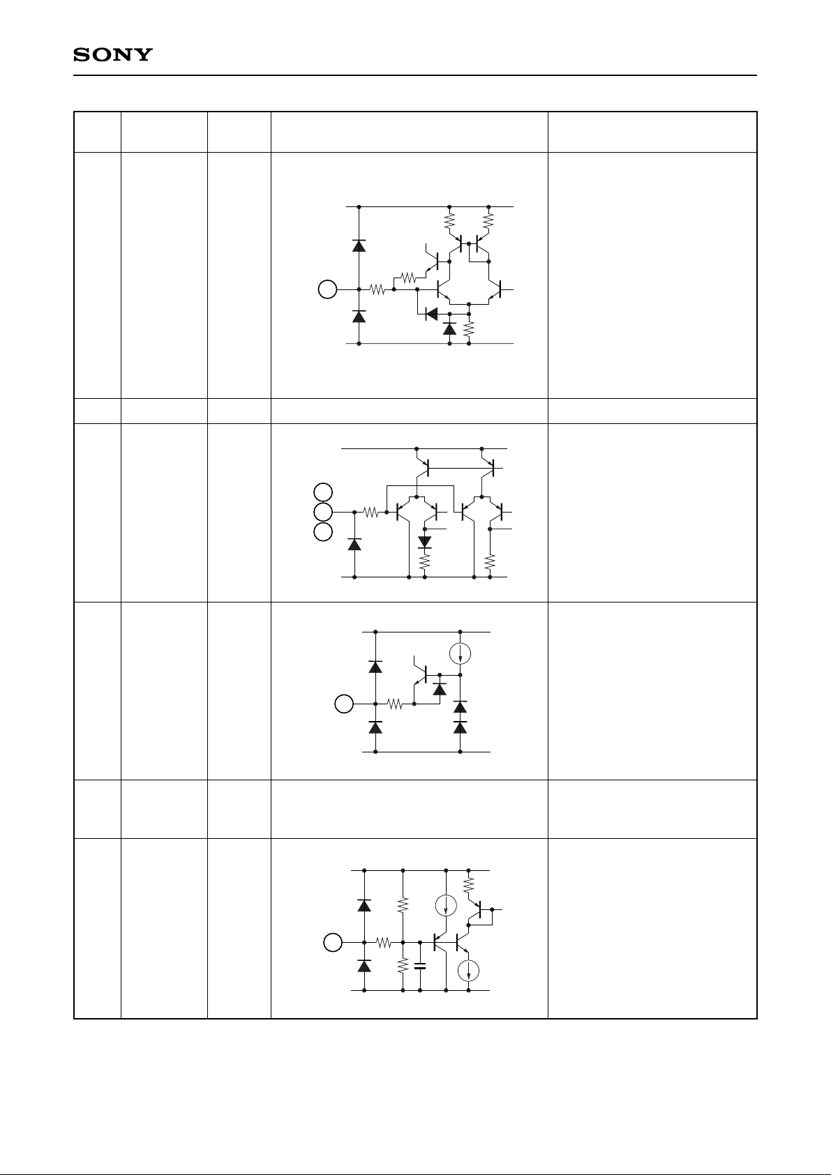
8
F ADJ
Connect a resistor between this
pin and GND1 to control the
internal LPF and trap
frequencies.
Connect a 33kΩ resistor
(tolerance ±2%, temperature
characteristics ±200ppm or less).
This pin is easily affected by
external noise, so make the
connection between the pin and
external resistor, and between
the GND side of the external
resistor and the GND1 pin as
close as possible.
Analog 3.0V GND.
1.1V
—
GND1
9
Symbol
Pin
voltage
Equivalent circuit Description
VCC1
GND1
10
6.5k
8
14
15
16
SCK
SEN
SDAT
Serial clock, serial load and
serial data inputs for serial
communication.
—
VCC1
200
GND1
14
15
16
17 R INJECT
Connect a resistor for setting
the injector current of the IIL
logic circuit. Connect a 15kΩ
resistor between this pin and
GND1. Use a resistor with a
deviation of ±2% and
temperature characteristics of
±200ppm or less.
0.7V
29
GND2
Analog 12.0V GND.
(for the RGB and PSIG output
circuits)
—
VCC1
200
GND1
17
30 SIG.C
R, G, B and PSIG output DC
voltage setting.
Connect a 0.01µF capacitor
between this pin and GND1.
When using a SIG.C of other
than VCC2/2, input the SIG.C
voltage from an external
source.
Preset
VCC2/2
Variable
range:
5.0 to 6.5V
VCC2
GND1
140k
140k
200
10p
30
Page 7
– 7 –
CXA3268AR
Pin
No.
31
33
35
38
B DC DET
R DC DET
G DC DET
PSIG DC DET
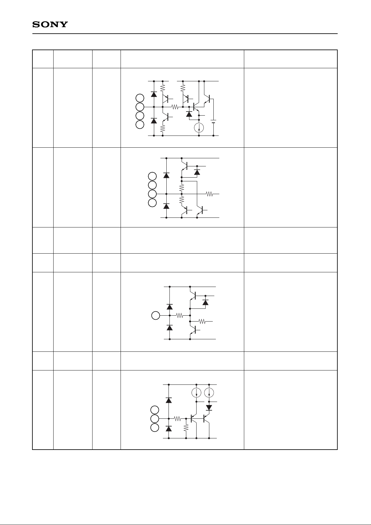
Smoothing capacitor connection
for the feedback circuit of R, G,
B and PSIG output DC level
control.
Connect a low-leakage
capacitor.
1.8V
Symbol
Pin
voltage
Equivalent circuit Description
VCC2 VCC1
200
GND1
31
33
35
38
32
34
36
39
B OUT
R OUT
G OUT
PSIG OUT
R, G, B and PSIG signal
outputs.
The DC level is controlled to
match the SIG.C pin voltage.
Low output in power saving
mode.
VCC2/2V output when preset.
VCC2/2
(SIG.C =
preset)
37
VCC2
Analog 12.0V power supply.
(for the RGB and PSIG output
circuits)
12.0V
41 VCC3
Analog 12.0V power supply.
(for COM (CS) output)
12.0V
VCC2
166k
10
10
GND2
32
34
36
39
42 COM
COMMON voltage output.
The output voltage is controlled
by serial communication.
—
VCC3
200
GND3
42
90k
57
58
59
OSD B
OSD R
OSD G
OSD pulse inputs.
When one of these input pins
exceeds the Vth1 level, all of
the outputs go to black limiter
level; when an input pin
exceeds the Vth2 level, only the
corresponding output goes to
white limiter level.
Vth1 =
VCC1 × 1/3
Vth2 =
VCC1 × 2/3
VCC1
50k
50k
GND1
57
59
58
43 GND3
Analog 12.0V GND.
(for COM (CS) output)
—
Page 8
– 8 –
CXA3268AR
Pin
No.
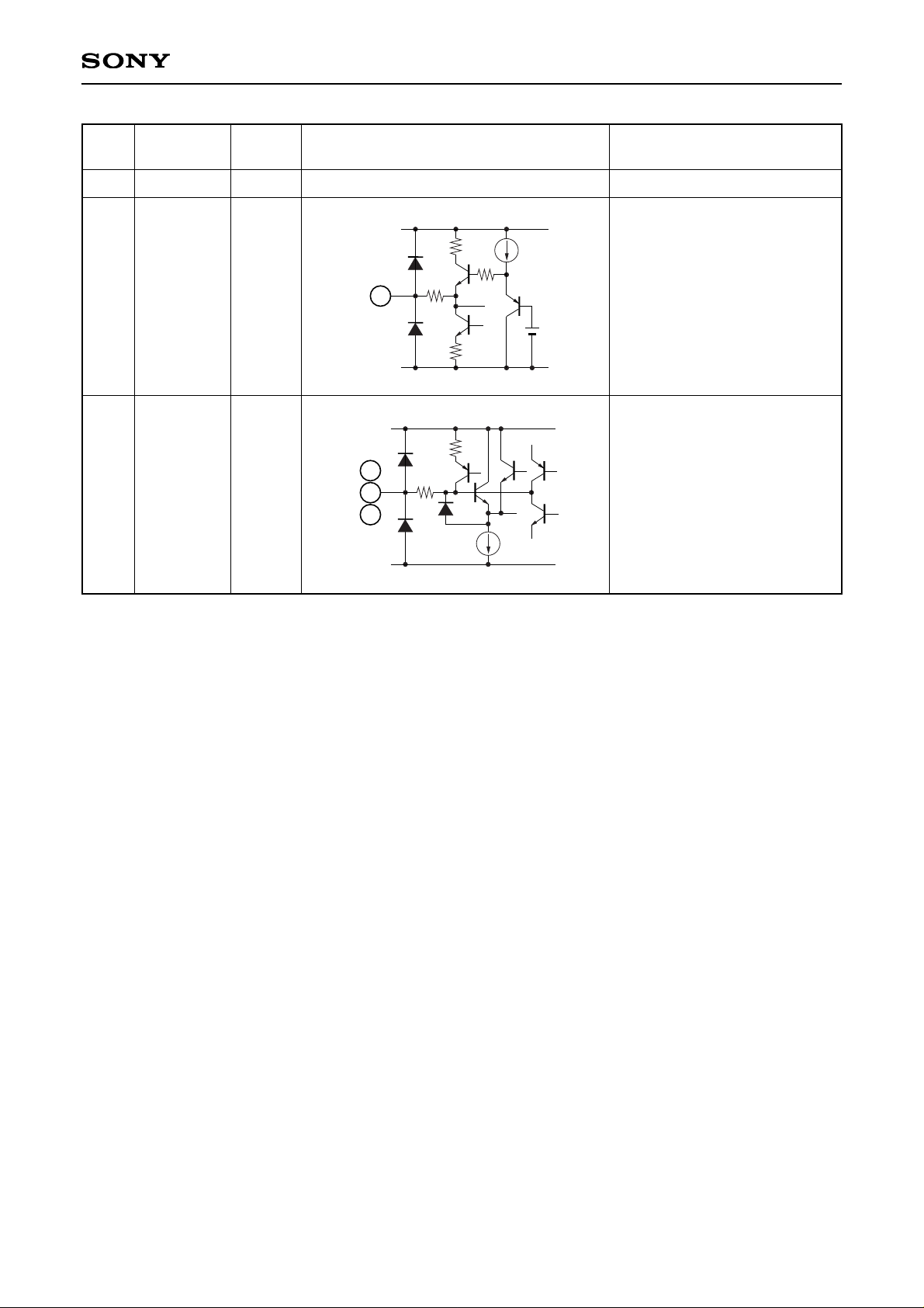
69 FIL IN
H filter input.
Input the video signal via a
capacitor.
1.2V
63
VCC1
Analog 3.0V power supply.
—
Symbol
Pin
voltage
Equivalent circuit Description
VCC1
GND1
200
69
70
71
72
B/B-Y
G/Y
R/R-Y
In Y/color difference input
mode, input the Y signal to
Pin 71, the B-Y signal to Pin 70,
and the R-Y signal to Pin 72.
In RGB input mode, input the
B signal to Pin 70, the G signal
to Pin 71 and the R signal to
Pin 72.
Pedestal clamp these pins with
external coupling capacitors.
G/Y 1.8V
R/R-Y,
B/B-Y,
RGB:
1.8V
Y/color
difference:
2.0V
VDD1
GND1
200
70
71
72
Page 9
– 9 –
CXA3268AR
Digital Block Pin Description
Pin
No.
1
18
23
53
54
VSS Digital 3.0V GND.—
19
20
55
VDD
Digital 3.0V power supply.—
5
14
15
16
CSYNC/HD
SCK
SEN
SDAT
Composite sync/horizontal sync
signal input, and serial clock,
serial load and serial data inputs
for serial communication.
—
10 VD
Vertical sync signal input.
—
21
22
24
CKO
CKI
RPD
Oscillation circuit output.
Oscillation circuit input.
Phase comparator output.
—
—
—
Symbol
Pin
voltage
Equivalent circuit Description
VSS
5
15
1614
VSS
10
VSS
VDD
25
VSS
VDD
67
66
68
11
64
65
26
27
45
61
62
12
25 XCLR Digital block system reset.—
11
12
26
27
45
61
62
64
65
66
67
68
DWN
WIDE
VDO
HDO
POF
HCK1
HCK2
HST
EN
VCK
VST
RGT
Digital block outputs.—
Page 10
– 10 –
CXA3268AR
Test Pin Description
Pin
No.
13
40
44
49
50
51
52
TST1
TST3
TST4
TST7
TST8
TST9
TST10
Test.
Leave these pins open.
—
28
47
48
56
TST2
TST5
TST6
TST11
Test.
Connect to GND.
—
Symbol
Pin
voltage
Equivalent circuit Description
Page 11
– 11 –
CXA3268AR
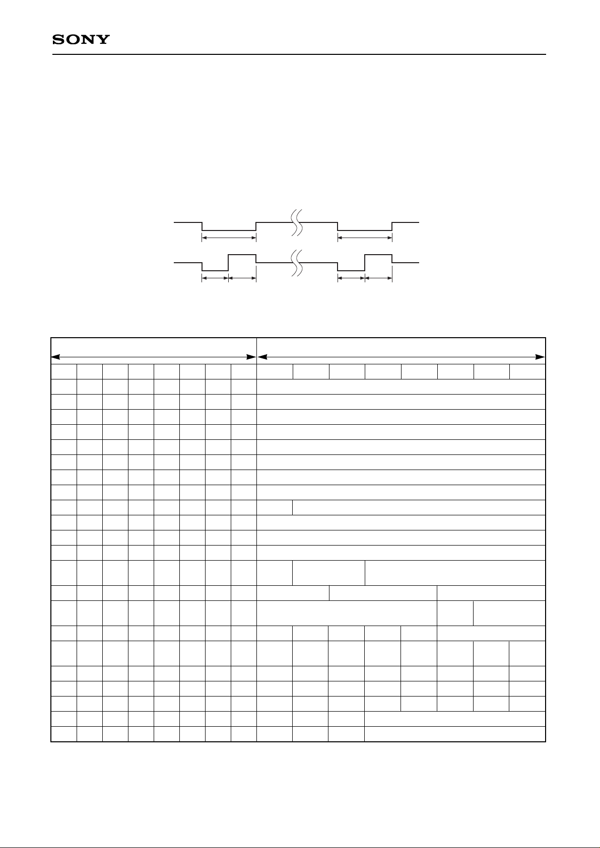
Setting Conditions for Measuring Electrical Characteristics
Use the Electrical Characteristics Measurement Circuit on page 22 when measuring electrical characteristics.
For measurement, the digital block must be initialized and power saving must be canceled by performing
Settings 1 and 2 below. In addition, the serial data must be set to the initial settings shown in the table below.
Setting 1. Horizontal AFC adjustment
Input a signal and adjust the VCO using V22 so that WL and WH of the TP24 output waveform are the same.
Setting 2. Canceling power saving mode
The power-on default is power saving mode, so clear (set all "0") serial data PS0, PS1, PS2, PS4 and SYNC GEN.
Horizontal sync
signal
RPD (Pin 24)
WS
WL WH WL WH WL = WH
WS
Fig. 1. Horizontal AFC adjustment
Serial data initial settings
Note) If there is the possibility that data may be set at other than the above-noted addresses, set these data to "0".
MSB ADDRESS LSB MSB DATA LSB
D15 D14 D13 D12 D11 D10 D9 D8 D7 D6 D5 D4 D3 D2 D1 D0
0
0
0
0
0
0
0
0
0
0
0
0
0
0
0
0
0
0
0
0
0
0
0
0
0
0
0
0
0
0
0
0
0
0
0
0
0
0
0
0
0
0
0
0
0
0
0
0
0
0
0
0
0
0
0
0
0
0
0
0
0
1
1
1
1
1
0
0
0
0
0
0
0
0
0
0
0
0
0
0
0
0
1
0
0
0
0
0
0
0
0
0
0
0
0
0
1
1
1
1
1
1
1
1
0
0
0
0
0
0
0
0
0
0
1
1
1
1
0
0
0
0
1
1
1
1
0
0
0
0
0
1
0
0
1
1
0
0
1
1
0
0
1
1
0
0
1
1
0
0
0
1
1
0
0
1
0
1
0
1
0
1
0
1
0
1
0
1
0
1
0
0
1
0
1
0
USER-BRIGHT
SUB-BRIGHT R
SUB-BRIGHT B
CONTRAST
SUB-CONTRAST R
SUB-CONTRAST B
γ-2
γ-1
0
PSIG-BRIGHT
COM-DC
COLOR
HUE
(01000110/LSB)
(10001010/LSB)
(10001010/LSB)
(00111111/LSB)
(10011111/LSB)
(10011111/LSB)
(11111111/LSB)
(11111111/LSB)
(1011111/LSB)
(10000000/LSB)
(00000000/LSB)
(10000000/LSB)
WHITE-LIMITER
(00/LSB)
BLACK-LIMITER (11111/LSB)
LPF (000/LSB)
REF (000/LSB)
FILTER (00/LSB)
PICTURE-F0
(00/LSB)
PICTURE-GAIN (00000/LSB)
0
0 0 0
MODE (1)
DA (000/LSB)
0
SLSYP (1)
0
0
0
0
0
SLEXVD (0)
SLFL (0)
0
0
0
SYNC GEN
(0)
SLDWN (0)
SLFR (0)
SLTST4 (0)
0
0
PS 4
(0)
SLRGT (0)
SL4096 (0)
SLTST3 (0)
0
SLSH2 (1)
SLCLP2 (0)
SLSH0 (1)
PS 2
(0)
SLSH1 (1)
SLCLP1 (0)
SLTST2 (0)
PS 1
(0)
SLWD (0)
SLVDP (0)
SLTST1 (0)
PS 0
(0)
SLPL (0)
SLHDP (0)
SLTST0 (0)
H-POSITION (10000)
HD-POSITION (00000)
0
0
Page 12
– 12 –
CXA3268AR
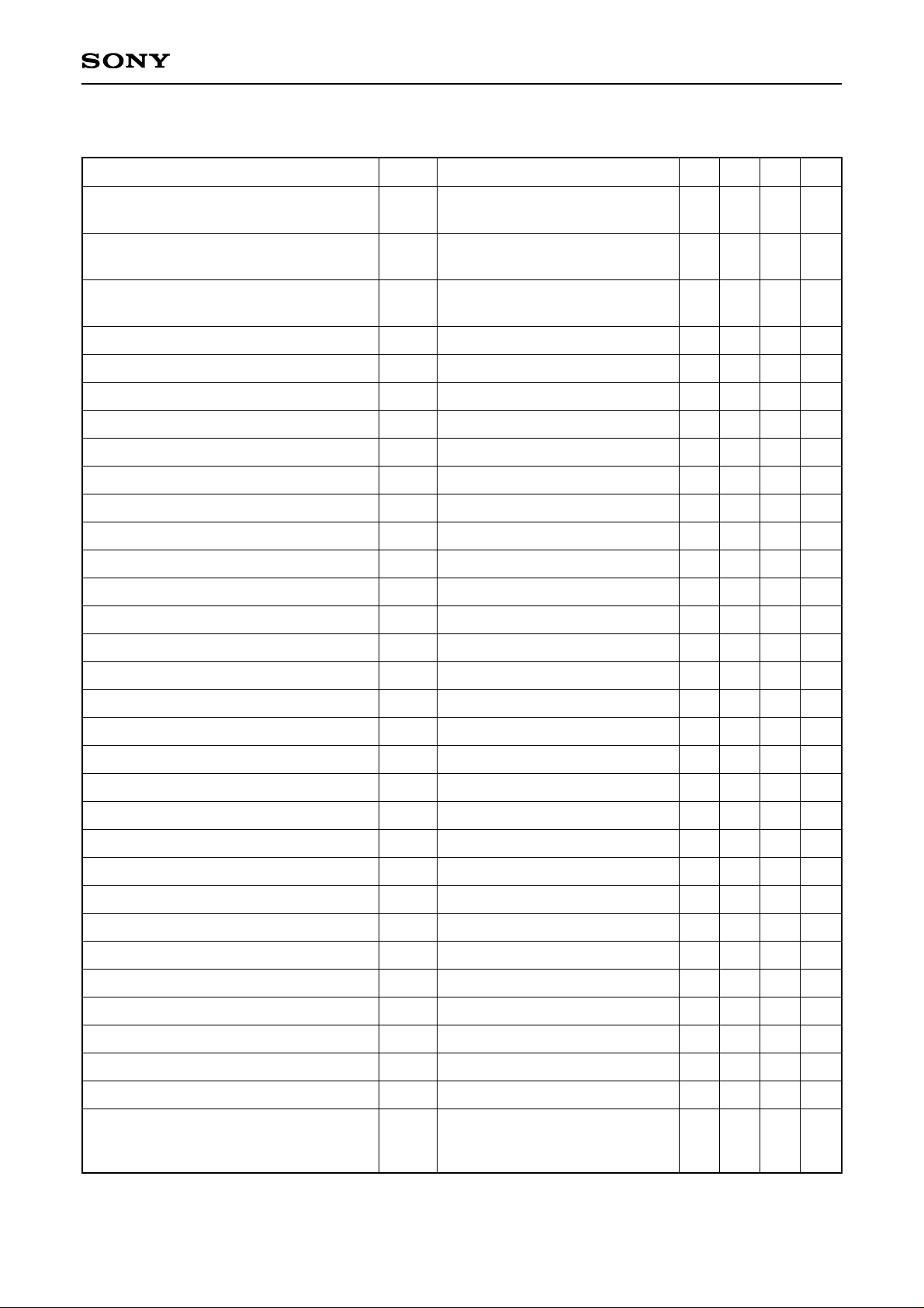
Electrical Characteristics — DC Characteristics
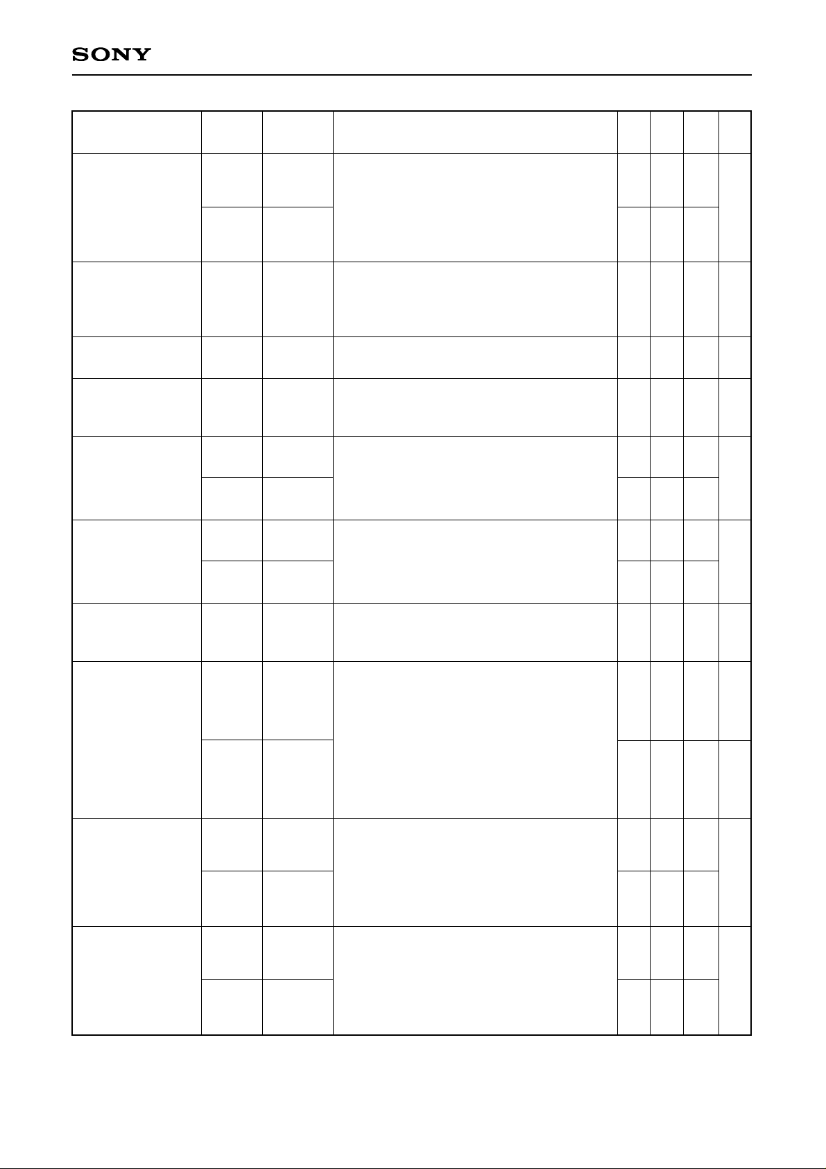
Analog Block Unless otherwise specified, Ta = 25°C, VCC1 = VDD =3.0V, VCC2/VCC3 = 12.0V,
SW4 = off for the current consumption measurement, see page 11 for the DAC.
Item
Current consumption 1
(Y/color difference input)
Current consumption 2
(Y/color difference input)
Current consumption 3
(Y/color difference input)
Current consumption 1 (RGB input)
Current consumption 2 (RGB input)
Current consumption 3 (RGB input)
Current consumption 1 (PS0 = 1)
Current consumption 2 (PS0 = 1)
Current consumption 3 (PS0 = 1)
Current consumption 1 (PS2 = 1)
Current consumption 1 (PS4 = 1)
Current consumption 1 (SYNC GEN = 1)
Current consumption 2 (SYNC GEN = 1)
Current consumption 3 (SYNC GEN = 1)
FIL OUT pin voltage
SYNC IN pin voltage
SYNC OUT pin voltage
F ADJ pin voltage
R INJECT pin voltage
SIG.C pin voltage
B DC DET pin voltage
R DC DET pin voltage
G DC DET pin voltage
PSIG DC DET pin voltage
FIL IN pin voltage
B/B-Y pin voltage 1
B/B-Y pin voltage 2
G/Y pin voltage
R/R-Y pin voltage 1
R/R-Y pin voltage 2
REF pin voltage (power saving mode)
OSD input resistance
I1
I2
I3
IRGB1
IRGB2
IRGB3
IPS01
IPS02
IPS03
IPS21
IPS41
ISG1
ISG2
ISG3
V2
V3
V4
V8
V17
V30
V31
V33
V35
V38
V69
V70
V70
V71
V70
V70
V7
V57
V58
V59
Measure the inflow current to Pin 63.
Measure the inflow current to Pin 37.
Measure the inflow current to Pin 41.
Measure the inflow current to Pin 63.
Measure the inflow current to Pin 37.
Measure the inflow current to Pin 41.
Measure the inflow current to Pin 63.
Measure the inflow current to Pin 37.
Measure the inflow current to Pin 41.
Measure the inflow current to Pin 63.
Measure the inflow current to Pin 63.
Measure the inflow current to Pin 63.
Measure the inflow current to Pin 37.
Measure the inflow current to Pin 41.
During no input
During no input
During no input
During Y/color difference input
During RGB input
During Y/color difference input
During RGB input
I7 = 1.5mA
1.8
1.8
0.8
0.4
5.8
1.5
1.5
1.5
1.5
0.9
1.7
1.5
1.5
1.7
1.5
80
27.0
3.8
0.90
23.0
3.8
0.90
7.5
0.18
26.5
26.5
7.0
0.18
2.1
1.1
0.2
1.1
0.7
6.0
1.8
1.8
1.8
1.8
1.2
2.0
1.8
1.8
2.0
1.8
100
37.0
5.0
1.3
30.0
5.0
1.3
10.0
0.35
1.00
36.5
36.5
9.5
0.35
1.00
2.4
1.4
0.4
1.4
1.0
6.2
2.1
2.1
2.1
2.1
1.5
2.3
2.1
2.1
2.3
2.1
0.3
120
mA
mA
mA
mA
mA
mA
mA
mA
µA
mA
mA
mA
mA
µA
V
V
V
V
V
V
V
V
V
V
V
V
V
V
V
V
V
kΩ
Symbol Measurement conditions Min. Typ. Max. Unit
Page 13

– 13 –
CXA3268AR
Digital Block (including some analog block) (Ta = –15 to +75°C, VDD = VCC1 = 3.7 to 3.6V)
Item
High level input voltage
Low level input voltage
High level threshold voltage
Low level threshold voltage
Hysteresis voltage
High level threshold voltage
Low level threshold voltage
Hysteresis voltage
High level input current
Low level input current
High level input current
Low level input current
High level input current
Low level input current
High level input current
Low level input current
Low level output voltage
High level output voltage
Low level output voltage
High level output voltage
Low level output voltage
High level output voltage
Low level output voltage
High level output voltage
Output leak current
VIH
VIL
VT+1
VT–1
VT+1 – VT–1
VT+2
VT–2
VT+2 – VT–2
| IIH1 |
| IIL1 |
| IIH2 |
| IIL2 |
| IIH3 |
| IIL3 |
| IIH4 |
| IIL4 |
VOL1
VOH1
VOL2
VOH2
VOL3
VOH3
VOL4
VOH4
| IOZ |
Schmitt buffer
VI = VDD
VI = 0V
VI = VDD
VI = 0V
VI = VDD
VI = 0V
VI = VDD
VI = 0V
IOL = 1mA
IOH = –0.25mA
IOL = 2mA
IOH = –0.5mA
IOL = 4mA
IOH = –1mA
IOL = 1.5mA
IOH = –1.25mA
High impedance status
VDD × 0.7
0.6
0.4
0.6
0.2
10
10
2.6
2.6
2.6
VDD – 0.5
Symbol
Measurement
conditions
Min.
40
40
Typ.
VDD × 0.3
2.6
2.6
1.0
1.0
3.0
100
100
3.0
1.0
2.0
0.3
0.3
0.3
0.4
1.0
Max.
V
V
V
V
V
V
V
V
µA
µA
µA
µA
µA
µA
µA
µA
V
V
V
V
V
V
V
V
µA
Unit
∗1
∗2
∗3
∗4
∗5
∗6
∗7
∗8
∗9
∗10
∗11
∗12
Applicable
pins
∗1
XCLR (Pin 25), CKI (Pin 22)
∗2
CSYNC/HD (Pin 5), VD (Pin 10)
∗3
SCK (Pin 14), SEN (Pin 15), SDAT (Pin 16)
∗4
CSYNC/HD (Pin 5), CKI (Pin 22)
∗5
XCLR (Pin 25)
∗6
VD (Pin 10)
∗7
SCK (Pin 14), SEN (Pin 15), SDAT (Pin 16)
∗8
DWN (Pin 11), WIDE (Pin 12), VCK (Pin 66), VST (Pin 67), RGT (Pin 68)
∗9
RPD (Pin 24), VDO (Pin 26), HDO (Pin 27), POF (Pin 45), HST (Pin 64), EN (Pin 65)
∗10
HCK1 (Pin 61), HCK2 (Pin 62)
∗11
CKO (Pin 21). However, when measuring the output pin (CKO), the input level of the input pin (CKI) should
be 0V or VDD.
∗12
RPD (Pin 24)
Page 14

Input SG2 (50mVp-p) to TP71 and
measure the output amplitude at TP36.
Input SG2 (50mVp-p) to TP71 and
measure the output amplitude at TP36.
Assume the output amplitude at TP36 when
SG2 (0.5Vp-p) is input to TP71 as GMIN.
∆gcon = GMAX – GMIN
Assume the inverted output amplitude at
TP36 when SG2 (0.35Vp-p) is input to TP71
as Vinv, and the non-inverted output
amplitude as Vninv.
∆ginv = 20 log (Vninv/Vinv)
Input SG2 (0.35Vp-p) to TP71 (TP70, TP72),
measure the non-inverted output amplitude
at TP32, TP34 and TP36, and obtain the
maximum and minimum difference between
these values.
Set CONT = 26h, input SG2 (0.35Vp-p) to
TP71, and assume the non-inverted output
amplitude at TP32 and TP34 when SUBCONT R/B = 9Ah, 00h and FFh as V1, V2
and V3, respectively.
∆Gsc1 = 20 log (V3/V1)
∆Gsc2 = 20 log (V2/V1)
Set U-BRT = 1Ah and measure the noninverted level at TP32 and TP34 relative to
the non-inverted black level at TP36 when
SUB-BRT R/B = FFh and 00h.
Set U-BRT = FFh, measure the inverted and
non-inverted black limit level at TP36 when
BLK-LIM = 00h and 1Fh, and assume the
difference from the output DC voltage as
VBL1 and VBL2, respectively.
– 14 –
CXA3268AR
Electrical Characteristics
AC Characteristics
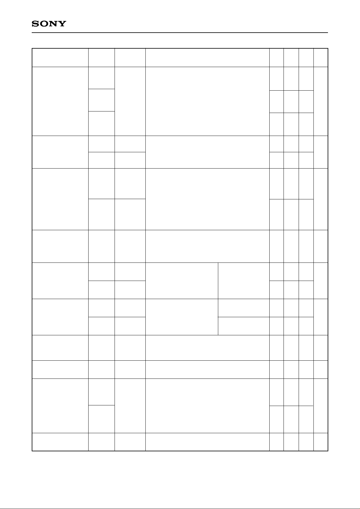
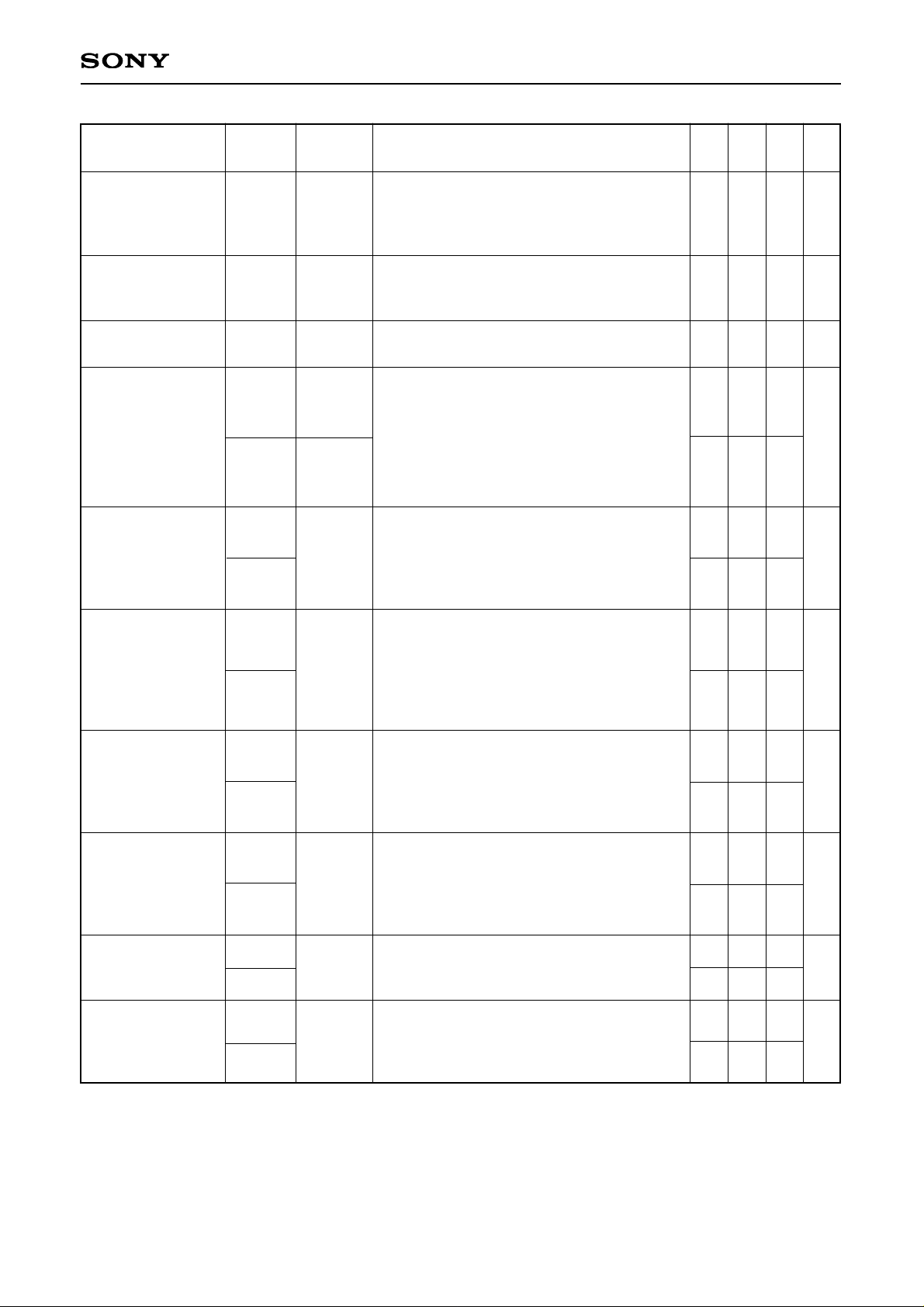
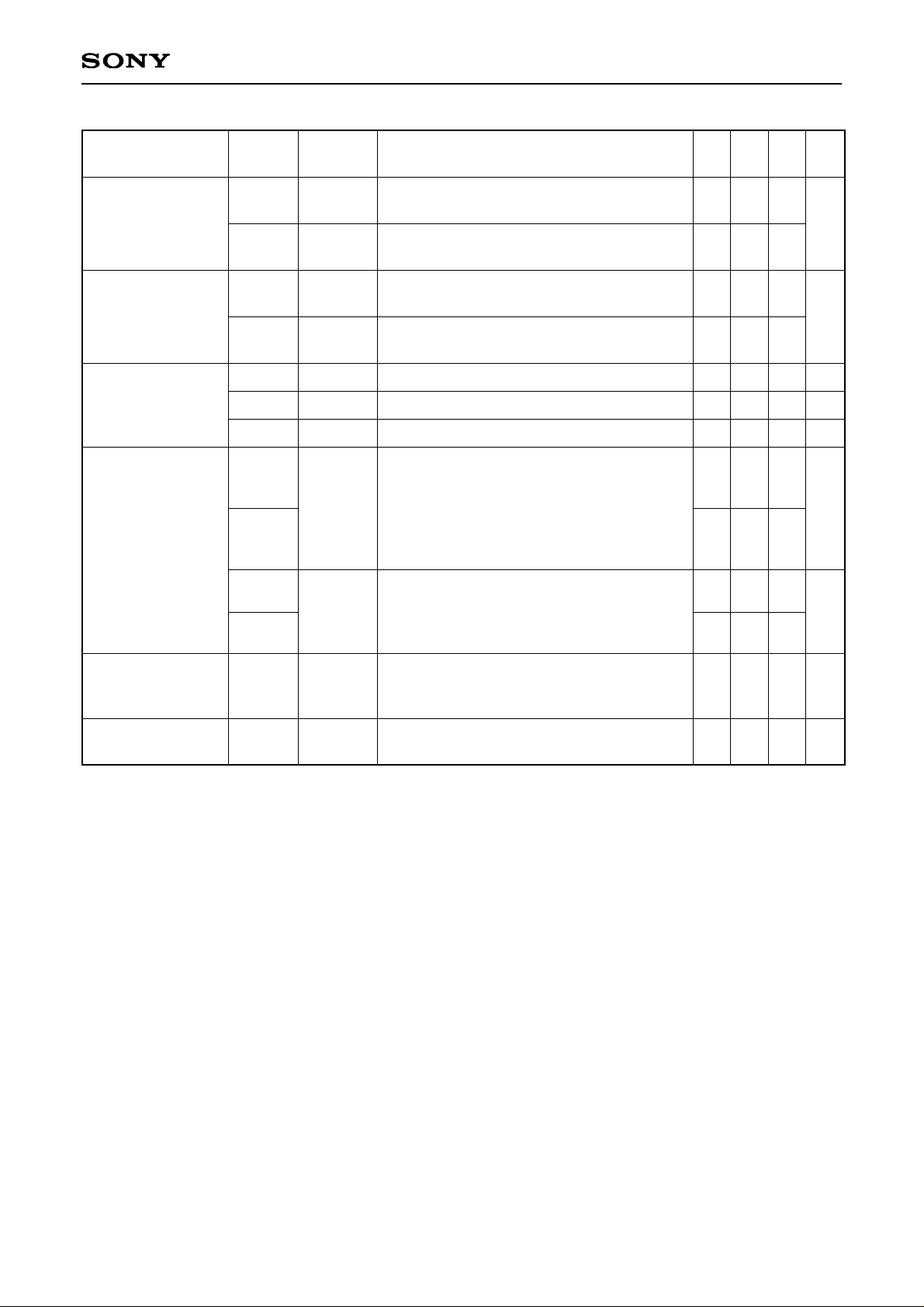
Unless otherwise specified, Settings 1 and 2, the serial data initial settings, and the following setting conditions
are required.
Ta = 25°C, VCC1 = 3.0V, VCC2 = VCC3 = 12V, GND1/2/3 = 0V, VSS = 0V, SW2 = ON, SW4 = ON,
SW32/34/36 = OFF, no video input, SG1 input to TP5
Note: Serial data values in the table are HEX notation.
Item Symbol
Serial data
setting (HEX)
Measurement conditions Min. Typ. Max. Unit
Maximum gain
between input and
output
Y/color difference
Maximum gain
between input and
output
RGB
Amount of contrast
attenuation
Inverted and
non-inverted gain
difference
Gain difference
between R, G and
B
Sub-contrast
variable amount
Sub-bright
variable amount
Black limiter
variable amount
GMAX
GRGBMAX
Gcon
∆GINV
∆GRGB1
∆GRGB2
∆GSC1
∆GSC2
∆VSB1
∆VSB2
VBL1
VBL2
CONT FFh
CONT FFh
MODE 00h
CONT 00h
CONT 2Fh
CONT 2Fh
MODE 00h
CONT 2Fh
SUB-CONT
00h
SUB-CONT
FFh
SUB-BRT
R, B 00h
SUB-BRT
R, B FFh
BLK-LIM
00h
BLK-LIM
1Fh
29
26
25
2.0
0.8
±1.6
±4.7
32
29
30
–5.5
2.7
–1.5
1.2
±2.1
±5.1
34
31
±0.3
0.6
0.6
–4.5
–1.0
±2.7
±5.4
dB
dB
dB
dB
dB
dB
V
V
Page 15
Set CONT = FFh, input SG2 (0.35Vp-p) to
TP71, measure the inverted and non-inverted
white limit level when WHITE-LIM = 00h and
03h, and assume the difference from the
output DC voltage as VWL1 and VWL2,
respectively.
Measure the non-inverted black level at
TP32, TP34 and TP36, and obtain the
maximum and minimum difference between
these values.
Measure the output DC level (average
voltage) at TP32, TP34, TP36 and TP39.
Measure the output average voltage
difference at TP32, TP34 and TP39 relative
to the output average voltage at TP36.
Measure the inverted and non-inverted black
level when PSIG-BRT = 01h and 7Fh and
assume the difference from the average DC
voltage Vc as VPB1 and VPB2, respectively.
Measure the inverted and non-inverted black
level at TP36 when U-BRT = 00h and 7Ah
and assume the difference from the average
voltage as ∆UB1 and ∆UB2, respectively.
Set BLK-LIM = 00h and measure the
difference between the inverted and noninverted black level at TP36 and TP39.
Set U-BRT = 23h, CONT = 80h, COLOR =
40h, and assume the amplitude at TP32
when SG4 (56mVp-p) is input to TP72 as V1.
Similarly, assume the amplitude at TP34
when SG4 (100mVp-p) is input to TP70 as V2.
θ = tan – 1 (V1/V2). Assume the θ when HUE
= 00h, 80h and FFh as θa, θb and θc,
respectively.
θ1 = θa – θb, θ2 = θc – θb
Set CONT = 2Fh, input SG3 to TP71, and
measure the TP36 amplitude at f0 relative to
the TP36 amplitude at 100kHz when PIC-G
= 01h and 1Fh. f0 at PIC-f0 = 00h, 01h, 02h
and 03h is 2MHz, 2.2MHz, 2.6MHz and
2.9MHz, respectively.
Input SG4 (50mVp-p) to TP70 and TP72,
and assume the output amplitude at TP32
and TP34 when COLOR = 00h, 80h and FFh
as V1, V2 and V3, respectively.
GC1 = 20 log (V1/V2)
GC2 = 20 log (V3/V2)
– 15 –
CXA3268AR
Item Symbol
Serial data
setting (HEX)
Measurement conditions
RGB and PSIG
output DC voltage
DC voltage
difference between
RGB and PSIG
PSIG-BRT
variable amount
USER-BRT
variable amount
Level difference
between PSIG-BLK
and BLK-LIM
Hue
variable amount
Picture
variable amount
Color
variable amount
Vc
∆Vc
VPB1
VPB2
∆UB1
∆UB2
∆VBB
θ1
θ2
GP1
GP2
GC1
GC2
PSIG-BRT
01h
PSIG-BRT
7Fh
U-BRT
00h
U-BRT
7Ah
SLWD
1
HUE 00h
HUE FFh
PIC-G
01h
PIC-G
1Fh
COLOR
00h
COLOR
FFh
5.8
±4.2
±4.5
–20
20
–1.5
10
5.0
6.0
±0.8
±4.9
–25
25
0
12
–30
6.0
6.2
±200
±0.7
±1.5
350
1.5
–20
V
mV
V
V
mV
deg
deg
dB
dB
VWL1
VWL2
∆VB
WHITE-LIM
00h
WHITE-LIM
03h
±1.2
±0.6
±0.6 ±0
300
V
mV
White limiter
variable amount
±1.2 ±1.8
Min. Typ. Max. Unit
Black level
difference between
R, G and B
Page 16
Set U-BRT = 30h, CONT = DFh, input SG7
(13.5MHz) to TP70, TP71 and TP72, and
measure the amount by which the output is
attenuated when FILTER = 01h relative to
FILTER = 00h. Similarly, input SG7 (14.5MHz)
to TP70, TP71 and TP72, and measure the
amount by which the output is attenuated
when FILTER = 02h relative to FILTER = 00h.
Set SW32, SW34 and SW36 = ON, input SG3
to TP70, TP71 and TP72, and measure the
frequency which results in –3dB relative to the
TP32, TP34 and TP36 amplitude at 100kHz.
Measure the REF pin
output voltage when
REF = 00h and 07h.
Measure the DA output
voltage when DA = 00h
and 07h.
Measure under the measurement conditions
for each adjustment range.
Measure under the measurement conditions
for each adjustment range.
Input SG2 (0.35mVp-p) to TP71 and measure
the amplitude at TP32, TP34 and TP36.
Assume the output amplitude when GAMMA1
= FFh as V1, when GAMMA1 = 3Fh as V2,
and when GAMMA1 = GAMMA2 = 3Fh as V3.
∆γ1 = 20 log (V1/V2)
∆γ2 = 20 log (V3/V2)
Input SG6 to TP69 and measure the output
amplitude at TP2.
– 16 –
CXA3268AR
Item Symbol
Serial data
setting (HEX)
Measurement conditions
Trap
characteristics
Frequency
response
REF adjustment
range
DA adjustment
range
Internal DAC
differential
non-linearity error
Internal DAC
non-linearity error
Gamma
characteristics
H FIL gain
fo1
fo2
f RGB
VREF1
VREF2
VDA1
VDA2
SDL
SL
∆γ1
∆γ2
Ghfil
MODE 00h
MODE 00h
MODE 00h
REF 00h
REF 07h
DA 00h
DA 07h
CONT 41h
–20
–20
5.5
1.20
1.90
2.7
–1.5
–2.0
12
12
15.0
–27
–27
1.35
2.05
14
14
17.0
1.50
2.20
0.3
1.5
2.0
16
16
dB
MHz
V
V
LSB
LSB
dB
dB
Output current
1.5mA, sink only
Output current
1.0mA
Output current
–1.0mA
Assume the TP34 output when SG4 (0.1Vp-p)
is input to TP72 as RR, the TP32 amplitude
when SG4 (0.1Vp-p) is input to TP70 as BB,
the TP34 amplitude when SG5 (0.1Vp-p) is
input to TP72 as RG, and the TP32 amplitude
when SG5 (0.1Vp-p) is input to TP70 as BG.
B-Y/R-Y = RR/BB,
G-Y/R-Y = RG/RR,
G-Y/B-Y = BG/BB
Input SG3 to TP71 and measure the
frequency which results in –3dB relative to
the TP36 amplitude at 100kHz when LPF =
01h and 07h.
B-Y/
R-Y
G-Y/
R-Y
G-Y/
B-Y
fc1
fc2
CONT 63h
COLOR
6Fh
LPF 01h
MODE 00h
LPF 07h
MODE 00h
0.85
0.41
0.15
5.0
1.00
0.51
0.19
2.0
6.4
1.15
0.61
0.23
2.5
MHz
Matrix amplitude
ratio
LPF characteristics
Min. Typ. Max. Unit
Page 17
Input SG4 to TP57, TP58 and TP59,
gradually raise the high level from 0V, and
assume the high level voltage at which the
output level goes to BLK-LIM level as
Vth1OSD, and the high level voltage at
which the output level goes to WHITE-LIM
level as Vth2OSD.
Set SW32, SW34 and SW36 = ON,
input SG4 (0.35Vp-p) to TP71, and measure
the propagation delay time of the noninverted output rise and fall at TP32, TP34
and TP36 from TP71.
Set SW32, SW34 and SW36 = ON,
input SG4 (0.35Vp-p) to TP70, TP71 and
TP72, and measure the propagation delay
time of the non-inverted output rise and fall
at TP32, TP34 and TP36 from TP70, TP71
and TP72.
Set SW32, SW34 and SW36 = ON,
input SG4 (0.35Vp-p) to TP71, and measure
the propagation delay time of the noninverted output rise and fall at TP32, TP34
and TP36 from TP71.
Set SW32, SW34 and SW36 = ON,
input SG4 (3Vp-p) to TP57, TP58 and TP59,
and measure the propagation delay time of
the non-inverted rise and fall at TP70, TP71
and TP72 from TP57, TP58 and TP59.
Input SG6 to TP69 and measure the
propagation delay time of the rise and fall at
TP2 from TP69.
Set SW2 = OFF, input SG8 to TP3, and
measure the propagation delay time of the
rise and fall at TP4 from TP3.
Measure the COM output DC voltage when
COM-DC = 00h and FFh, and measure the
difference from the COM output DC voltage
when COM-DC = 80h.
Gradually increase the SYNC IN outflow
current and measure the current at which
SYNC OUT switches to high.
Measure the SYNC OUT pin voltage during
SYNC IN no input.
– 17 –
CXA3268AR
Item Symbol
Serial data
setting (HEX)
Measurement conditions
OSD threshold
value
Propagation delay
time between input
and output
Y/color difference 1
Propagation delay
time between input
and output
RGB input
Propagation delay
time between input
and output
Y/color difference 2
Propagation delay
time between OSD
input and output
Propagation delay
time between H FIL
and FIL OUT
Propagation delay
time between
SYNC IN and
SYNC OUT
Vth1
OSD
Vth2
OSD
tLH1
tHL1
tLH2
tHL2
tLH3
tHL3
tLH4
tHL4
tLH7
tHL7
tLH8
tHL8
MODE
00h
PIC-G
01h
0.8
1.8
70
80
70
60
270
270
90
170
500
100
140
40
1.0
2.0
120
130
110
110
330
330
130
210
700
300
200
100
1.2
2.2
170
180
160
160
390
390
170
250
900
500
260
160
V
ns
ns
ns
ns
ns
ns
COMMON control
range
SYNC IN
sensitivity current
SYNC OUT on
voltage
COMDC
I SYNC
VOsync
±1.0
20
±1.3
31
0.2 0.4
V
µA
V
Min. Typ. Max. Unit
Page 18
– 18 –
CXA3268AR
Data setup time
Data hold time
Minimum pulse
width
Output transition
time
Cross-point time
difference
HCK duty
ts0
ts1
th0
th1
tw1L
tw1H
tw2
∆T
DTYHC
SEN setup time, activated by the rising edge
of SCK. (See Fig. 4.)
SDAT setup time, activated by the rising
edge of SCK. (See Fig. 4.)
SEN hold time, activated by the rising edge
of SCK. (See Fig. 4.)
SDAT hold time, activated by the rising edge
of SCK. (See Fig. 4.)
SCK pulse width. (See Fig. 4.)
SCK pulse width. (See Fig. 4.)
SEN pulse width. (See Fig. 4.)
Measure the transition time of each output.
30pF load: RPD, VDO, HDO and POF
output pins
40pF load: EN and HST output pins
120pF load: HCK1 and HCK2 output pins
(See Fig. 2.)
Measure the transition time of each output.
40pF load: DWN, WIDE, VCK, VST and
RGT output pins
(See Fig. 2.)
Measure HCK1/HCK2.
120pF load
(See Fig. 3.)
Measure the HCK1/HCK2 duty.
120pF load
501053
ns
ns
ns
ns
µs
ns
ns
ns
%
150
150
150
150
210
210
1
47
Item Symbol
Serial data
setting (HEX)
Measurement conditions
30
tTLH
30
50
50
tTHL
tTLH
tTHL
Min.
Typ. Max. Unit
Page 19
– 19 –
CXA3268AR
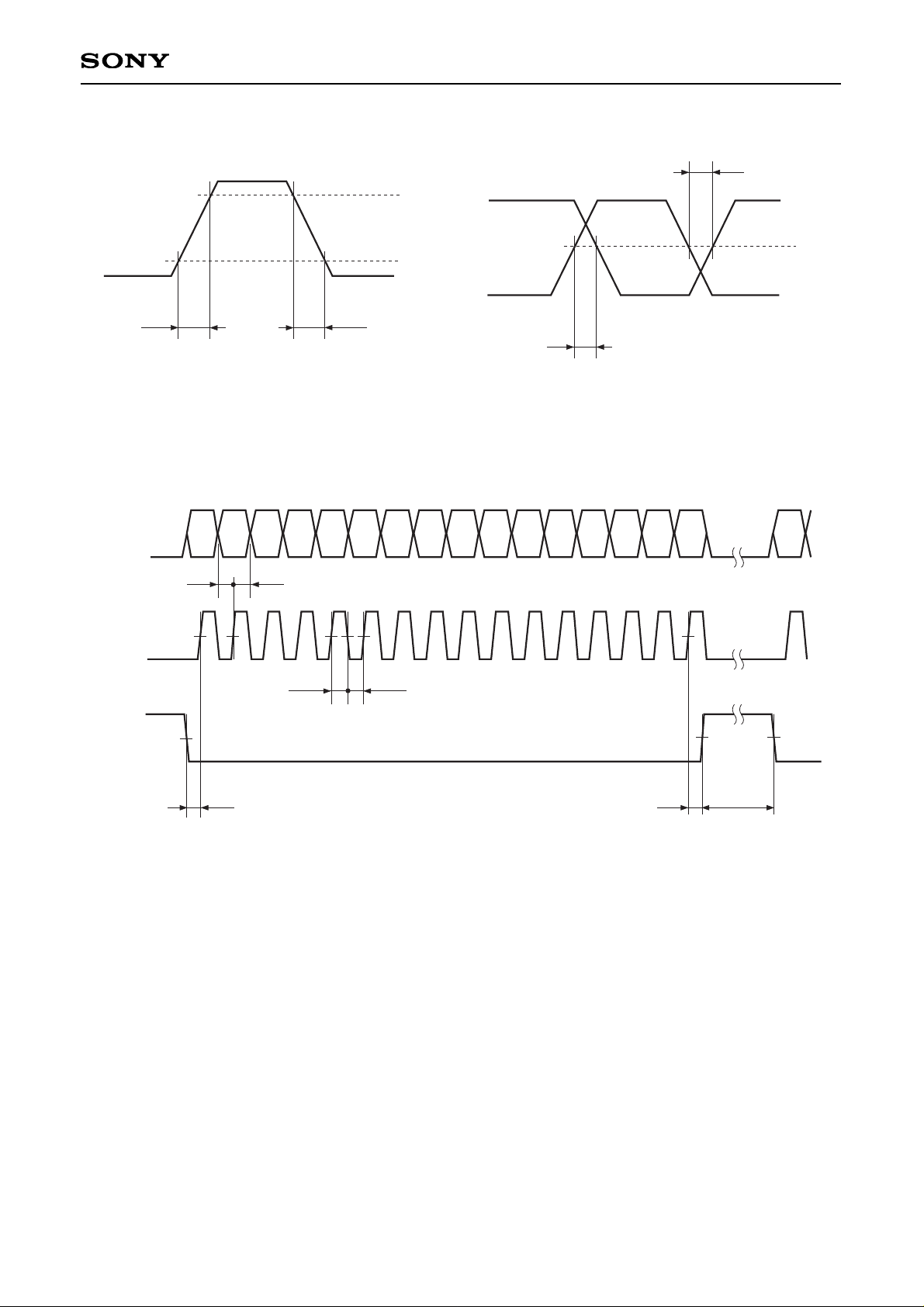
Electrical Characteristic Measurement Method Diagrams
tTLH
90%
10%
tTHL
50%
∆T
∆T
Fig. 2. Output transition time
measurement conditions
Fig. 3. Cross-point time difference
measurement conditions
Fig. 4. Serial transfer block measurement conditions
D15SDTA
SCK
SEN
ts1 th1
tw1H tw1L
th0 tw2ts0
D14 D13 D12 D11 D10 D9 D8 D7 D6 D5 D4 D3 D2 D1 D0 D15
50%
50%
Page 20

– 20 –
CXA3268AR
SG No.
SG1
SG2
SG3
SG4
SG5
Waveform
1H
3.0Vp-p
Horizontal sync signal
(CSYNC)
4.7µs
1H
Amplitude variable
Horizontal sync signal
0.1Vp-p
0.1Vp-p
1H
High level variable
0V
Horizontal sync signal
25µs 10µs
25µs
10µs
3V
Low level variable
Horizontal sync signal
Sine wave video signal; frequency and amplitude variable
Page 21

– 21 –
CXA3268AR
SG No.
SG6
Waveform
1H
50mVp-p
Horizontal sync signal
(CSYNC)
4.7µs
SG7
0.1Vp-p
1H
Sine wave video signal
SG8
1H
0.15Vp-p
Horizontal sync signal
(CSYNC)
4.7ns
Page 22
– 22 –
CXA3268AR
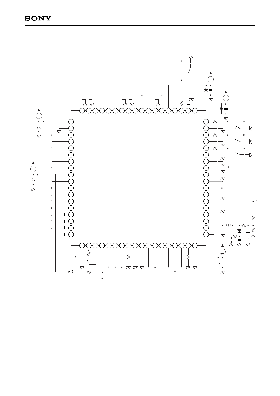
Electrical Characteristics Measurement Circuit
Vss
FIL OUT
SYNC IN
SYNC OUT
CSYNC/HD
G OUT
G DC DET
R OUT
R DC DET
B OUT
B DC DET
SIG.C
GND2
TST2
HDO
XCLR
VDO
RPD
Vss
CKI
CKO
V
DD
VDD
VDD
TST11
OSD B
OSD R
OSD G
NC
HCK1
HCK2
Vcc1
HST
EN
VCK
VST
RGT
FIL IN
B/B-Y
G/Y
R/R-Y
Vss
Vss
TST10
TST9
TST8
TST7
TST6
TST5
NC
POF
TST4
GND3
COM
Vcc3
TST3
PSIG OUT
PSIG DC DET
Vcc2
+3V
+12V
V22 0.01µ
3.3µ 1000p
6800p
33k
1k
TP24
10k
3.3µ
0.01µ47µ
+12V
1µ47µ
+12V
400P
SW39
TP39
1µ47µ
1µ
47µ
30p
10k
∗
2
∗1
Resistance value tolerance: ±2%, temperature coefficient: ±200ppm or less
Locate this resistor as close to the IC pin as possible to reduce the effects of external signals.
∗2
Varicap diode: 1T369 (SONY)
0.1µ
0.01µ
0.1µ
0.1µ
1µ
SW2
TP6 TP7
TP14
TP15
TP16
TP3
1k
SW4
TP2
0.1µ
0.1µ
10
10
+3V
0.01µ47µ
TP57
TP69
TP70
TP71
TP72
TP58
TP42
TP30
TP59
1µ
0.01µ
0.01µ
0.01µ
37
38
3940
41
42434445464748495051525354
55
56
57
58
59
60
61
62
63
64
65
66
67
68
69
70
71
72
1
2
3 4
DA OUT
REF
F ADJ
GND1
VD
DWN
WIDE
TST1
SCK
SEN
SDAT
R INJECT
V
SS
∗1
15k33k
TP5
TP4
6
7
8 9 11 12 13 14
15
16 17 18
19
20
21
22
23
24
25
26
27
28
29
30
31
33
35
36
A
A
A
A
A
300P
SW36
TP36
10
300P
SW34
TP34
10
300P
SW32
TP32
34
32
5 10
TP45
TP27
TP26
∗
1
TP11
TP12
TP68
TP67
TP66
TP65
TP64
TP61
TP62
Page 23

– 23 –
CXA3268AR
Description of Operation
1) RGB and Y/color difference signal processing block
Signal processing is comprised of picture, hue, matrix, LPF/trap, contrast, OSD, sample-and-hold, γ correction,
bright, sub-bright, sub-contrast and output circuits
• Input signal mode switching
The input mode (RGB input, Y/color difference input) can be switched by the serial communication settings.
(During internal sync separation signal input)
During RGB input: The G signal is input to Pins 71 and 69, the B signal to Pin 70, and the R-Y signal to
Pin 72.
During Y/color difference input: The Y signal is input to Pins 71 and 69, the B-Y signal to Pin 70, and the
R-Y signal to Pin 72.
(During external sync signal input)
During RGB input: The G signal is input to Pin 71, the B signal to Pin 70, the R signal to Pin 72,
CSYNC/HD to Pin 5, and VD to Pin 10.
During Y/color difference input: The Y signal is input to Pin 71, the B-Y signal to Pin 70, the R-Y signal to
Pin 72, CSYNC/HD to Pin 5, and VD to Pin 10.
• NTSC/PAL switching
The input system (NTSC/PAL) can be switched by the serial communication settings.
• Picture circuit
This performs aperture correction for the Y signal. The center frequency to be corrected and the correction
amount are controlled by serial communication. In addition, when not using the picture circuit, it can be turned
off by serial communication.
• Hue circuit
This is the hue adjustment circuit for the color difference signal. It is controlled by serial communication.
• Matrix circuit
This circuit converts Y, R-Y and B-Y signals into RGB signals.
• LPF circuit
This is the band limitation filter for the RGB signal. It is used to eliminate the noise component generated at
the front end of this IC. The cut-off frequency can be controlled by serial communication. In addition, when
not using the LPF, it can be turned off by serial communication.
• Trap circuit
This is used to eliminate the DSP clock and RGB decoder carrier leak generated at the front end of this IC.
The center frequency can be switched between 13.5MHz and 14.3MHz by serial communication. In addition,
when not using the trap, it can be turned off by serial communication.
• Contrast adjustment circuit
This adjusts the white-black amplitude to set the input RGB signal to the appropriate output level.
• OSD
This inputs the OSD pulses. There are two input threshold values: Vth1 (VCC1 × 1/3) and Vth2 (VCC1 × 2/3).
When an input exceeds Vth1, the corresponding output falls to the level specified by BLACK-LIMITE. When
an input exceeds Vth2, the corresponding output rises to the level specified by WHITE-LIMITER. Also, when
one of the RGB inputs exceeds Vth1, any signal outputs not exceeding Vth1 also fall to the level specified by
BLACK-LIMITER.
Page 24
– 24 –
CXA3268AR
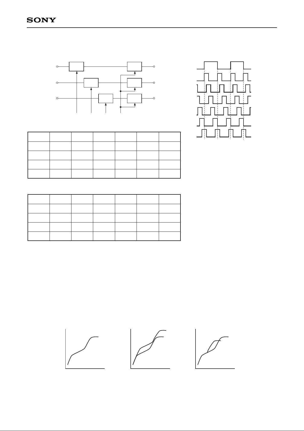
• Sample-and-hold circuit
This circuit performs time axis correction for the RGB output signals in order to support the RGB simultaneous
sampling systems of LCD panels.
The sample-and-hold circuit performs sample-and-hold by receiving the SH1 to SH4 pulses from the TG
block. Since LCD panels perform color coding using an RGB delta arrangement, each horizontal line must be
compensated by 1.5 dots. This relationship is reversed during right/left inversion. This compensation and
other timing is also generated by the digital block. The sample-and-hold timing changes according to the
phase relationship with the HCK pulse, so the timing should be set to the SHS1, 2 or 6 position in
accordance with the actual board.
• γ correction
In order to support the characteristics of LCD panels, the I/O characteristics are as shown in Fig. 1. The γ1
gain transition point A voltage changes as shown in Fig. 2 by adjusting the serial bus register γ1, and the γ2
gain transition point B voltage changes as shown in Fig. 3 by adjusting γ2.
Output
Input
B
B"
A'
A
Output
Input
B
B'
A
Output
Input
Fig. 1 Fig. 2 Fig. 3
B
A
SH1: R signal SH pulse
SH2: G signal SH pulse
SH3: B signal SH pulse
SH4: RGB signal SH pulse
SHS1,2,3,4,5,6: Serial data settings
SH1
SH2
SH3
SH4
SHS1
B
A
Through
C
SHS2
A'
C'
Through
B'
SHS3
A
C
Through
B
SHS4
C'
B'
Through
A'
SHS5
C
B
Through
A
SHS6
B'
A'
Through
C'
RGT = L (right/left inversion)
SH1
SH2
SH3
SH4
SHS1
B
Through
A
C
SHS2
A'
Through
C'
B'
SHS3
A
Through
C
B
SHS4
C'
Through
B'
A'
SHS5
C
Through
B
A
SHS6
B'
Through
A'
C'
RGT = H (normal)
HCK1
A
A'
B'
B
C
C'
S/H1 S/H4
S/H2 S/H4
S/H3
SH3 SH4SH2SH1
S/H4
R
G
B
R
G
B
Page 25
– 25 –
CXA3268AR
Set by BLACK-LIMITER
BLACK-LIMITER
SIG.C
BLACK-LIMITER
BLACK-LIMITER
SIG.C
WHITE-LIMITER
WHITE-LIMITER
BLACK-LIMITER
Set by BLACK-LIMITER
Set by PSIG-BRIGHT
RGB IN
1H inverted signal
(internal)
16:9 display signal
(internal)
PSIG OUT
RGB OUT
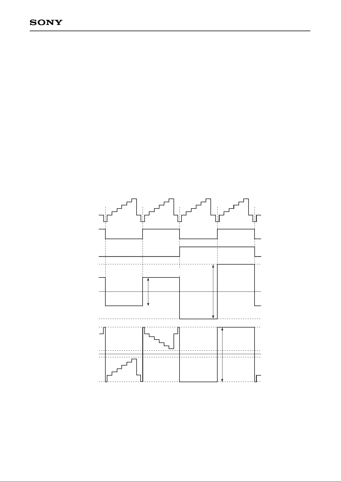
• Bright circuit
This is used to adjust the black-black amplitude of polarity-inverted RGB output signals. It is not interlinked
with the γ transition points.
• White balance adjustment circuit
This is used to adjust the white balance. The black level is adjusted by SUB-BRIGHT, and the black-white
amplitude is adjusted by SUB-CONTRAST.
• Output circuit
RGB output (Pins 70, 71, and 72) signals are inverted each horizontal line by the FRP pulse (internal pulse)
supplied from the TG block as shown in the figure below. Feedback is applied so that the center voltage
(SIG.C) of the output signal matches the reference voltage (VCC2 + GND2)/2 (or the voltage input to SIG.C
(Pin 30)). In addition, the white level output is clipped at the limiter operation point that is set by the serial
communication WHITE-LIMITER, and the black level output is clipped at the limiter operation point that is set
by the serial communication BLACK-LIMITER.
The output PSIG signal level is normally adjusted by PSIG-BRIGHT, but during 16:9 display the level is
specified by BLACK-LIMITER during V blanking. In addition, the RGB output also simultaneously goes to
BLACK-LIMITER level output.
Page 26

– 26 –
CXA3268AR
2) Common voltage generation circuit block
The common voltage circuit generates and supplies the common pad voltage to the LCD panel. The voltage
is offset by serial communication using the SIG.C voltage as the reference and then output.
3) DAC output circuit
There are two DAC output circuit systems. The DA OUT output circuit outputs DC 3.0V at equal divisions.
The REF output circuit generates and supplies the REF voltage for the panel level shifter circuit to the LCD
panel. Both circuits are controlled by serial communication.
4) Sync system
• H FIL
This amplifies the sync signal of the input video signal and eliminates the noise with an internal LPF. The sync
signal is clamped at the input, so be sure to input via a capacitor.
• SYNC SEP
This inputs the FIL OUT (Pin 2) output and performs sync separation. The signal is output from SYNC OUT
(Pin 4) as a positive polarity pulse.
5) Power saving circuit (PS circuit)
A power saving system can be realized together with the LCD panel by independently controlling (serial
communication) the operation of each output block. This system is also effective for improving picture
quality during power-on/off.
The serial data PS0, PS1, PS2, PS4 and SYNC GEN must be set in order to use this IC. For details of
the setting methods, see the "Description of Serial Control Operation" and "Power Supply and Power
Saving Sequence" items.
Page 27
– 27 –
CXA3268AR
6) TG block
• PLL and AFC circuits
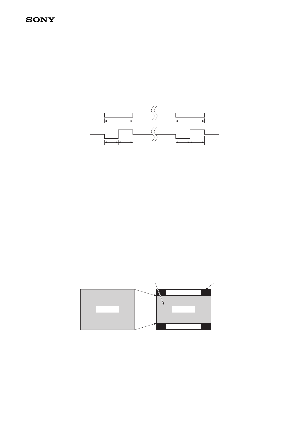
A PLL circuit can be comprised by connecting a PLL circuit phase comparator and frequency division counter
and external VCO and LPF circuits.
The PLL error detection signal is generated using the phase comparison output of the entire bottom of the
horizontal sync signal and the internal frequency division counter as the RPD output. RPD output is
converted to DC error voltage with the lag-lead filter, and then it changes the capacitance of the varicap
diode to stabilize the oscillation frequency.
The PLL of this system is adjusted by setting the reverse bias voltage of the varicap diode so that the point at
which RPD changes is at the center of the horizontal sync signal window as shown in the figure below.
Horizontal sync signal
RPD (Pin 24)
WS
WL WH WL WH WL = WH
WS
• H-Position
This adjusts the horizontal display position. Set this function so that the picture center matches the center of
the LCD panel.
• Right/left (RGT) and/or up/down inversion (DWN)
The video display direction can be switched. The horizontal direction can be switched between right scan and
left scan, and the vertical direction between down scan and up scan. Set the display direction in accordance
with the LCD panel mounting position.
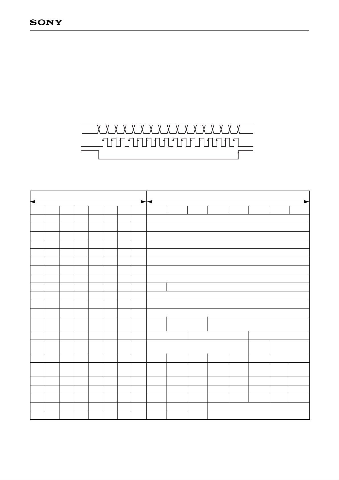
• Wide mode
16:9 quasi-WIDE display can be achieved by converting the aspect ratio through pulse elimination processing.
During wide mode, vertical pulse elimination scanning is performed for both NTSC and PAL display and the
video signal is compressed to achieve a 16:9 aspect ratio. In addition, in areas outside the display area, the
black level set by BLACK-LIMITER (serial communication data) is wide-masked as the black signal within the
limited vertical blanking period.
This function achieves a quasi-display by simply pulse eliminating the video signal, so some video information
is lost.
Display area Display area
Black display area
Pulse elimination display
Black display
Black display area
16:9 display4:3 display
172 LINES228 LINES
28 LINES
28 LINES
• AC driving of LCD panels during no signal
The output signal runs freely so that the LCD panel is AC driven even when there is no sync signal from the
FIL IN (Pin 69) pin or from the CSYNC/HD (Pin 5) and VD (Pin 10) pins. During this time, the sync separation
circuit stops and the auxiliary counter is used to generate the free running output pulses after detecting that
there is no vertical sync signal for approximately 3 fields (no signal state).
Page 28
PSIG-BRIGHT
– 28 –
CXA3268AR
Description of Serial Control Operation
1) Control method
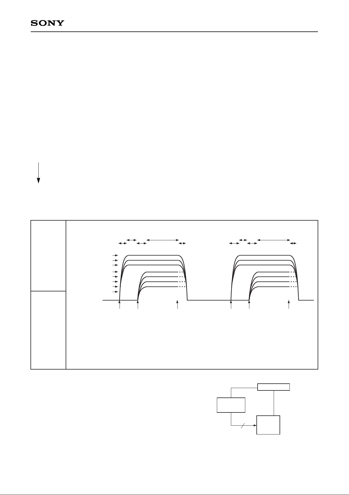
Control data consists of 16 bits of data which is loaded one bit at a time at the rising edge of SCK. This loading
operation starts from the falling edge of SEN and is completed at the next rising edge.
Digital block control data is established by the vertical sync signal, so if data is transferred multiple times for
the same item, the data immediately before the vertical sync signal is valid. Analog (electronic attenuator)
block control data becomes valid each time the SEN signal is input.
In addition, if 16 bits of more of SCK are not input while SEN is low, the transferred data is not loaded to the
inside of the IC and is ignored. If 16 bits or more of SCK are input, the 16 bits of data before the rising edge of
the SEN pulse are valid data.
SDAT A7 A6 A5 A4 A3 A2 A1 A0 D7 D6 D5 D4 D3 D2 D1 D0
SCK
SEN
D: DATAA: ADDRESS
Serial transfer timing
2) Serial data map
The serial data map is as follows. Values inside parentheses are the default values.
Note) If there is the possibility that data may be set at other than the above-noted addresses, set these data to "0".
MSB ADDRESS LSB MSB DATA LSB
D15 D14 D13 D12 D11 D10 D9 D8 D7 D6 D5 D4 D3 D2 D1 D0
0
0
0
0
0
0
0
0
0
0
0
0
0
0
0
0
0
0
0
0
0
0
0
0
0
0
0
0
0
0
0
0
0
0
0
0
0
0
0
0
0
0
0
0
0
0
0
0
0
0
0
0
0
0
0
0
0
0
0
0
0
1
1
1
1
1
0
0
0
0
0
0
0
0
0
0
0
0
0
0
0
0
1
0
0
0
0
0
0
0
0
0
0
0
0
0
1
1
1
1
1
1
1
1
0
0
0
0
0
0
0
0
0
0
1
1
1
1
0
0
0
0
1
1
1
1
0
0
0
0
0
1
0
0
1
1
0
0
1
1
0
0
1
1
0
0
1
1
0
0
0
1
1
0
0
1
0
1
0
1
0
1
0
1
0
1
0
1
0
1
0
0
1
0
1
0
USER-BRIGHT
SUB-BRIGHT R
SUB-BRIGHT B
CONTRAST
SUB-CONTRAST R
SUB-CONTRAST B
γ-2
γ-1
(0)
COM-DC
COLOR
HUE
(10000000/LSB)
(10000000/LSB)
(10000000/LSB)
(10000000/LSB)
(10000000/LSB)
(10000000/LSB)
(00000000/LSB)
(00000000/LSB)
(1000000/LSB)
(10000000/LSB)
(10000000/LSB)
(10000000/LSB)
WHITE-LIMITER
(00/LSB)
BLACK-LIMITER (10000/LSB)
LPF (000/LSB)
REF (011/LSB)
FILTER (00/LSB)
PICTURE-F0
(00/LSB)
PICTURE-GAIN (00000/LSB)
(0) (0) (0) (0)
MODE (0)
DA (000/LSB)
(0)
SLSYP (0)
(0)
(0)
(0)
(0)
(0)
SLEXVD (0)
SLFL (0)
(0)
(0)
(0)
SYNC GEN
(1)
SLDWN (0)
SLFR (0)
SLTST4 (0)
(0)
(0)
PS 4
(1)
SLRGT (0)
SL4096 (0)
SLTST3 (0)
(0)
SLSH2 (0)
SLCLP2 (0)
SLSH0 (0)
PS 2
(1)
SLSH1 (0)
SLCLP1 (0)
SLTST2 (0)
PS 1
(1)
SLWD (0)
SLVDP (0)
SLTST1 (0)
PS 0
(1)
SLPL (0)
SLHDP (0)
SLTST0 (0)
H-POSITION (10000/LSB)
HD-POSITION (00000/LSB)
(0)
(0)
Page 29

– 29 –
CXA3268AR
3) Description of control data
• USER-BRIGHT
This adjusts the brightness of the RGB output signals. Adjustment from LSB → MSB increases the amplitude
(black-black).
• SUB-BRIGHT R/B
This adjusts the brightness of the R and B output signals using the G output signal as the reference.
Adjustment from LSB → MSB increases the amplitude (black-black).
• CONTRAST
This adjusts the contrast of the RGB output signals. Adjustment from LSB → MSB increases the amplitude
(black-white).
• SUB-CONTRAST R/B
This adjusts the contrast of the R and B output signals using the G output signal as the reference.
Adjustment from LSB → MSB increases the amplitude (black-black).
• γ-2
This sets the white side γ point level of the RGB output signals. Adjustment from MSB → LSB lowers the γ point.
When not adjusting γ-2, set γ-2: 11111111 (LSB). Set the γ-2 point to the white side of the γ-1 point.
• γ-1
This sets the black side γ point level of the RGB output signals. Adjustment from MSB → LSB lowers the γ point.
When not adjusting γ-1, set γ-1: 11111111 (LSB). Set the γ-1 point to the black side of the γ-2 point.
• PSIG-BRIGHT
This adjusts the bright level of the PSIG output signal. Adjustment from LSB → MSB increases the amplitude
(peak to peak).
Note: Do not set PSIG-BRIGHT: 0000000 (LSB), as this setting turns off the internal PSIG circuit.
• COM-DC
This adjusts the COMMON output voltage. Adjustment from LSB → MSB increases the output voltage.
• COLOR
This adjusts the color gain during Y/color difference input. Adjustment from LSB → MSB increases the gain.
• HUE
This adjusts the phase during Y/color difference input. Adjustment from LSB → MSB advances the phase.
• WHITE-LIMITER
This adjusts the white side limiter level of the RGB output signals. See the AC Characteristics for the output
level.
• BLACK-LIMITER
This adjusts the black side limiter level of the RGB output signals. Adjustment from LSB → MSB lowers the
limiter level.
Page 30

– 30 –
CXA3268AR
• LPF
This switches the frequency response of the low-pass filter. Set the fc/–3dB frequency relative to the amplitude
100kHz reference. See the AC Characteristics for the output level.
• REF
This adjusts the REF output voltage. Adjustment from LSB → MSB raises the output voltage level. See the
AC Characteristics for the output level.
D1
0
0
1
1
0
0
1
1
D0
0
1
0
1
0
1
0
1
D2
0
0
0
0
1
1
1
1
fc (RGB input/no load/typ.)
LPF OFF
2.0MHz
2.7MHz
3.4MHz
3.9MHz
4.9MHz
5.7MHz
6.4MHz
• FILTER
This sets the trap (f0) center frequency. See the AC Characteristics for the output level.
D6
0
1
0
1
D7
0
0
1
1
Center frequency (f0)
TRAP OFF
13.5MHz
14.3MHz
—
• PICTURE-F0
This sets the picture center frequency (f0) during Y/color difference input. See the AC Characteristics for the
output level.
D0
0
1
0
1
D1
0
0
1
1
Center frequency (f0)
2.0MHz (typ.)
2.2MHz (typ.)
2.6MHz (typ.)
2.9MHz (typ.)
• PICTURE-VOLUME
This adjusts the picture gain during Y/color difference input. Adjustment from LSB → MSB raises the gain.
When not using the picture function (OFF), set PICTURE-VOLUME: 00000 (LSB).
Page 31

– 31 –
CXA3268AR
• SYNC GEN
This sync generator mode stops all output pulses other than the HDO and VDO output pulses. The PS0,
PS1, PS2 and PS4 settings have priority over the SYNC GEN setting. Normally set to "0".
D5
0
1
Mode (SYNC GEN)
Normal operation
All output pulses and corresponding output blocks other than the HDO and VDO output pulses are
stopped.
• PS0, PS1, PS2, PS4
These perform the power saving settings for each input and output block. Be sure to use these settings as
described in "Power Supply and Power Saving Sequence". The power-on default for this IC is power saving
mode, so the settings should be canceled by serial communication after power-on.
D0, 1, 2, 4
0
1
Mode (PS0, PS1, PS2, PS4)
Normal operation
The respective outputs and corresponding output blocks are stopped.
• DA
This adjusts the DA output voltage. See the AC Characteristics for the output level.
• MODE
This switches the input signal.
D3
0
1
Input signal
RGB input
Y/color difference input
Page 32
– 32 –
CXA3268AR
Fig. 2. System block diagram
Power Supply and Power Saving Sequence
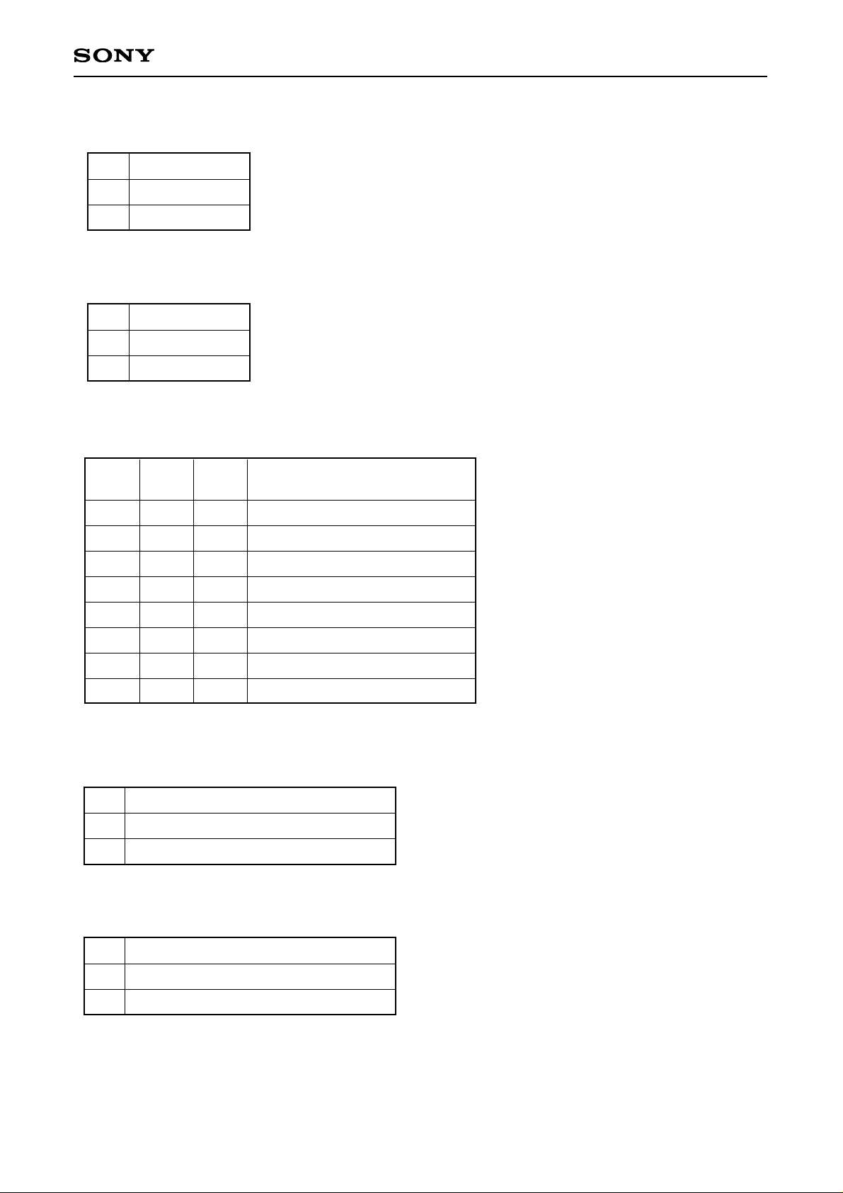
When using this IC, the power supply sequences described below must be followed during power-on/off to
ensure reliability as a LCD driving system. Thoroughly study the function specifications of each control method
(1), (2) and (3) before use.
Control timing (1)
Use this timing when not using the power saving (PS) function regardless of picture quality during poweron/off.
Control timing (2)
Use this timing when using the power saving (PS) function regardless of picture quality during power-on/off.
Note that in this case an external switch is necessary.
Control timing (3)
Use this timing when using the power saving (PS) function and placing priority on picture quality during
power-on/off. Note that in this case an external switch is necessary.
Control timing (1)
(1) IC power-on (3V, 12V), LCD power-on (HVDD, VVDD)
(2) A settings: after the IC and LCD power supplies have risen
(3) IC power-off (3V, 12V), LCD power-off (HVDD, VVDD): optional
The LCD power supply (HVDD, VVDD) rise timing should adequately satisfy the panel specifications.
Serial data settings other than PS should be made during the control period from the rise of the IC 3V
power supply to (2).
∗1
During IC power-on (default status), the PS mode is activated
(the PS0, PS1, PS2, PS4 and SYNC GEN data are all set to "1").
Therefore, the PS settings should be canceled via serial
communication in accordance with the sequence specifications.
∗2
When inputting the sync signal from an external source, set serial
data PS4 = 1.
LCD power supply
IC 12V
IC 3V
SYNC GEN circuit
PS4 circuit
PS2 circuit
PS1 circuit
PS0 circuit
Default LCD display
Fig. 1
PS OFFPower-on Power-off
∗1 ∗1
∗2 ∗2
Default LCD display
PS OFFPower-on Power-off
Status
Supply voltage
&
output signal
Operation
Power-on/off
&
PS settings
(serial data)
IC power-on
LCD power-on
A
PS0 → 0
PS1 → 0
PS2 → 0
PS4 → 0 (1)
SYNC GEN
→ 0
IC power-on
LCD power-on
IC power-off
LCD power-off
IC power-off
LCD power-off
A
PS0 → 0
PS1 → 0
PS2 → 0
PS4 → 0 (1)
SYNC GEN
→ 0
VCC/VDD
CXA3268AR
LCD
Signal
HV
DD/
VV
DD
Power supply
Page 33

– 33 –
CXA3268AR
Control timing (2)
(1) IC power-on (3V, 12V), LCD power-on (HVDD, VVDD)
(2) A settings: after the IC and LCD power supplies have risen
(3) B settings: optional
(4) IC power-off (3V, 12V), LCD power-off (HVDD, VVDD): optional
It is possible to skip from step (2) to step (4) without making the B settings (dotted lines in the figure).
The LCD power supply (HVDD, VVDD) rise timing should adequately satisfy the panel specifications.
Serial data settings other than PS should be made during the control period from the rise of the IC 3V
power supply to (2).
∗1
During IC power-on (default status), the PS mode is activated
(the PS0, PS1, PS2, PS4 and SYNC GEN data are all set to "1").
Therefore, the PS settings should be canceled via serial
communication in accordance with the sequence specifications.
∗2
When inputting the sync signal from an external source, set serial
data PS4 = 1.
LCD power supply
IC 12V
IC 3V
SYNC GEN circuit
PS4 circuit
PS2 circuit
PS1 circuit
PS0 circuit
Fig. 1
PS ON
∗1
∗2 ∗2
PSPS (Default) LCD display LCD displayPS
PS OFF
PS OFF Power-offPower-on PS ON
IC power-on
LCD power-on
A
PS0 → 0
PS1 → 0
PS2 → 0
PS4 → 0 (1)
SYNC GEN
→ 0
SYNC GEN
→ 1
IC power-off
LCD power-off
A
PS0 → 0
PS1 → 0
PS2 → 0
PS4 → 0 (1)
B
PS0 → 1
PS1 → 1
PS2 → 1
PS4 → 1
B
PS0 → 1
PS1 → 1
PS2 → 1
PS4 → 1
SYNC GEN
→ 0
SYNC GEN
→ 1
Status
Supply voltage
&
output signal
Operation
Power-on/off
&
PS settings
(serial data)
VCC/VDD
CXA3268AR
LCD
SW
Signal
HV
DD/
VV
DD
3V output
POF pin
Power supply
Fig. 2. System block diagram
Page 34

– 34 –
CXA3268AR
Control timing (3)
(1) IC power-on (3V)
(2) IC power-on (12V), LCD power-on (HVDD, VVDD): after the IC power supply (3V) has completely risen
(3) A settings: after the IC (12V) and LCD power supplies have risen
(4) B settings: after the PLL has stabilized (stable RPD waveform) and the panel I/O power supply conditions
have been satisfied.
(5) C settings: optional
(6) D settings: after COM/CS, RGB and PSIG have fallen
(7) E settings: 100ms or more after the D settings
(8) IC power-off (12V), LCD power-off (HVDD, VVDD): after the HVDD and VVDD pin voltages have fallen
(9) IC power-off (3V): after the IC power supply (12V) has completely fallen
Serial data settings other than PS should be made during the control period from the rise of the IC 3V
power supply to (3).
The LCD power supply (HVDD, VVDD) rise timing should adequately satisfy the panel specifications.
∗1
During IC power-on (default status), the PS mode is activated
(the PS0, PS1, PS2, PS4 and SYNC GEN data are all set to "1").
Therefore, the PS settings should be canceled via serial
communication in accordance with the sequence specifications.
∗2
When inputting the sync signal from an external source, set serial
data PS4 = 1.
∗3
When raising the power supplies, first raise the IC 3V power
supply, then raise the IC 12V and LCD power supplies.
∗4
When lowering the power supplies, first lower the LCD and IC
12V power supplies, then lower the IC 3V power supply.
LCD power supply
IC 12V
IC 3V
SYNC GEN circuit
PS4 circuit
PS2 circuit
PS1 circuit
PS0 circuit
Fig. 1
PS ON
∗1 ∗3 ∗4
∗2 ∗2
PSPS (Default) LCD display LCD displayPS
PS OFF
PS OFF Power-offPower-on PS ON
IC power-on
LCD power-on
A
PS0 → 0
PS1 → 0
PS2 → 0
PS4 → 0
SYNC GEN
→ 1
B
PS0 → 0
PS1 → 0
PS2 → 0
PS4 → 0 (1)
SYNC GEN
→ 0
C
PS0 → 1
PS1 → 0
PS2 → 0
PS4 → 0 (1)
SYNC GEN
→ 0
D
PS0 → 1
PS1 → 1
PS2 → 0
PS4 → 0 (1)
SYNC GEN
→ 0
C
PS0 → 1
PS1 → 0
PS2 → 0
PS4 → 0 (1)
SYNC GEN
→ 0
D
PS0 → 1
PS1 → 1
PS2 → 0
PS4 → 0 (1)
SYNC GEN
→ 0
E
PS0 → 1
PS1 → 1
PS2 → 1
PS4 → 1
SYNC GEN
→ 1
E
PS0 → 1
PS1 → 1
PS2 → 1
PS4 → 1
SYNC GEN
→ 1
IC power-off
LCD power-off
A
PS0 → 0
PS1 → 0
PS2 → 0
PS4 → 0
SYNC GEN
→ 1
B
PS0 → 0
PS1 → 0
PS2 → 0
PS4 → 0 (1)
SYNC GEN
→ 0
Status
Supply voltage
&
output signal
Operation
Power-on/off
&
PS settings
(serial data)
VCC/VDD
CXA3268AR
LCD
SW
Signal
HV
DD/
VV
DD
3V output
POF pin
Power supply
Fig. 2. System block diagram
Page 35
– 35 –
CXA3268AR
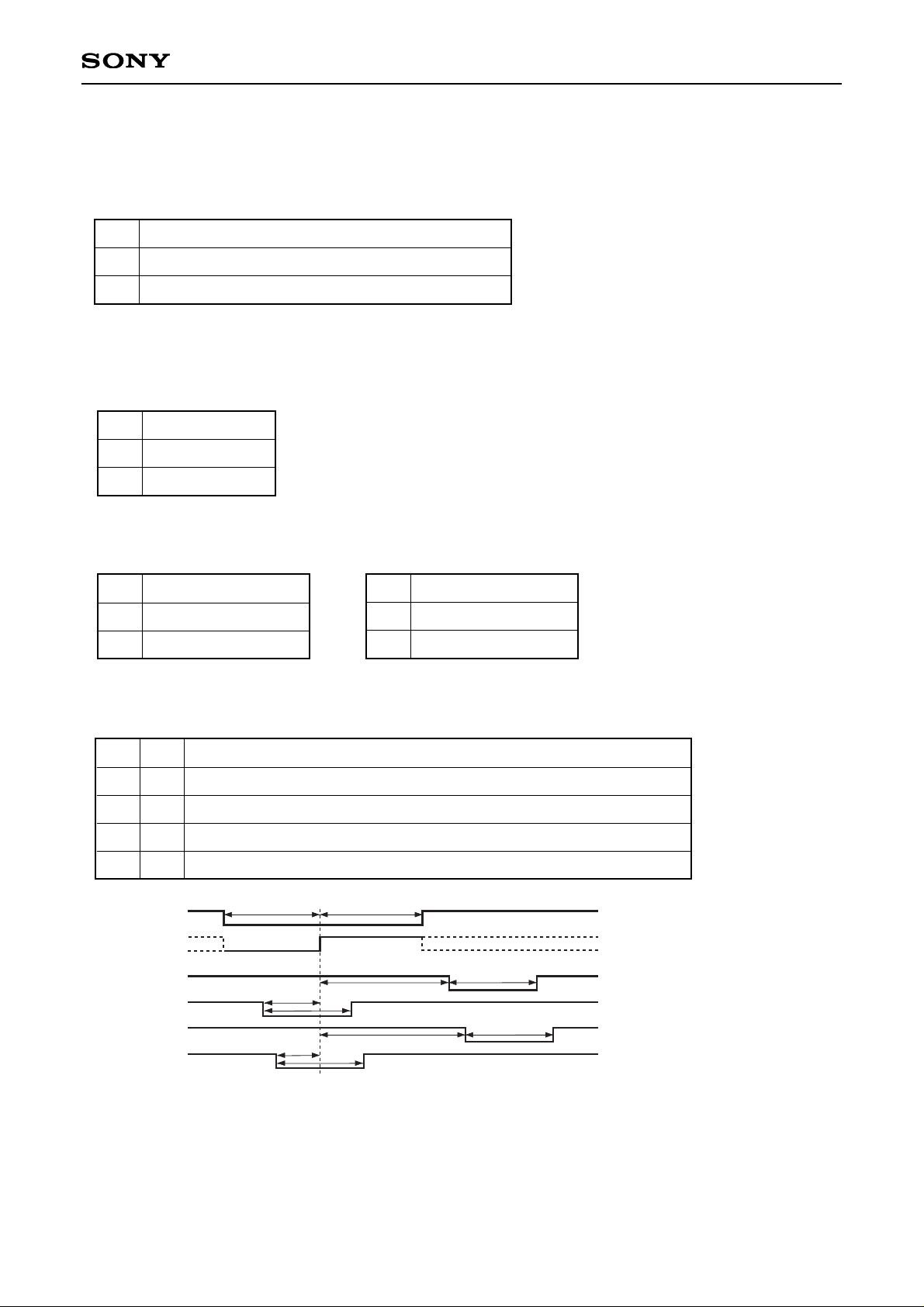
• SLPL
This switches the display system.
D0
0
1
Display system
NTSC
PAL
• SLWD
This switches the display aspect.
D1
0
1
Supported aspect
4:3 display
16:9 display
• SLRGT
This is the right/left inversion function. This switches the horizontal scan direction of the LCD panel.
D4
0
1
Scan mode
Normal display (right scan)
Right/left inverted display (left scan)
• SLDWN
This is the up/down inversion function. This switches the vertical scan direction of the LCD panel.
D5
0
1
Scan mode
Normal display (down scan)
Up/down inverted display (up scan)
• SLSH0, SLSH1, SLSH2
These switch the sample-and-hold timing.
SLSH2
D3
0
0
0
0
1
1
1
1
SLSH1
D2
0
0
1
1
0
0
1
1
SLSH0
D3
0
1
0
1
0
1
0
1
Sample-and-hold position
SHS1
SHS2
SHS3
SHS4
SHS5
SHS6
Through (sample-and-hold off)
Through (sample-and-hold off)
Page 36
– 36 –
CXA3268AR
• SLSYP
This switches the input sync polarity. When using the Pin 4 (SYNC OUT) output as the sync signal (when
using the internal sync separation signals), set this to "0".
D7
0
1
Input polarity
Positive polarity
Negative polarity
• SLHDP, SLVDP
These switch the HDO output and VDO output polarity.
D0
0
1
Output polarity (HDO)
Positive polarity
Negative polarity
D1
0
1
Output polarity (VDO)
Positive polarity
Negative polarity
• SLCP1, SLCP2
These switch the clamp position.
D2
0
1
0
1
D3
0
0
1
1
Clamp position
A (Back porch position/when using the internal sync separation signals)
B (Sync position/when using the internal sync separation signals)
C (Back porch position/during external sync signal input)
D (Sync position/during external sync signal input)
2.35µs
SYNC
RPD
XCLP
B
A
C
D
1.3µs
1µs
2.35µs
2µs
2.9µs
2µs
2µs
2µs
3.6µs
• SLEXVD
This switches the external vertical sync signal (VD/Pin 10) input. This is used when not performing sync
separation with the internal sync separation circuit during external separate sync (VD, HD/Pins 10 and 5)
input. Set to "0" during external CSYNC/Pin 5 input.
D6
0
1
Mode
Other than during external vertical sync signal input
External vertical sync signal input
Note) When clamp is performed at back porch and sync position, set back porch and sync period of Pins 69,
70, 71 and 72 input signals at pedestal level.
Page 37
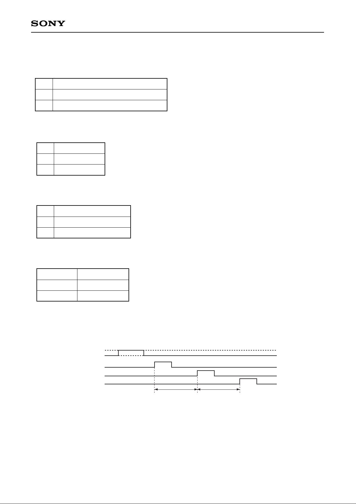
– 37 –
CXA3268AR
• SLFL
This function is used to stop output signal polarity inversion. Normally set to polarity inversion.
D6
0
1
Mode
Polarity inversion
Polarity inversion stopped
• SLTST0, 1, 2, 3, 4
These are the test functions. Set to normal mode.
• HP1, 2, 3, 4, 5
These set the H position. The horizontal display position is switched by adjusting the HST pulse position using
the input horizontal sync signal as the reference. Adjustment is possible in 1 bit = 2fH increments. (1fH = 1 dot)
D0, 1, 2, 3, 4
0
1
Mode
Normal mode
Test mode
Horizontal sync signal
HST
HP: 11111 (LSB)
HP: 10000 (LSB)
HP: 00000 (LSB)
15 steps
(30fH)
16 steps
(32fH)
• SLFR
This function inverts the output signal polarity every field. Normally set to 1H inversion.
D5
0
1
Mode
1H inversion
1 field inversion
• SL4096
This function inverts the output signal polarity every 4096 fields. This further inverts the polarity of the RGB
output that is inverted every 1H for 4096 fields. Normally set to 1H inversion.
D4
0
1
Mode
1H inversion
1H inversion + 4096 field inversion
Page 38

– 38 –
CXA3268AR
• HDP1, 2, 3, 4, 5
These set the HDO output pulse position. The HDO pulse output position is switched using the input horizontal
sync signal as the reference. Adjustment is possible in 1 bit = 4fH increments. (1fH = 1 dot)
Horizontal sync signal
HDO
HDP: 00000 (LSB)
HDP: 11111 (LSB)
31 steps
(124fH)
Page 39
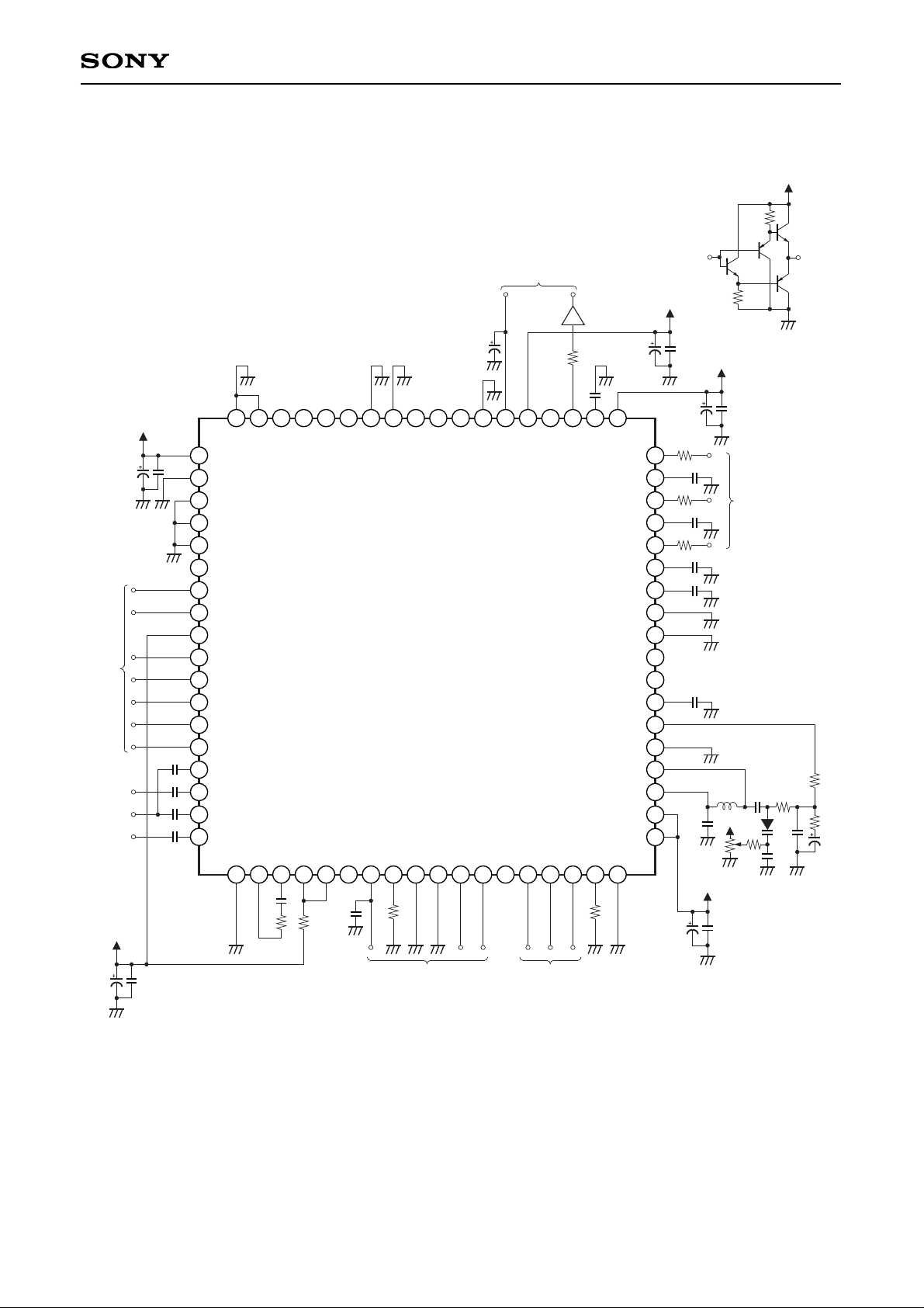
– 39 –
CXA3268AR
Application Circuit (RGB input/Y/color difference input, during internal sync separation signal input)
1µ
270
1µ
Vss
FIL OUT
SYNC IN
SYNC OUT
CSYNC/HD
DA OUT
REF
F ADJ
GND1
VD
DWN
WIDE
TST1
SCK
SEN
SDAT
R INJECT
V
SS
G OUT
G DC DET
R OUT
R DC DET
B OUT
B DC DET
SIG.C
GND2
TST2
HDO
XCLR
VDO
RPD
Vss
CKI
CKO
V
DD
VDD
VDD
TST11
OSD B
OSD R
OSD G
NC
HCK1
HCK2
Vcc1
HST
EN
VCK
VST
RGT
FIL IN
B/B-Y
G/Y
R/R-Y
Vss
Vss
TST10
TST9
TST8
TST7
TST6
TST5
NC
POF
TST4
GND3
COM
Vcc3
TST3
PSIG OUT
PSIG DC DET
Vcc2
+3V
0.01µ
3.3µ 1000p
6800p
33k
1k
10k
3.3µ
0.01µ47µ
+12V
1µ47µ
+12V
1µ47µ
47µ
To LCD Panel
30p
10k
47k
∗
2
∗1 ∗1
∗3
∗1
Resistance value tolerance: ±2%, temperature coefficient: ±200ppm or less
Locate this resistor as close to the IC pin as possible to reduce the effects of external signals.
∗2
Varicap diode: 1T369 (SONY)
∗3
Connect to GND when not using OSD input.
0.1µ
0.01µ
0.68µ
10
0.68µ
15k33k
0.01µ
1k
10
0.68µ
0.68µ
10
10
+3V
0.01µ
47µ
0.01µ
0.01µ
0.01µ
37
38
3940
41
4243
4445
46
4748
49
5051
52
5354
55
56
57
58
59
60
61
62
63
64
65
66
67
68
69
70
71
72
1
2
3 4 5 6
7
8 9 10 11 12 13 14
15
16 17 18
19
20
21
22
23
24
25
26
27
28
29
30
31
32
33
34
35
36
+3V
1µ47µ
To Serial ControllerTo LCD Panel
To LCD Panel
To LCD Panel
B/B-Y
G/Y
R/R-Y
+12V
+12V
22k
Sample PSIG buffer circuit
22k
OUTIN
Buff
Application circuits shown are typical examples illustrating the operation of the devices. Sony cannot assume responsibility for
any problems arising out of the use of these circuits or for any infringement of third party patent and other right due to same.
Page 40
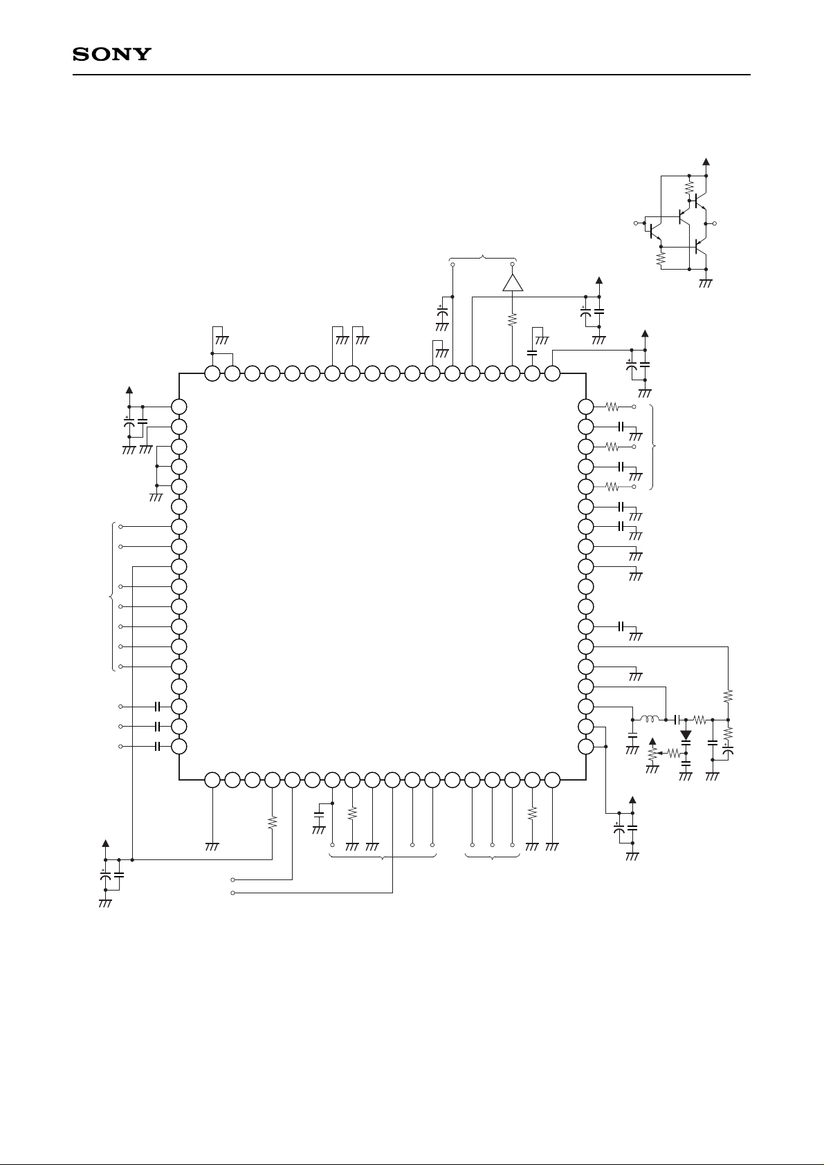
– 40 –
CXA3268AR
Application Circuit (RGB input/Y/color difference input, during external sync signal input)
Vss
FIL OUT
SYNC IN
SYNC OUT
CSYNC/HD
DA OUT
REF
F ADJ
GND1
VD
DWN
WIDE
TST1
SCK
SEN
SDAT
R INJECT
V
SS
G OUT
G DC DET
R OUT
R DC DET
B OUT
B DC DET
SIG.C
GND2
TST2
HDO
XCLR
VDO
RPD
Vss
CKI
CKO
V
DD
VDD
VDD
TST11
OSD B
OSD R
OSD G
NC
HCK1
HCK2
Vcc1
HST
EN
VCK
VST
RGT
FIL IN
B/B-Y
G/Y
R/R-Y
Vss
Vss
TST10
TST9
TST8
TST7
TST6
TST5
NC
POF
TST4
GND3
COM
Vcc3
TST3
PSIG OUT
PSIG DC DET
Vcc2
+3V
0.01µ
3.3µ 1000p
6800p
33k
1k
10k
3.3µ
0.01µ47µ
+12V
1µ47µ
+12V
1µ47µ
47µ
To LCD Panel
30p
10k
47k
∗
2
∗1 ∗1
∗4
∗1
Resistance value tolerance: ±2%, temperature coefficient: ±200ppm or less
Locate this resistor as close to the IC pin as possible to reduce the effects of external signals.
∗2
Varicap diode: 1T369 (SONY)
∗3
Connect to GND when not using OSD input.
∗4
During CSYNC input, input to Pin 5 only (leave Pin 10 open). During separate sync (HD, VD) input, input to Pins 5 and 10.
0.1µ
0.01µ
0.68µ
10
0.68µ
15k33k
0.01µ
100k
CSYNC/HD
VD
10
0.68µ
0.68µ
10
10
+3V
0.01µ
47µ
0.01µ
0.01µ
0.01µ
37
38
3940
41
4243
4445
46
4748
49
5051
52
5354
55
56
57
58
59
60
61
62
63
64
65
66
67
68
69
70
71
72
1
2
3 4 5 6
7
8 9 10 11 12 13 14
15
16 17 18
19
20
21
22
23
24
25
26
27
28
29
30
31
32
33
34
35
36
+3V
1µ47µ
To Serial ControllerTo LCD Panel
To LCD Panel
To LCD Panel
B/B-Y
G/Y
R/R-Y
+12V
∗3
+12V
22k
Sample PSIG buffer circuit
22k
OUTIN
Buff
Application circuits shown are typical examples illustrating the operation of the devices. Sony cannot assume responsibility for
any problems arising out of the use of these circuits or for any infringement of third party patent and other right due to same.
Page 41

– 41 –
CXA3268AR
Notes on Operation
(1) This IC contains digital circuits, so the set board pattern must be designed in consideration of undesired
radiation, interference to analog circuits, etc. Care should also be taken for the following items when
designing the pattern.
• The digital and analog IC power supplies should be separated, but the GND and VSS should not be
separated and should use a plain GND (VSS) pattern in order to reduce impedance as much as possible.
The power supplies should also use a plain pattern.
• Use ceramic capacitors for the by-pass capacitors between the power supplies and GND, and connect
these capacitors as close to the pins as possible.
• The resistor connected to Pin 8 should be connected as close to the pin as possible, and the wiring from
the pin to GND should be as short as possible. Also, do not pass other signal lines close to this pin or the
connected resistor.
• The resistor connected to Pin 17 should be located as close to the pin as possible. Also, do not pass
other signal lines close to this pin.
• The capacitors connected to Pins 7 and 42 should be located as close to the LCD panel as possible.
• The PLL block (LPF/VCO) should be compact and located near the IC.
(2) The R/R-Y (Pin 72), G/Y (Pin 71), B/B-Y (Pin 70) and FIL IN (Pin 69) pin input signals are clamped at the
inputs using the capacitors connected to each pin, so these signals should be input at sufficiently low
impedance.
(Input at an impedance of 1kΩ (max.) or less.)
(3) The smoothing capacitor of the DC level control feedback circuit in the capacitor block connected to the
RGB output pins should have a leak current with a small absolute value and variance. Also, when using the
pulse elimination (PAL display, WIDE display) function, the picture quality should be thoroughly evaluated
before deciding the capacitance value of the capacitor.
(4) A thorough study of whether the capacitor connected to the COM output pin satisfies the LCD panel
specifications should be made before deciding the capacitance value.
(5) If this IC is used in connection with a circuit other than an LCD, it may cause that circuit to malfunction
depending on the order in which power is supplied to the circuits. Thoroughly study the consequences of
using this IC with other circuits before deciding on its use.
(6) Since this IC utilizes a C-MOS structure, it may latch up due to excessive noise or power surge greater than
the maximum rating of the I/O pins, or due to interface with the power supply of another circuit, or due to
the order in which power is supplied to circuits. Be sure to take measures against the possibility of latch up.
(7) Be sure to observe the power supply and power saving sequence specifications specified for this IC.
(8) Do not apply a voltage higher than VDD or lower than VSS to I/O pins.
(9) Do not use this IC under operating conditions other than those given.
(10) Absolute maximum rating values should not be exceeded even momentarily. Exceeding ratings may
damage the device, leading to eventual breakdown.
(11) This IC has a MOS structure which is easily damaged by static electricity, so thorough measures should
be taken to prevent electrostatic discharge.
(12) Always connect the VSS, GND1 and GND2/3 pins to the lowest potential applied to this IC; do not leave
these pins open. The voltages applied to the power supply pins should be as follows.
VSS = GND1 = GND2/3 ≤ VDD = VCC1 ≤ VCC2 = VCC3.
Page 42
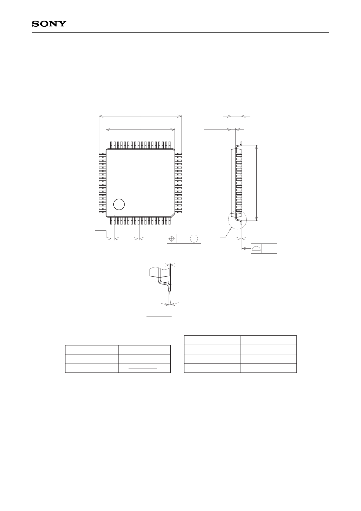
– 42 –
CXA3268AR
SONY CODE
EIAJ CODE
JEDEC CODE
PACKAGE MATERIAL
LEAD TREATMENT
LEAD MATERIAL
PACKAGE MASS
EPOXY RESIN
SOLDER PLATING
42 ALLOY
PACKAGE STRUCTURE
1 18
19
38
3954
72
55
0.5
0.2 ± 0.08
M
0.08
10.0 ± 0.2
12.0 ± 0.3
0.65 ± 0.2
14.5 ± 0.2
11.0 ± 0.2
0.15 ± 0.05
0.1 ± 0.1
0° to 10°
DETAIL A
A
0.1
72PIN LQFP (PLASTIC)
LQFP-72P-L111
P-LQFP72-10X10-0.5
0.3g
Package Outline Unit: mm
 Loading...