

Page 1

—1—
E97640
Sony reserves the right to change products and specifications without prior notice. This information does not convey any license by
any implication or otherwise under any patents or other right. Application circuits shown, if any, are typical examples illustrating the
operation of the devices. Sony cannot assume responsibility for any problems arising out of the use of these circuits.
6ch. Read/Write Amplifier for
Thin Film Head of Hard Disk Drive
24 pin SSOP (Plastic)
CXA3170AN
Description
The CXA3170AN is a Read/Write Amplifier for the
thin film head of hard disk drive and designed to
handle up to 6 channel heads.
Features
• Operate on single +5 V power supply
• Low power consumption
Read : 85 mW
Write : 115 mW + IW ×5
• Designed for two terminal thin-film or MIG heads
• Read amplifier emitter follower output featuring
360 times gain (typ).
• Differential input capacitance for Read : 6 pF (typ)
• Input noise : 0.47 nV / √ Hz (typ)
• Write current range : 5 to 15 mA
• Differential Head voltage swing : 9 Vp-p (typ)
• IW Rise / Fall times : 3.7 ns (typ)
(LH=540 nH, RH=25 Ω, IW=10 mA)
• Differential P-ECL write data input
• Built-in write unsafe detection circuit.
• Built-in Servo write function (3/6 ch).
• Built-in IC protection circuit for short of head and
GND.
• Read data outputs are high impedance in write
mode.
• Unselected head voltage is GND potential.
• Built-in supply voltage monitor circuit prohibits
incorrect write during power on or abnormal
voltage.
• Self switching damping resistance (RD = 360 Ω).
Function
Read, Write and Write unsafe detection for HDD,
power supply ON/OFF detection.
Structure
Bipolar silicon monolithic IC
Absolute Maximum Ratings (Ta=25 °C)
• Supply voltage VCC 6V
•Write current IW 20 mAo-p
• Operating temperature Topr –20 to +75 °C
• Storage temperature Tstg –55 to +150 °C
• Allowable power dissipation
PD 800 mW
• WUS/SE pin input current
ISEH 15 mA
Recommended Operating Conditions
• Supply voltage VCC 5.0 V±10 %
• Write current IW 5 to 15 mAo-p
For the availability of this product, please contact the sales office.
Page 2

—2—
CXA3170AN
DRIVER
AMP
DRIVER
AMP
AMP
DRIVER
AMP
DRIVER
DRIVER
AMP
DRIVER
AMP
1
2
3
4
5
6
7
8
9
10
11
12
H0X
H0Y
H1X
H1Y
H2X
H2Y
H3X
H3Y
H4X
H4Y
H5X
H5Y
GND
R/W
WC
RDY
RDX
HS0
HS1
HS2
WDX
WDY
WUS/SE
V
CC
WRITE
CURRENT
SOURCE
MODE
CONTROL
AMP
HEAD
SELECT
WRITE
UNSAFE
DETECTOR
13
21
22
24
23
20
17
18
19
16
15
14
POWER
ON/OFF
DETECTOR
IC
PROTECTOR
Page 3
—3—
CXA3170AN
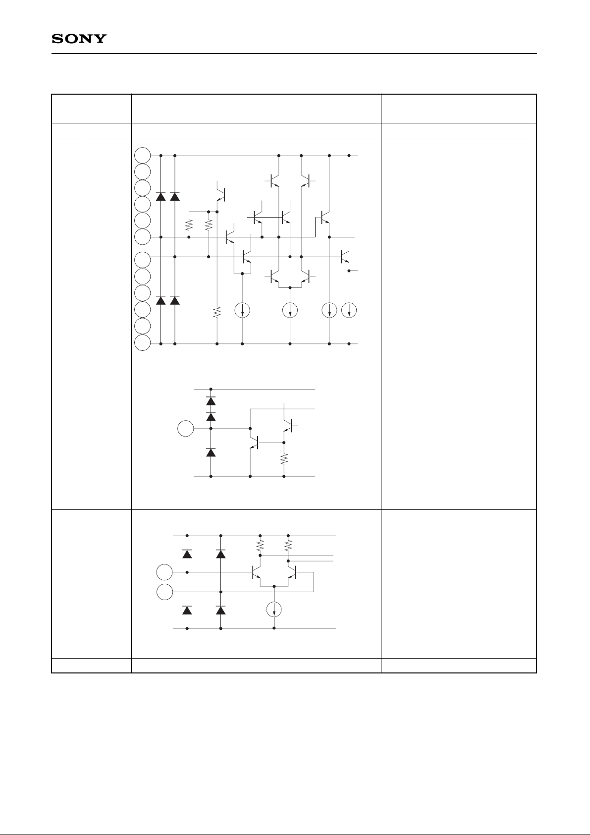
Pin Description
No.
24
1
2
3
4
5
6
7
8
9
10
11
12
14
15
16
13
Symbol
GND
H0X
H0Y
H1X
H1Y
H2X
H2Y
H3X
H3Y
H4X
H4Y
H5X
H5Y
WUS/SE
WDY
WDX
VCC
Equivalent circuit
1
3
5
7
9
11
2
4
6
8
10
12
2k 2k
VCC
GND
100K
Description
Head.
6 channels provided.
Write unsafe detection output /
Servo Enable signal input.
Differential P-ECL write data
input.
5 V power supply.
14
VCC
GND
16
VCC
GND
15
Page 4
—4—
CXA3170AN
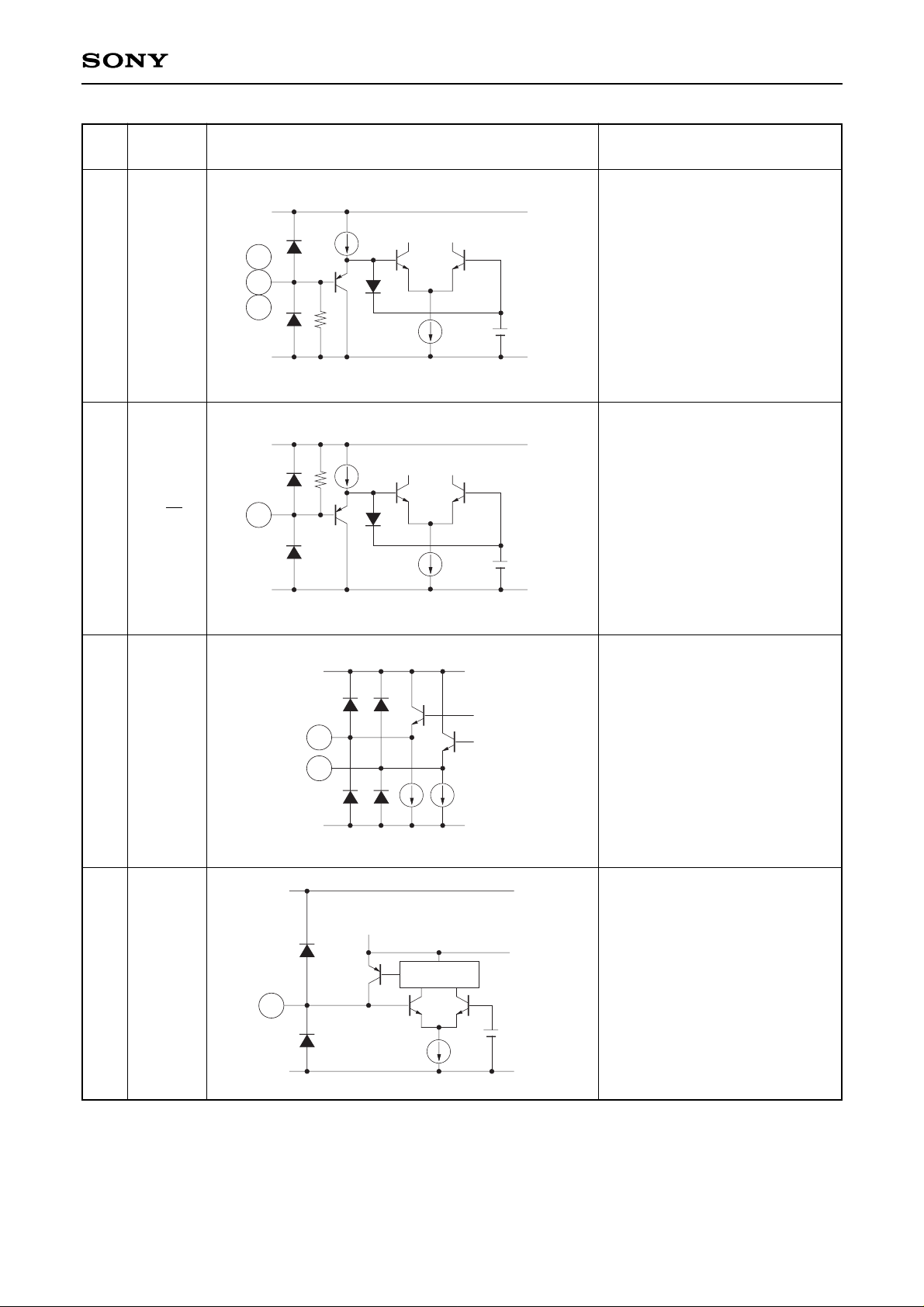
No.
17
18
19
23
20
21
22
Symbol
HS2
HS1
HS0
R/W
RDX
RDY
WC
Equivalent circuit
VCC
GND
17
18
19
100k
2.1V
VCC
GND
100k
2.1V
23
VCC
GND
21
20
VCC
GND
22
2.5V
Description
Head select signal input.
Selects one of 6 heads according
to Table 2.
Read/Write signal input
At “High” : Read,
at “Low” : Write.
Read Amplifier output.
A setting resistor for the write
current value is connected
between this pin and GND.
Page 5
—5—
CXA3170AN
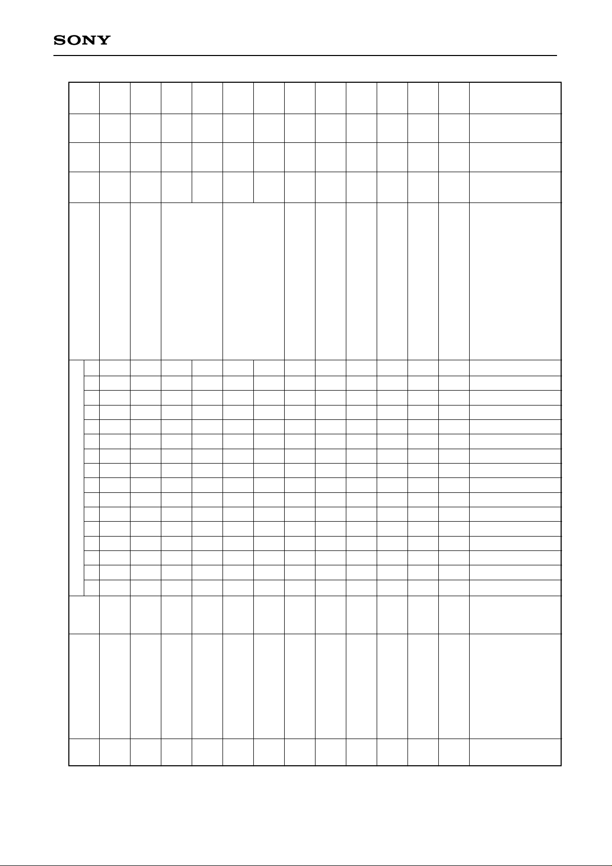
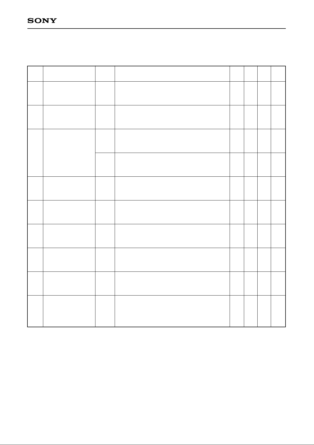
Electrical Characteristics (Unless otherwise specified, VCC=5 V, Ta=25 °C, Write current IW=15 mA)
No.
1-1
1-2
2-1
2-2
2-3
2-4
2-5
2-6
2-7
2-8
3-1
3-2
4
Item
Current consumption
for Read
Current consumption
for Write
Digital input “Low”
input voltage
Digital input “High”
input voltage
Digital input “Low”
input current
Digital input “High”
input current
Write data input
“Low” input voltage
Write data input
“High” input voltage
Write data
input current
Unselected
head voltage
Write unsafe output
saturation voltage
Write unsafe output
leak current
Supply power
ON/OFF detector
threshold voltage
Symbol
I
R
IWR
VIL
VIH
IIL
IIH
VWDL
VWDH
IWD
Vunsel
VWUS
IWUS
VTH
SW conditions
1 2 3 4 5 6 7 8 9 10 11 12 13 14 15 16
a a a a a a e b a a b a a a b b
a a a a a a e b a a b a a a b a
a a a a a a e b a a b a a a b a
a a a a a a e b a a b b b b b b
a a a a a a e b a a b a a a a a
b a a a a a b b a c c a a a b a
a a a a a a e b a a b a a a b a
b a a a a a a b a a b a a a b a
Measurement conditions
Test point : l
2
Test point : l2
Digital input :
Pins 17, 18, 19, 23
“High” applied voltage : 5 V
“Low” applied voltage : 0 V
Test point : l6, l7, l8, I9
Input voltage : 4 V
Output current : 1 mA
Test point : V1
Test point : l
3
When VCC is lowered from 5 V in
Write mode and IW does not flow
anymore, VCC voltage is set to
VTHOFF. When VCC is raised from
3 V and IW starts to flow, VCC
voltage is set to VTHON.
Min. Typ. Max. Unit
11 17 26 mA
16 22 36
mA
+IW +IW +IW
0.8 V
2.0 V
–100 µA
100 µA
VWDH VWDH
V
–2.0 –0.25
VCC VCC
V
–1.1 –0.4
50 µA
0.3 V
0.5 V
50 µA
3.4 3.9 4.3 V
Page 6
—6—
CXA3170AN
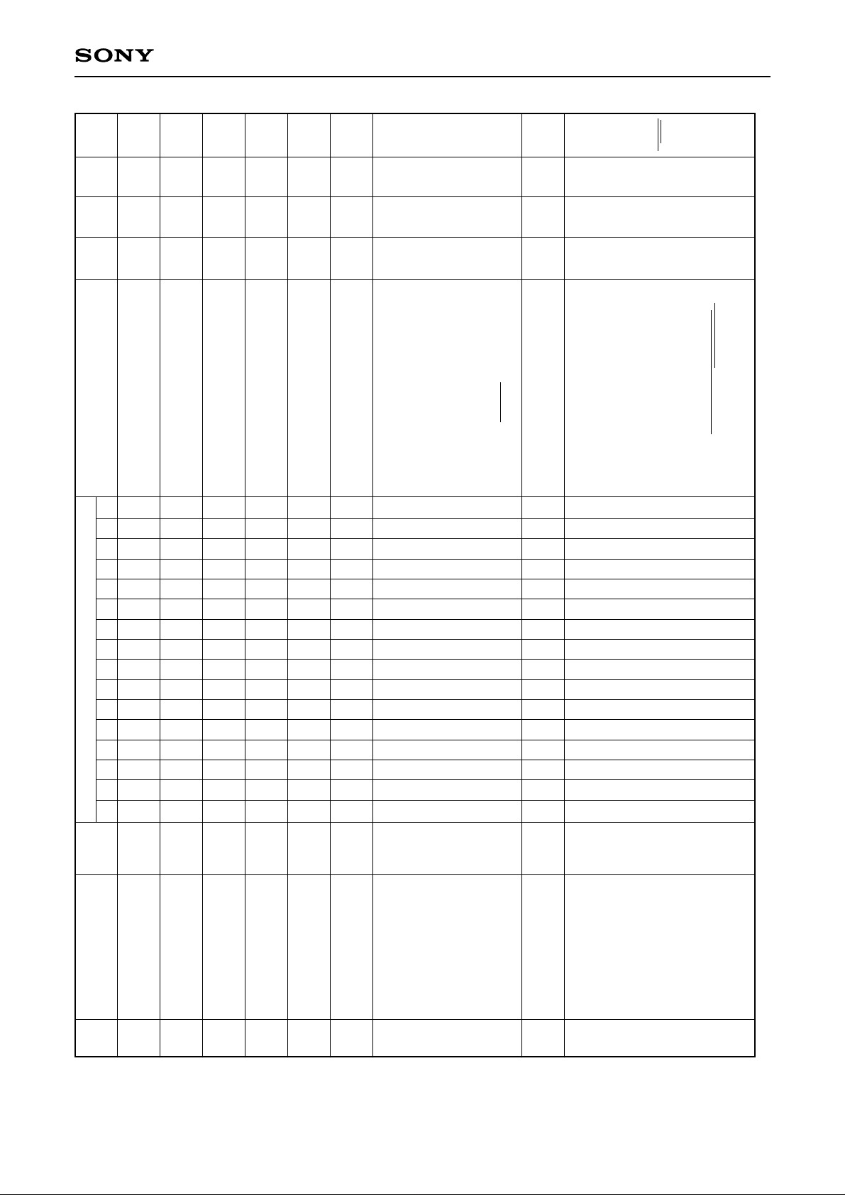
No.
5-1
5-2
5-3
5-4
6-1
6-2
7
8
9
Item
Write current
setting range
Write current voltage
Write current gain
Write current
setting constant
WUS/SE voltage
WUS/SE sink current
Read amplifier
differential voltage
gain
Frequency band
width (–3 dB)
Input referred noise
Symbol
I
W
VWC
AW
KW
VSEH
ISEH
AV
BW
EN
SW conditions
1 2 3 4 5 6 7 8 9 10 11 12 13 14 15 16
a a a a a a e b a a b a a a a a
b a a a a a a b a a b a a a b a
b a a a a a a b b a a a a a b a
b a a a a a a b b a a a a a b a
b a a a a a c b a a b a a a b b
b a a a a a c b a a b a a a b b
a a a a a a e b a a b a a a b b
Measurement conditions
I
W=AW • VWC/RWC
IW=KW/RWC
Servo write enabled
Servo write enabled
Input voltage SG1 :
1 mVp-p, 300 kHz
Load resistance (RDX, RDY) :
1 kΩ
Test point : V4 [Vp-p]
AV =
V4
SG1
Frequency at which AV lowers
by 3 dB
Head impedance : 0 Ω,
when the read amplifier output
voltage is amplified 100 times
and voltage passed though a
LPF (low pass filter of cutoff
frequency 15 MHz) is VN [Vrms],
EN =
VN
100 • AV√ 15 × 10
6
Test point : V5
Min. Typ. Max. Unit
5 15 mAo-p
2.25 2.5 2.75 V
18 20 22
mA/mA
45 50 55
VCC VCC V
+1.5 +1.6
5 14 mA
305 360 415 V/V
100 140 MHz
nV
0.47 0.6
√ Hz
Page 7

—7—
CXA3170AN
No.
10
11
12
13
Item
Common mode
rejection ration
Power supply
rejection ratio
Channel
separation
Read data output
offset voltage for Read
Symbol
CMRR
PSRR
CS
V
OFFR
SW conditions
1 2 3 4 5 6 7 8 9 10 11 12 13 14 15 16
b a a a a a d b a a b a a a b b
a a a a a a e a a a b a a a b b
a b a a a a c b a a b a a a b b
a a a a a a e b a a b a a a a b
Measurement conditions
In-phase input voltage
SG2 : 100 mVp-p, 20 MHz
When the Read amplifier output
is V
CM [mVp-p],
100
CMRR = 20 log
VCM
+20 log AV
Test point : V4
Ripple voltage SG3 :
100 mVp-p, 20 MHz
When the Read amplifier output
is VP [mVp-p],
100
PSRR = 20 log
VP
+20 log AV
Test point : V4
Selected head input voltage
: 0 mVp-p
Unselected head input voltage
SG1 : 100 mVp-p, 20 MHz
When the Read amplifier output
is VCS [mVp-p],
100
CS = 20 log
VCS
+20 log AV
Test point : V4
VOFFR = V2–V3
Test point : V2, V3
Min. Typ. Max. Unit
50 dB
50 dB
50 dB
–250 250 mV
Page 8

—8—
CXA3170AN
No.
14
15
Item
RDX, RDY common
mode output voltage
difference between
modes
RDX, RDY common
mode output voltage
for Read
Symbol
Vdiff
V
RD
SW conditions
1 2 3 4 5 6 7 8 9 10 11 12 13 14 15 16
a a a a a a e b a a b a a a b c
a a a a a a e b a a b a a a a b
Measurement conditions
Test point : Pin 20, 21
Test point : V
2, V3
Min. Typ. Max. Unit
–300 300 mV
V
CC VCC VCC
V
–2.6 –2.3 –2.0
Page 9
—9—
CXA3170AN
Unless otherwise specified, VCC=5 V, Ta=25 °C, fWD (Write data frequency) =5 MHz, IW=15 mA, LH (Head
inductance) =1 µH, RH (Head DC resistance value) =30 Ω
Refer to Fig. 2 to Fig. 4
No.
14
15-1
15-2
16-1
16-2
17
18
19-1
19-2
Item
Head differential
voltage amplitude
Mode switching time
Read to Write
Mode switching time
Write to Read
Mode switching time
safe to unsafe
Mode switching time
unsafe to safe
Head switching time
Write current
propagation delay
time
Write current
rise/fall time
Write current
rise/fall time
Measurement conditions
Differential voltage between HX pin and HY pin
at switching of Write current
TRW is the time required for Write current to turn
to 90 % after Pin 23 changes from “High” to
“Low”.
TWR1 is the time required for the Read amplifier
output∗to turn to 90 % after Pin 23 changes
from “Low” to “High”.
TWR2 is the time required for Write current to
decreases to 10 % after Pin 23 changes from
“Low” to “High”.
TSA1 is the time required for Pin 14 to turn
“High” after the last transition of Write data
when Write data is stopped in Write mode.
TSA2 is the time required for Pin 14 to turn “Low”
after the first transition of Write data in Write
mode.
TH is the time required for the Read amplifier
output∗ to reach 90 % when the selected head
switched in Read mode.
TPD is the time required for Write current to
reach 90 % after the Write data falling edge.
TR is the time required for Write current to reach
90 % from 10 %; TF is the same time required
to reach 10 % from 90 %. LH=0 µH, RH=0 Ω
LH=540 nH, RH=25 Ω, IW=10 mA
TR is the time required for Write current to reach
90 % from 10 %; TF is the same time required
to reach 10 % from 90 %.
Symbol
VSW
TRW
TWR1
TWR2
TSA1
TSA2
TH
TPD
TR/TF
TR/TF
Min. Typ. Max. Unit
9 Vp-p
130 150 ns
180 220 ns
100 200 ns
1.0 2.3 3.0 µs
0.6 µs
0.6 µs
2 7 ns
1 3 ns
3.7 ns
∗Read amplifier output 100 mVp-p 10 MHz
Page 10

—10—
CXA3170AN
Test Circuit 1
A
3.3k
I9
a
b
A
I8
a b
A
I7
a b
A
I6
a b
A
I5
ab
A
I4
A
I3
a bb ba a
S14 S13 S12 S11 S10 S9
c abc
1324 23 22 192021 1415161718
V4
5V
V3 V2
1µ 1µ
V
×100
×1
AMP
AMP
V5
V
LPF
to15MHz
3V
PG
SG5 SG4
PG
4V
1µ
5.1k
a b
VCC
5V
SG3
VCC
5V
A
I2
V
V1
S8
S1
a b a bS2a b a bS3a b a bS4a b a bS5a b a bS6a b a b
2 3 4 5 6 7 8 9
10 11 12
1
S7
a b c d e
A
I1
33
SG1
0.1µ 0.1µ
0.1µ
a b c d e
SG2
S15
S16
V V
c
PG
SG6
A
I14
6.5V
Test Circuit 2
3.3k
1µ
×1
AMP
1µ
LH
1µH
LH
1µH
LH
1µH
LH
1µH
LH
1µH
LH
1µH
2 3 4 5 6 7 8 9
10 11 12
1
PG
1µ
PG PG PG
1324 23 22 192021 1415161718
5V
1k 1k
5.1k
Fig. 1
Fig. 2
Page 11
—11—
CXA3170AN
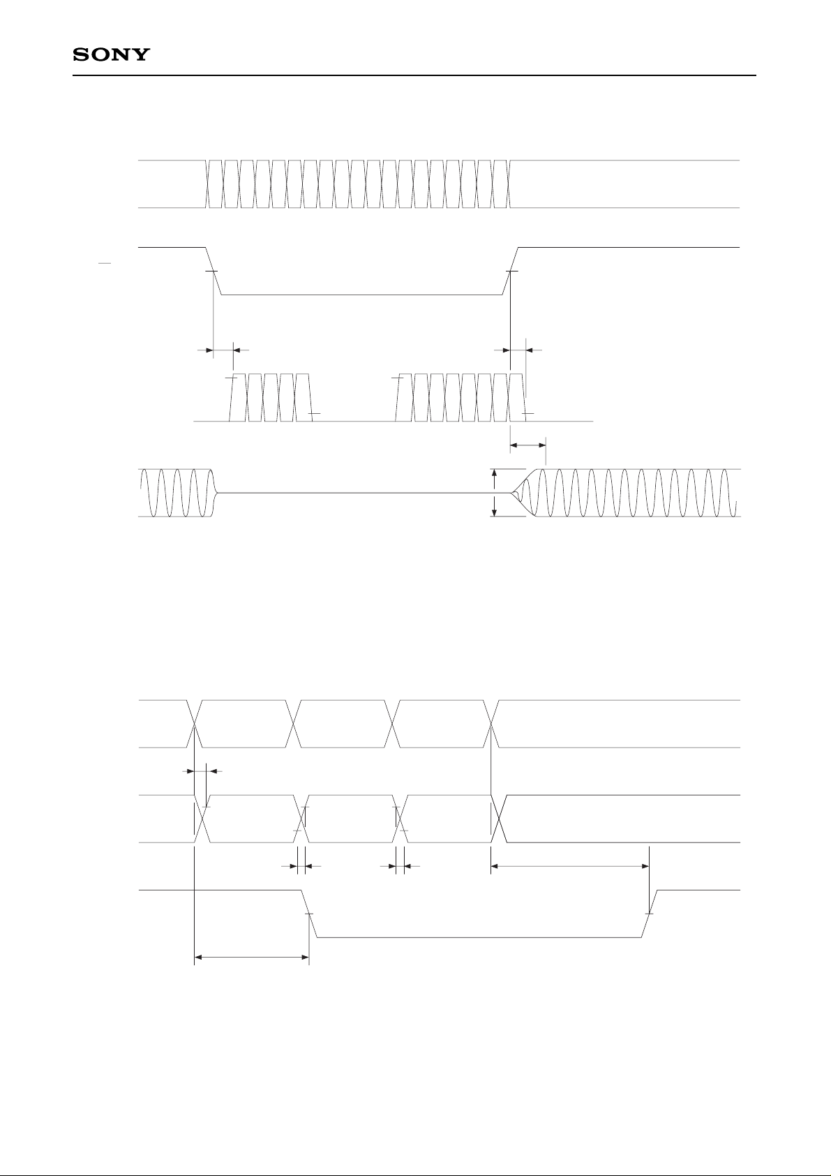
Timing Chart 1
50% 50%
TRW TWR 2
10% 10%
TWR1
90%
WDX
WDY
I
WX
IWY
RDX
RDY
90% 90%
R/W
Fig. 3
Fig. 4
Timing Chart 2
TPD
90% 90% 90%
10% 10%
TR TF
50%
TSA2
TSA1
50%
WDX
WDY
I
WX
IWY
WUS
Page 12

—12—
CXA3170AN
Description Functions
Read amplifier
This is a low noise amplifier for amplifying the signals from the heads with an emitter follower output.
The RDX and RDY are the outputs of the differential amplifier whose polarity between the RDX and X side of
the head input is same.
Write circuit
The Write data input to WDX pin and WDY pin passes through the buffer amp. It drives the Write switch
circuit which supplies the Write current to the heads.
The Write current flows into the X side when WDX is “Low” and WDY is “High”.
Mode control
The mode are set as shown Table 1 by R/W and WUS/SE.
Table 1. Mode selection
Head selection
The heads are selected as shown in Table 2 by the HS0, HS1 and HS2 pins.
Table 2. Head selection
Servo write mode ∗∗
This mode allows for writing to multiple channels at once.
To enable servo write mode follow these steps:
(1) Place the device in the Read mode.
(2) Set HS0 and HS1 following Table 3.
(3) Set WUS/SE to VSEH, or input ISEH to WUS/SE.
(4) While maintaing step (2) and (3) above make R/W low, placing the device in servo write mode.
R/W
L
H
L
WUS/SE
X
X
∗∗
HS0 HS1 HS2
See Table 2
See Table 3 X
Mode
Write
Read
Servo Write
HS0
L
H
L
H
L
H
HS1
L
L
H
H
L
L
HS2
L
L
L
L
H
H
Head
0
1
2
3
4
5
Page 13

—13—
CXA3170AN
Write unsafe detection circuit
This circuit detects write errors.
In normal Write mode, the WUS output is low; in the conditions listed below, it is high.
• Head inputs is open (under the condition which. RH=∞ and Write data frequency is ≤ 10 MHz)
• Head input is shorted to GND or VCC.
• Write data frequency is abnormally low.
• No write current.
• In read mode.
• Supply voltage is abnormal (see power supply ON/OFF detection).
Power supply ON/OFF detection
This circuit monitors VCC to detect erroneous Writes. The error status is established when VCC falls below the
threshold voltage (VTH) of the power supply ON/OFF detector, in which case the recording and playback
functions are prohibited. When VCC rises above, VTH, the prohibition of these functions is released.
Table 3. Head selection in Servo Write mode
HS0
L
H
L
H
HS1
L
L
H
H
Head
0, 1, 2
0, 1, 2, 3, 4, 5
3, 4, 5
0, 1, 2, 3, 4, 5
Page 14
—14—
CXA3170AN
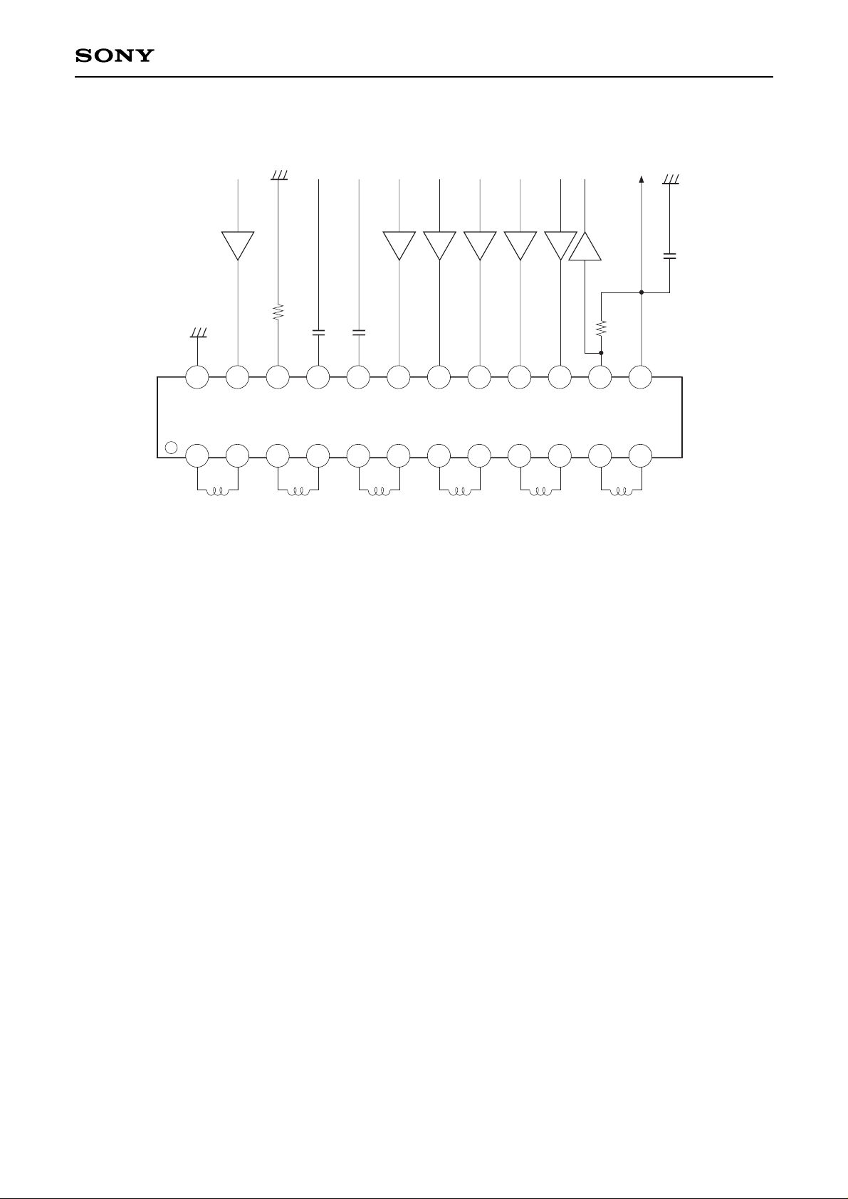
Application Circuit
3.3k
1µ
LH
1µH
LH
1µH
LH
1µH
LH
1µH
LH
1µH
LH
1µH
5.1k
R
WC
+5V
2 3 4 5 6 7 8 9
10 11 12
1
1324 23 22 192021 1415161718
Application circuits shown are typical examples illustrating the operation of the devices. Sony cannot assume responsibility for
any problems arising out of the use of these circuits or for any infringement of third party patent and other right due to same.
Page 15

—15—
CXA3170AN
Notes on operation
• This device handles high frequency and high gain signals. Please note the following;
♦ Connect VCC decoupling capacitor of approximately 1000 pF near the device.
♦ Make the GND area as large as possible.
• When using as 2 or 4-channel, short-circuit the X and Y sides of unused head pins or leave them open.
• The WC pin is a constant voltage pin. When noise affects this pin, it creates noise in Write c current.
Therefore, locate RWC as close to the device as possible.
• Write unsafe detection circuit
This circuit uses the voltage waveforms of the head pins for detection.
♦ VFB must be more than 2 V. When VFB < 2 V, it is possible that Write unsafe detection maximum
frequency becomes more than 1 MHz.
♦ The normal operating area of write unsafe detection circuit is changed by head inductance, head DC
resistance, write current and other.
VTH
GND
Voltage waveform
of head pins (HX, HY)
VTH=1.4VVFB
Wave form of write data
Page 16

—16—
CXA3170AN
Application Notes
Use the following characteristics for reference. VCC=5 V, Ta=25 °C
Item
Write mode
Differential output capacitance
Differential output resistance
Differential input capacitance
Read mode Differential input resistance
Output resistance
Unselected head differential current in Write
mode
Write current symmetry
Symbol
CO
RO
CI
RI
RRD
IUS
TAS∗
Conditions
Between head input pins
Between head input pins
f=5 MHz
RDX or RDY, f=5 MHz
LH=1 µH, RH=30 Ω
IW=15 mA
LH=0 µH, RH=0 Ω
IW=15 mA
Min. Typ. Max. Unit
4.5 6 pF
260 360 470 Ω
6 10 pF
650 1500 3000 Ω
50 Ω
0.2 mAp-p
–0.5 0.5 ns
IWX+IWY 50% 50% 50%
T1 T2
Fig.5 Write current vs. RWC
I
W
-Write current (mA)
5 10 152
5
R
WC (kΩ)
Fig.6 Write current setting constant vs. Write current
Write current setting constant K
55
52.5
50
47.5
45
4 6 8 10 12 14 16
Write Current I
W (mA)
K=RWC ·IW
20
10
22
WC
R
WC
∗TAS=T1–T2
Setting of Write current
Write current can be set with resistor RWC (kΩ) at Pin 22.
IW=K/RWC (mA) Refer to Fig. 5.
Page 17

—17—
CXA3170AN
Normalized write current
vs. Supply voltage
1.04
1.02
1
0.98
0.96
I
W
/I
W
(V
CC
=5V)
4 5 6
Supply voltage V
CC [V]
Ta=25°C
R
WC=3.3kΩ
1.04
1.02
1
0.98
0.96
I
W
/I
W
(Ta=25°C)
–25 25 75
Ambient temperature Ta [°C]
V
CC=5V
RWC=3.3kΩ
0 50
1.04
1.02
1
0.98
0.96
A
V
/A
V
(V
CC
=5V)
4 5 6
Supply voltage V
CC [V]
Ta=25°C
1.04
1.02
1
0.98
0.96
A
V
/A
V
(Ta=25°C)
–25 25 75
Ambient temperature Ta [°C]
0 50
4
3.6
Power supply ON/OFF Detector
Threshold Voltage [V]
–25 25 75
Ambient temperature Ta [°C]
Normalized write current
vs. Ambient temperature
Normalized read amplifier voltage tgain
vs. Supply voltage
Normalized read amplifier voltage gain
vs. Ambient temperature
Power supply ON/OFF detector threshold
voltage vs. Ambient temperature
0 50
3.8
4.2
OFF ON
→
ON OFF
→
V
CC=5V
Page 18

SONY CODE
EIAJ CODE
JEDEC CODE
SSOP-24P-L01
SSOP024-P-0056
PACKAGE MATERIAL
LEAD TREATMENT
LEAD MATERIAL
PACKAGE MASS
EPOXY RESIN
SOLDER/PALLADIUM
42/COPPER ALLOY
PACKAGE STRUCTURE
PLATING
0.1g
24PIN SSOP(PLASTIC)
∗5.6 ± 0.1
24
∗7.8 ± 0.1
13
0.65
12
1
0.22 – 0.05
+ 0.1
0.15 – 0.02
+ 0.05
7.6 ± 0.2
0.1
1.25 – 0.1
+ 0.2
A
0.1 ± 0.1
0° to 10°
0.5 ± 0.2
DETAIL
A
NOTE: Dimensions “∗” does not include mold protrusion.
0.13
M
Package Outline Unit : mm
CXA3170AN
—18—
NOTE : PALLADIUM PLATING
This product uses S-PdPPF (Sony Spec.-Palladium Pre-Plated Lead Frame).
 Loading...