

Page 1
Laser Driver
Description
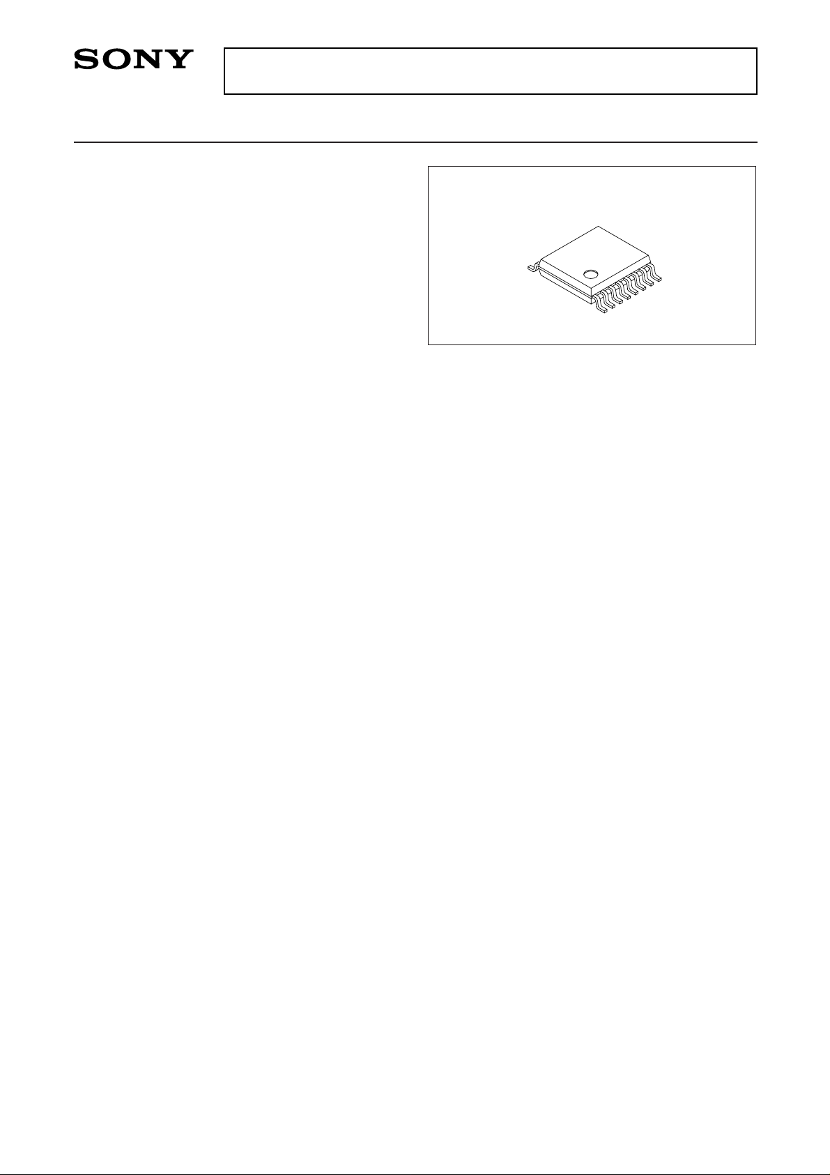
The CXA2610N is a laser driver IC for optical discs.
This IC supports higher optical power output speeds.
Features
• LD driver with excellent driving capability
• Write current of 250mA (max.) possible by setting
the IIN2 (Pin 2) and IIN3 (Pin 5) external resistors
• Rise time ≈ 3ns
• Fall time ≈ 4ns
• The oscillation frequency of the built-in oscillation
circuit can be set from 100 to 600MHz by
connecting the OSCFR (Pin 4) external resistor to
GND.
• The oscillator amplitude initial value of the built-in
oscillation circuit can be set by connecting the
OSCGA (Pin 12) external resistor to GND, and the
oscillator amplitude can be adjusted by the IINR
input current value.
• Oscillation ON/OFF can be set as desired.
• Single +5V power supply
• TTL/CMOS control for control system
Applications
• CD-R driver
• CD-RW driver
• DVD driver
• Writable optical driver
• Laser diode current switching
Structure
Bipolar silicon monolithic IC
Absolute Maximum Ratings
• Supply voltage Vcc 5.5 V
• Operating temperature Topr –10 to +70 °C
• Storage temperature Tstg –65 to +150 °C
Operating Conditions
Supply voltage 4.5 to 5.5 V
– 1 –
E99320-PS
Sony reserves the right to change products and specifications without prior notice. This information does not convey any license by
any implication or otherwise under any patents or other right. Application circuits shown, if any, are typical examples illustrating the
operation of the devices. Sony cannot assume responsibility for any problems arising out of the use of these circuits.
CXA2610N
16 pin SSOP (Plastic)
Page 2

– 2 –
CXA2610N
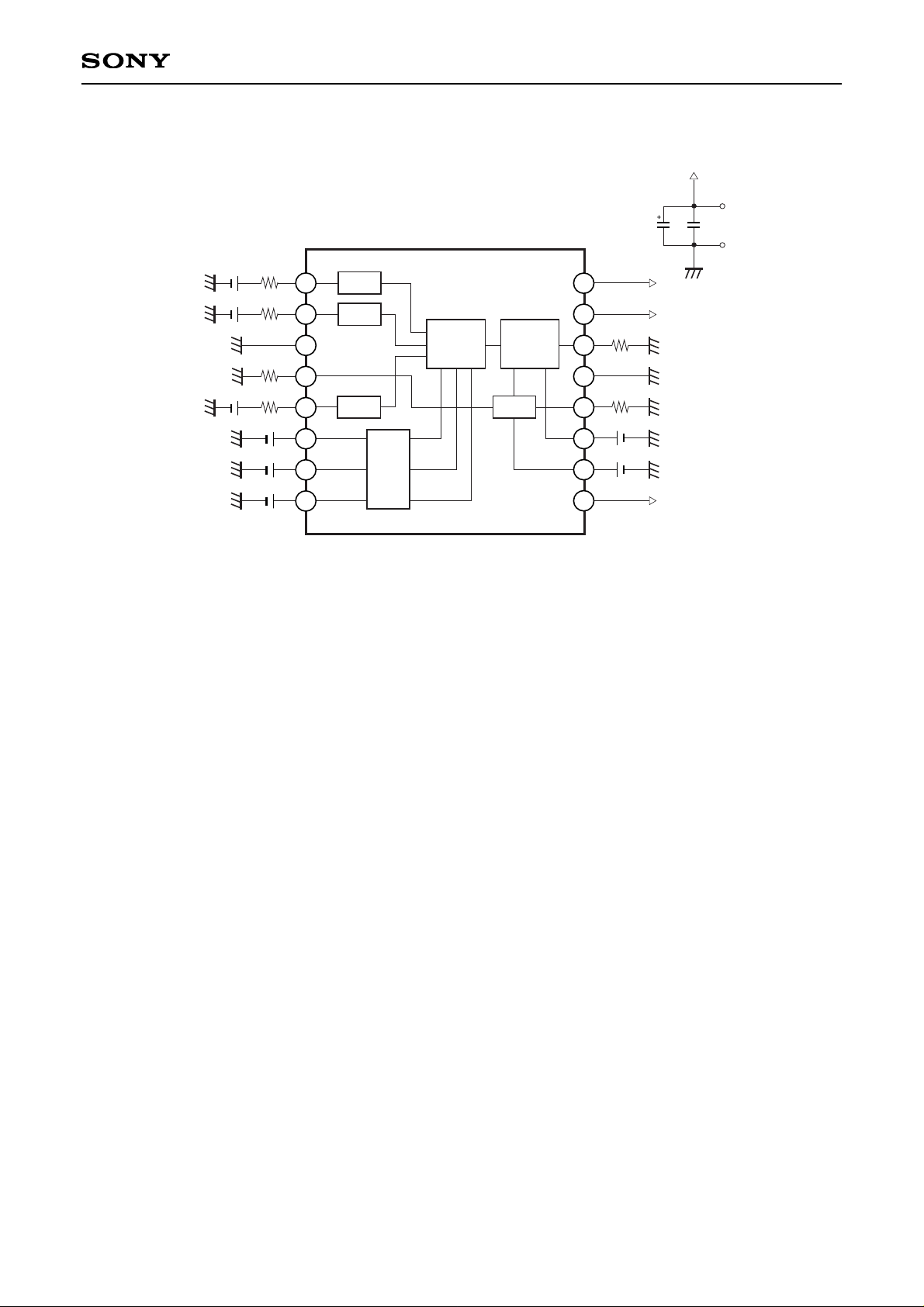
Pin Description
Pin
No.
1
2
3
4
5
6
7
8
9
10
11
12
13
14
15
16
Symbol
IINR
IIN2
GND
OSCFR
IIN3
CONTR
CONT2
CONT3
Vcc
OSCENA
ENABLE
OSCGA
GND
LD0
Vcc
Vcc
I/O
I
I
—
I
I
I
I
I
—
I
I
I
—
O
—
—
Description
Oscillation level adjustment.
LD drive current setting input.
Ground.
Oscillation frequency adjustment.
LD drive current setting input.
LD drive current output setting.
LD drive current output setting.
LD drive current output setting.
VCC.
Oscillation ON for read/forced oscillation ON control.
LD drive current ON/OFF control. (High: ON, Low: OFF)
Oscillation level initial value setting.
Ground.
LD anode side connection.
VCC.
VCC.
V-I
V-I
V-I
TTL
1
2
3
4
5
6
7
8
9
10
11
12
13
14
15
16
OSC
Driver
Current
SW
Vcc
Vcc
LD0
GND
OSCGA
ENABLE
OSCENA
Vcc
IINR
IIN2
GND
OSCFR
IIN3
CONTR
CONT2
CONT3
Block Diagram
Page 3

– 3 –
CXA2610N
OSC: L (write mode). LD: OFF
Current consumption for IINR input voltage where oscillation level =
47mAp-p
Current consumption when CONTR = Low for I
CC2 (OSC: ON)
Pin voltage measurement
Pin voltage measurement
Output current for IINR pin input 5V
Output current for IIN2 pin input 5V
Output current for IIN3 pin input 5V
Current gain measurement for IINR (∆I
OUT/∆IIN)
Current gain measurement for IIN2 (∆I
OUT/∆IIN)
Current gain measurement for IIN3 (∆I
OUT/∆IIN)
IOUT = 40mA (CONTR) + 40mA (CONT2), settling 10 to 90%
I
OUT = 40mA (CONTR) + 40mA (CONT2), settling 10 to 90%
I
OUT = 40mA (CONTR) + 40mA (CONT2)
Time from 50% of CONT3 (High
→ Low) to 50% of output final value
Time from 50% of CONT3 (Low → High) to 50% of output final value
Time from 50% of ENABLE (Low → High) to 50% of output final value
Time from 50% of ENABLE (High → Low) to 50% of output final value
Oscillation frequency
Oscillation level when IINR = 2V
CONTR, CONT2, CONT3, OSCENA, ENABLE
CONTR, CONT2, CONT3, OSCENA, ENABLE
Input impedance for IINR, IIN2 and IIN3
20
35
50
1.21
80
115
145
14595120
120
60
2
175
35
55
78
1.257
103
125
157
163
104
133
136
3
4
—
3.1
3.4
4.4
2.2
189
77
252
52
75
105
1.3
120
145
175
175
115
145
145
85
1.3
375
mA
mA
mA
V
mV
mA
mA
mA
—
—
—
ns
ns
%
ns
ns
ns
ns
MHz
mAp-p
V
V
Ω
1
2
3
4
5
6
7
8
9
10
11
12
13
14
15
16
17
18
19
20
21
22
23
Current consumption 1
Current consumption 2
Current consumption 3
Pin voltage 1
Pin voltage 2
Output drive current
Output drive current
Output drive current
Input/output current gain
Input/output current gain
Input/output current gain
Rise time
Fall time
Overshoot
CONT delay 1
CONT delay 2
LD delay 1
LD delay 2
Oscillation frequency
Oscillation level
Logic Low level
Logic High level
Input resistance
I
CC1
ICC2
ICC3
VFR
VLE
I
OUT1IOUT2IOUT3IGAIN1IGAIN2IGAIN3
TR
TF
OVS
CDELAY1
CDELAY2
LDELAY1
LDELAY2
OSCFR
OSCLE
VTHL
VTHH
ZIN
2.0
1.3
—
—
1.3
2.0
1.3
2.0
1.3
2.0
1.3
1.3
—
—
—
2.0
—
—
2.0
1.3
2.0
2.0
1.3
2.0
H → L
L → H
H → L
1.3
2.0
2.0
—
—
—
2.0
—
—
2.0
1.3
2.0
1.3
2.0
H → L
H → L
2.0
—
—
—
1.3
2.0
1.3
2.0
1.3
2.0
2.0
1.3
2.0
—
—
—
1.3
2.0
2.0
2.0
L → H
H → L
2.0
—
—
—
Measure-
ment No.
Measurement item Symbol
CONTR CONT2 CONT3
OSCENA
ENABLE
Control status
Measurement condition and method Min. Typ. Max. Unit
Electrical Characteristics (Ta = 25°C, Vcc = 5V)
AC items
Logic
Page 4
– 4 –
CXA2610N
Electrical Characteristics Measurement Circuit
V-I
3.9kΩV1
V-I
V-I
TTL
1
2
3
4
5
6
7
8
9
10
11
12
13
14
15
16
OSC
Driver
Current
SW
Vcc
GND
ENABLE
OSCENA
IINR
IIN2
IIN3
CONTR
CONT2
CONT3
3.9kΩV2
3.9kΩV5
V6
V7
V8
4.3kΩ
V11
10Ω
22µ 0.1µ
20Ω
V10
Page 5
– 5 –
CXA2610N
Description of Functions
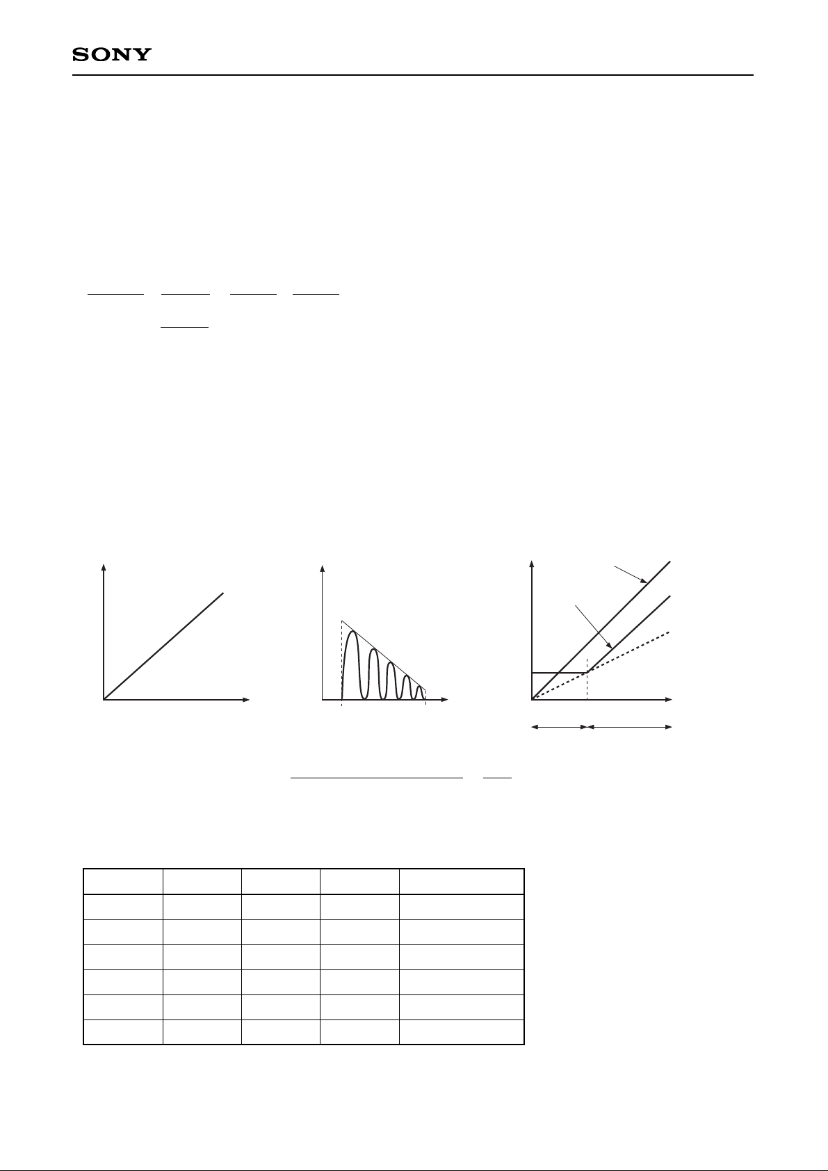
(1) LD drive current value setting
The current controlled by the current setting pins IINR, IIN2 and IIN3 is output from the LD0 pin.
The current flowing to the LD0 pin can be set independently for IINR, IIN2 and IIN3 by CONTR, CONT2 and
CONT3.
(2) LD drive current forced OFF
Forced OFF is enabled by setting the ENABLE pin Low.
(3) Oscillation circuit
The oscillation circuit is turned ON forcibly by setting the OSCENA pin Low.
(OSCENA × CONTR × (CONT2 + CONT3))
The oscillation circuit is turned ON by setting the OSCENA pin High only for read.
(OSCENA × CONTR × CONT2 × CONT3)
(4) Oscillation frequency adjustment
The oscillation frequency can be varied by the external resistance value connected to the OSCFR pin.
(5) Oscillation level adjustment
The oscillation level initial value can be set by the external resistance value connected to the OSCGA pin.
The oscillation level can be adjusted by varying the IINR input current value.
In addition, the read block DC compensation current IR that flows when oscillation is OFF is independent of
the OSCGA pin external resistance value, and is constant.
ENABLE
L
H
H
H
H
H
CONTR
X
H
L
L
L
L
CONT2
X
H
H
L
H
L
CONT3
X
H
H
H
L
L
LD0
OFF
OFF
IINR
IINR + IIN2
IINR + IIN3
IINR + IIN2 + IIN3
(6) Logic
The logic table for the CONTR, CONT2, CONT3 and ENABLE pins is shown below.
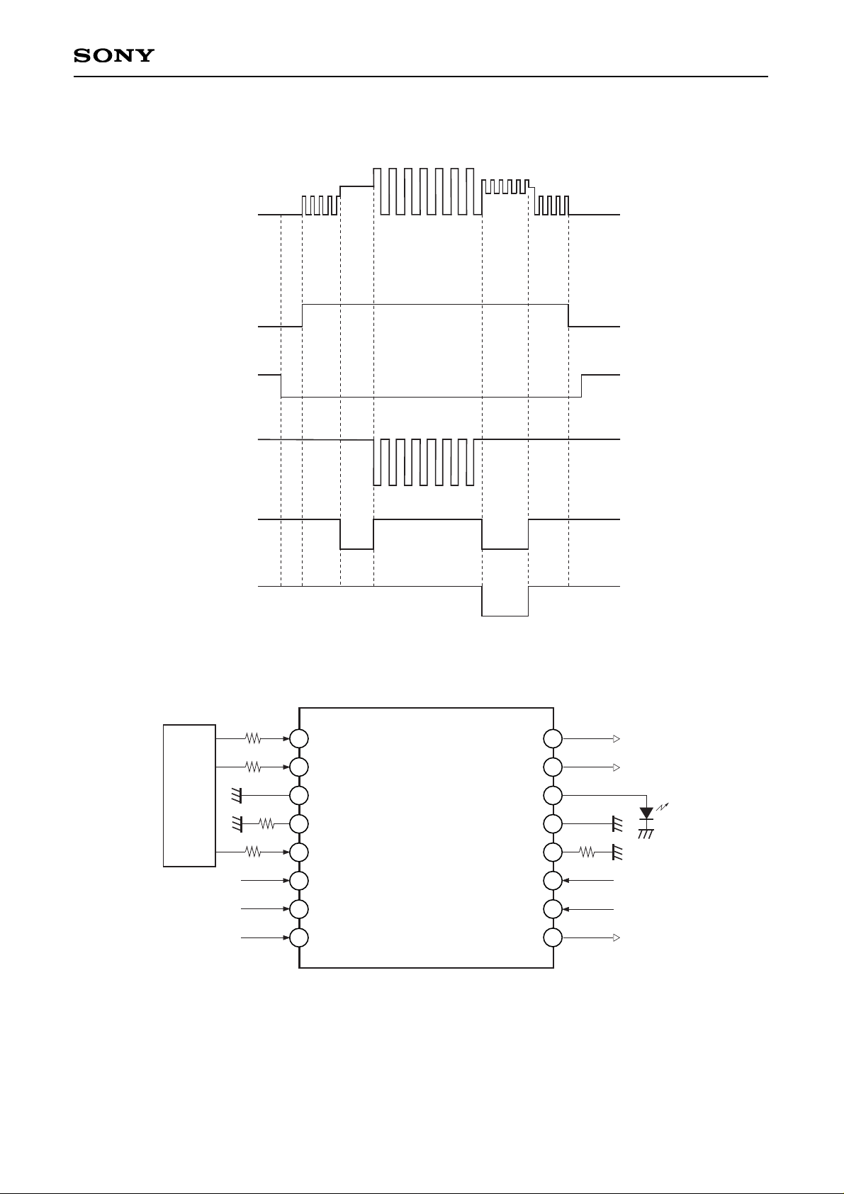
Be sure to also check the timing chart on page 7.
Oscillator OFF
IINR input current [µA]
IR – Output current [mA]
0
Initial setting
IO – Oscillator amplitude [mAp-p]
OSCGA external resistance [Ω]
12 2k
IO + 2 (IR – IO)
For large OSCGA
external resistance
(Io ≈ 0mA)
For small OSCGA
external resistance
2I
R
IR
IINR input current [µA]
Level adjustment
Oscillator amplitude [mAp-p]
IR < IO IR > IO
IO
IO
IO ≈ × [mAp-p]
OSCGA pin voltage
OSCGA external resistance
40
9
Page 6
– 6 –
CXA2610N
Notes on Operation
• Locate the external resistors connected to the IINR, IIN2 and IIN3 pins close to the IC package to prevent the
effect from other signal lines.
• Make the wiring distance between the output LD0 pin and the laser diode as short as possible.
If this wiring is longer, the output waveform characteristics show that the rise and fall times (Tr and Tf)
become slower as the ringing becomes larger.
• The external resistor connected to Pin 10 (OSCGA) should be within the range from 12Ω to 2kΩ.
In addition, this resistance value should be set in consideration of the laser diode Ith so that the oscillation
level at IINR = 0V does not exceed the read power.
• Temperature assurance
The junction temperature for the CXA2610N laser driver should not exceed 150°C. In addition, the power
consumption (PO) should be the allowable power dissipation (PD) or less, and the IC should be used with a
lowered thermal resistance (θj-a) for board mounting so that normal operation is possible at the maximum
operating temperature of 70°C.
Widening the GND area on the set board and other heat radiation countermeasures within the set are
necessary in order to lower θj-a.
This is because the CXA2610N thermal resistance (θj-a) differs according to the board, and the power
consumption (PO) is also difficult to predict with future increases in power.
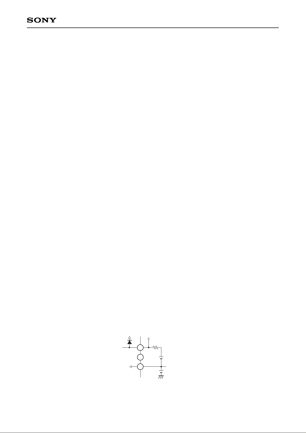
Obtain the thermal resistance (θj-a) and power consumption (PO) of the package by the following method.
Power consumption (PO): Oscillator ON state (OSC level = 47mAp-p)
PO = (ICC2 + (total of each input current × 10)) × VCC + (IOP × (VCC – VOP))
ICC2: See page 3 of this Data Sheet.
IOP: Output drive current flowing from the LD0 pin to the laser diode
VOP: Laser diode operating voltage
or, the power consumption can also be obtained as follows.
PO = (ICC × VCC) – (IOP × VOP)
ICC: Device current consumption (including IOP) during operation
Thermal resistance (θj-a) when mounted on a board
The diode temperature coefficient is –2.27mV/°C
(1) ENABLE pin voltage – VCC pin voltage after applying 0V to the IINR, IIN2 and IIN3 pins = V1
(2) ENABLE pin voltage – VCC pin voltage immediately after applying 3V to IINR = V2
(3) ENABLE pin voltage – VCC pin voltage after applying 3V to the IINR pin and reaching a
thermally balanced state = V3
The change in current consumption between (1) and (2) ∆ICC = (3V/(Rext + 250Ω)) × 104.
This ∆ICC causes the ENABLE pin internal forward protective diode connection VCC voltage to vary
(∆VCC) due to the effects of the wiring resistance from the VCC pin voltage which is used as the
reference.
The voltage fall coefficient (VR) used to correct this ∆VCC can be obtained by VR = (V1 – V2)/∆ICC.
Using VR to apply correction to V3 yields the equation:
(∆ICC × VR) + V3 = V4.
From this, ∆Tj = (V4 – V2) mV/–2.27mV/°C, and θj-a = ∆Tj/PO [°C/W].
• Allowable power dissipation (PD) ≥ PO [W]
PD = (150°C – ambient temperature)/θj-a
• Maximum operating temperature 70 °C
(150°C – ∆Tj) ≥ 70°C
Thus, if θj-a can be lowered from these two conditions, the maximum operating temperature can also
be raised.
10
11
5V
5V
5V
10V
1MΩ
Diode measurement point
ENABLE
V
CC
VCC
9
Thermal Resistance Measurement Circuit
Page 7
– 7 –
CXA2610N
Timing Chart
LD0
ENABLE
CONTR
CONT2
CONT3
OSCENA
Application Circuit
TTL/CMOS
LD
TTL/CMOS
1
2
3
4
5
6
7
8
9
10
11
12
13
14
15
16
Vcc
Vcc
LD0
GND
OSCGA
ENABLE
OSCENA
Vcc
IINR
IIN2
GND
OSCFR
IIN3
CONTR
CONT2
CONT3
TTL/CMOS
TTL/CMOS
TTL/CMOS
Voltage
DAC
Application circuits shown are typical examples illustrating the operation of the devices. Sony cannot assume responsibility for
any problems arising out of the use of these circuits or for any infringement of third party patent and other right due to same.
Page 8

– 8 –
CXA2610N
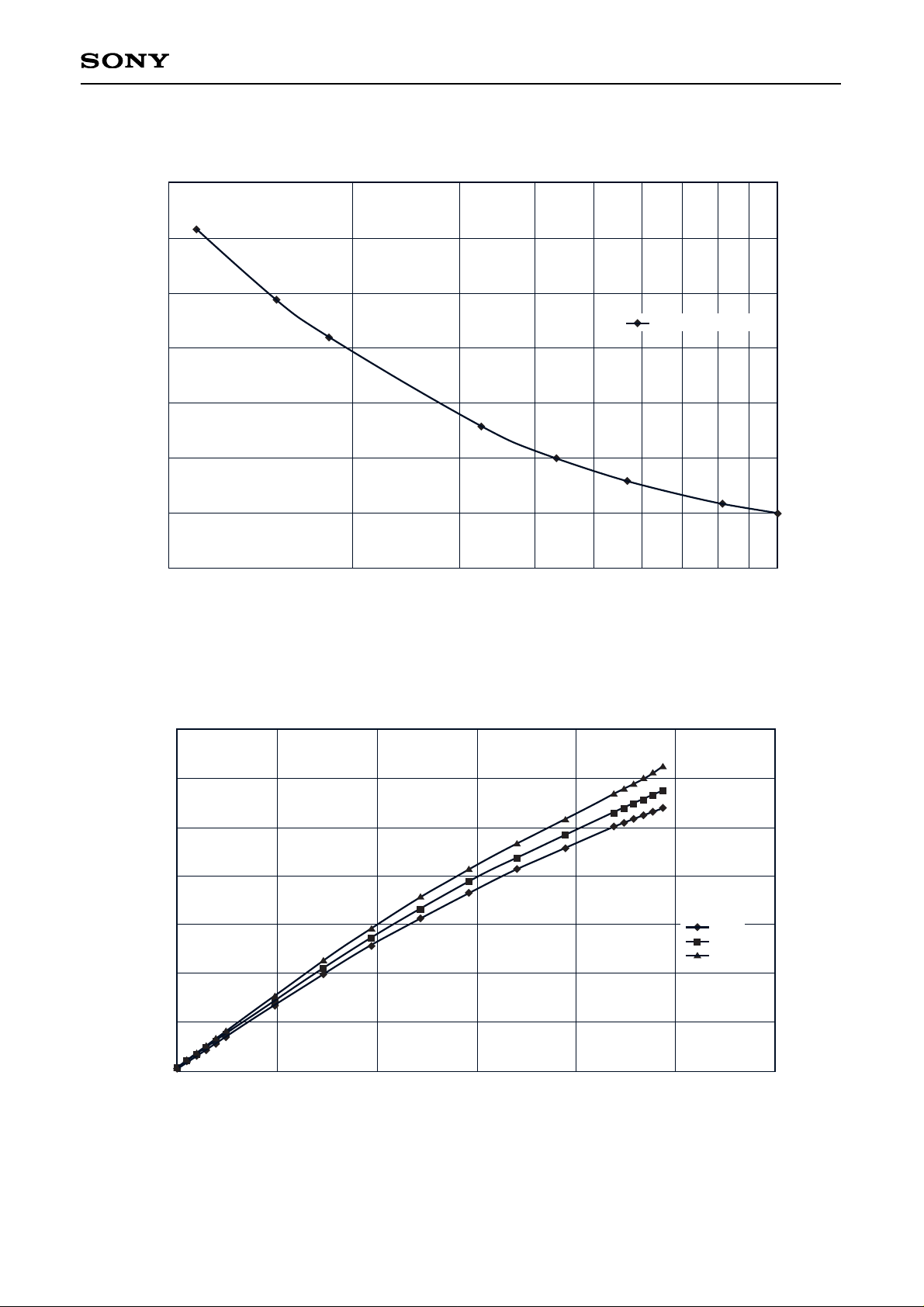
Example of Representative Characteristics
0
0
50
Oscillator amplitude [mAp-p]
IINR input current [µA]
High frequency oscillator amplitude vs. Read current characteristics
100
150
200
250
200 400 600 800 1000 1200 1400
0
0
40
60
20
Oscillator amplitude [mAp-p]
IINR input current [µA]
High frequency oscillator amplitude frequency dependence (OSCGA = 20Ω)
80
100
120
140
160
180
200
200 400 600 800 1000 1200 1400
20Ω
2kΩ
OSCGA external resistance value
Approximately 200MHz
Approximately 400MHz
Page 9
– 9 –
CXA2610N
1
0
300
200
100
Oscillator frequency [MHz]
OSCFR pin external resistance value [kΩ]
High frequency oscillator frequency vs. External resistance
400
500
600
700
10
0
0
Output current [mA]
Input current [µA]
IIN3 input/output current characteristics
50
100
150
200
250
300
350
500 1000 1500 2000 2500 3000
Oscillator frequency
Supply voltage
5V
4.5V
5.5V
Page 10

– 10 –
CXA2610N
Package Outline Unit: mm
16PIN SSOP (PLASTIC)
SONY CODE
EIAJ CODE
JEDEC CODE
PACKAGE STRUCTURE
PACKAGE MATERIAL
LEAD TREATMENT
LEAD MATERIAL
PACKAGE MASS
EPOXY RESIN
SOLDER / PALLADIUM
42/COPPER ALLOY
0.1g
SSOP-16P-L01
SSOP016-P-0044
b=0.22 – 0.05
+ 0.1
0.15 – 0.02
+ 0.05
PLATING
0.1 ± 0.1
0.5 ± 0.2
0° to 10°
DETAIL A
NOTE: Dimension “∗” does not include mold protrusion.
∗5.0 ± 0.1
0.65
8
1
9
16
∗4.4 ± 0.1
6.4 ± 0.2
1.25 – 0.1
+ 0.2
A
0.1
0.13
M
B
b
(0.22)
(0.15)
0.15 – 0.01
DETAIL B : SOLDER DETAIL B : PALLADIUM
+ 0.03
b=0.22 ± 0.03
NOTE : PALLADIUM PLATING
This product uses S-PdPPF (Sony Spec.-Palladium Pre-Plated Lead Frame).
 Loading...