

Page 1

—1—
E97X12-TE
Sony reserves the right to change products and specifications without prior notice. This information does not convey any license by
any implication or otherwise under any patents or other right. Application circuits shown, if any, are typical examples illustrating the
operation of the devices. Sony cannot assume responsibility for any problems arising out of the use of these circuits.
Absolute Maximum Ratings (Ta=25 °C)
• Supply voltage VCC 12 V
• Operating temperature Topr –20 to +75 °C
• Storage temperature Tstg –65 to +150 °C
• Allowable power dissipation
PD 650 mW
Operating Conditions
Supply voltage VCC—VEE 4.5 to 5.5 V
Description
The CXA2568M is an IC developed for compact
disc players. This IC incorporates an RF amplifier,
focus error amplifier, tracking error amplifier, APC
circuit and RF level control circuit. (The voltageconverted optical pickup output is supported.)
Features
• Low power consumption (50 mW at ±2.5 V)
• High-band RF amplifier
• APC circuit
• RF level control circuit (Hold circuit included)
• Both single power supply and dual power supply
operations possible.
• Compatible with pickup for LC and PD
Applications
Compact disc players
Structure
Bipolar silicon monolithic IC
RF Amplifier for CD Players
24 pin SOP (Plastic)
CXA2568M
Page 2

—2—
CXA2568M
Block Diagram and Pin Configuration
V
CC
1k
56k
10k
56k
10k
V
CC
55k
10k
VREF
1.25V
V
EE
APC LD AMP
V
EE
10k
V
CC
13.4k
VC
50µA
44.1k
24k
23.3k
24k
23.3k
24k
23.3k
V
EE
5.7k
25.4k
VEE
VC
5k14k
VC
RF SUMMING AMP RF_EQ_AMP
174k
VC
174k
25p
ERROR AMP
FPCUS
25p
820k
VC
12p
260k
R34
147
VC
R26
15k
30k
V
EE
VCC
158.45k23.8k
158.45k
VC
TRACKING
ERROR AMP
23.8k
VC BUFFER
670mV
V
CC
LC/PD
LD_ON
AGCCONT
HOLD_SW
RF_BOT
RFTC
RF_I
RFO
RFE
FE
TE
(60%/40%/OFF)
HOLD
AGCVTH
LD
PD
A
B
C
D
V
EE
F
E
VC
30k
13k
26k
VC
VC
260k 26k
VC
13k
12p
820k
24k
23.3k
VC
20k
100k
15k
100k
APC PD AMP
22
21
20
19
18
17
16
15
14
23
13
24
7
8
9
1
2
3
4
6
10
12
11
5
15k
Page 3
—3—
CXA2568M
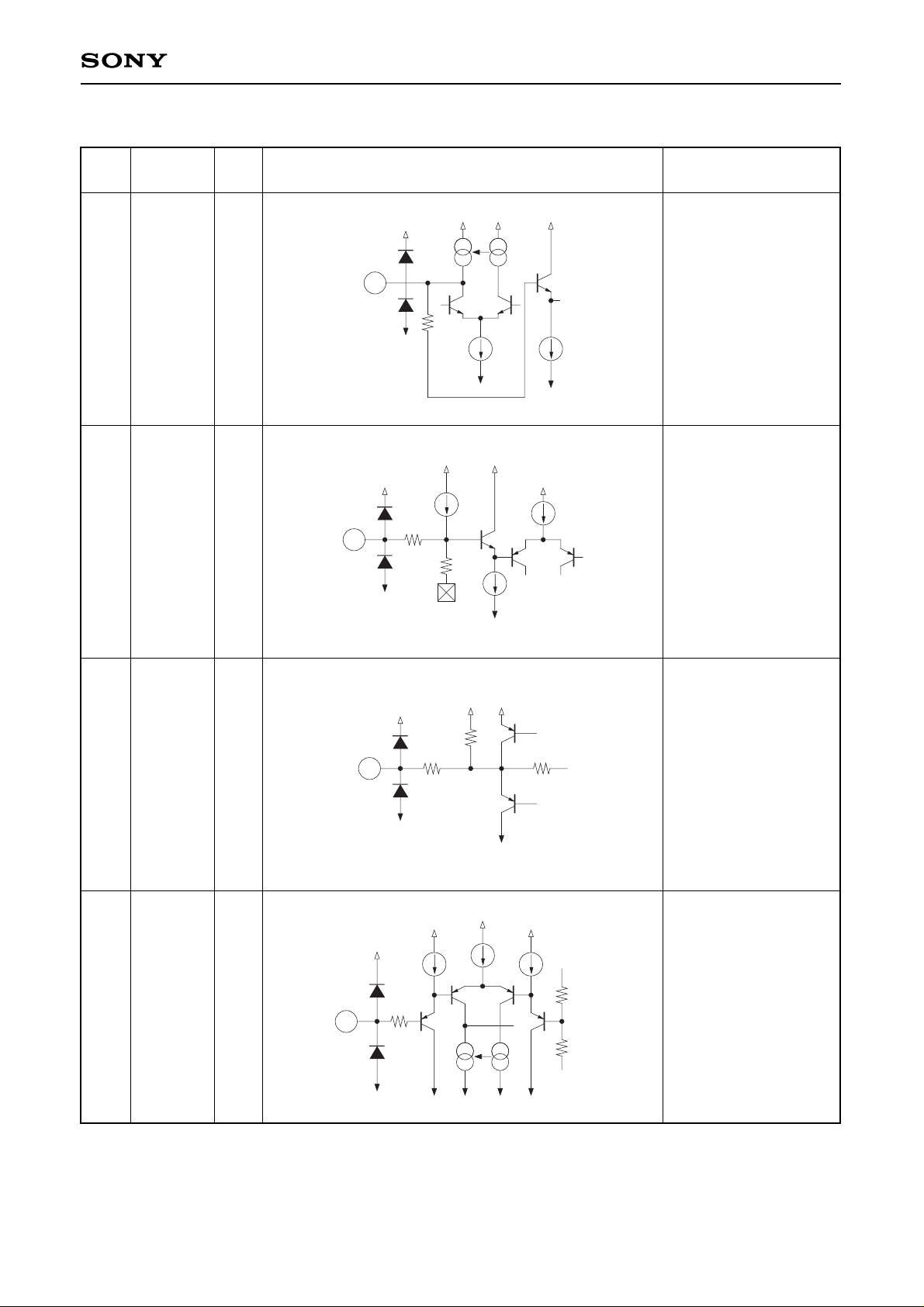
Pin Description
Pin
Symbol IO Equivalent circuit Description
No.
1
2
3
4
HOLD
AGCVTH
LD
PD
—
—
O
I
External hold timeconstant pin for RF
level control.
Variable pin of
reference level for RF
level control.
The reference level can
be varied by the
external resistor.
Output pin of APC
amplifier.
Input pin of APC
amplifier.
1k
10k
55.7k
V
CC VCC
VEE
3
147
50µ
10µ
13.4k
2
147
500µ
VEE
1
147
55k
10k
17µ
V
CC
VEE VEE VEE VEE
4
Page 4
—4—
CXA2568M
Pin
Symbol IO Equivalent circuit Description
No.
5
6
7
8
9
10
11
23
12
A
B
C
D
VEE
TE
E
LC/PD
VC
I
I
I
I
—
I
I
I
O
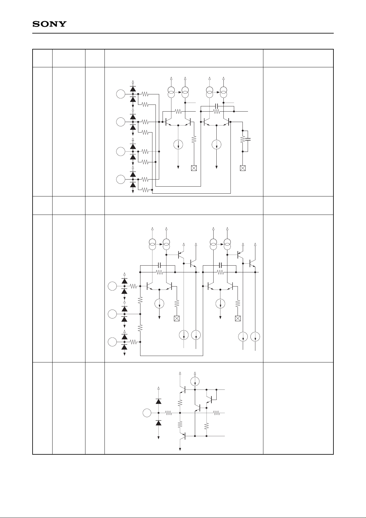
Input pin of RF and FE
amplifiers for Pins 5, 6,
7 and 8.
VEE.
Input pin of tracking
error amplifier for Pins
10 and 11.
An external resistor for
V-I conversion should
be connected because
these pins are for
current input.
Pin 23 is a bias for LC
when connected to VCC
and for PD IC when left
open.
DC voltage output pin of
(VCC+VEE)/2.
Connect to GND when
dual power supply (±2.5
V) is used; connect a
smoothing capacitor
when single power
supply (+5 V) is used.
A
24k
23.2k
B
24k
23.2k
C
24k
23.2k
D
24k
23.2k
14k
100µ
VC
4.2k
VEE
8µ
VEE
VCC VCC VCC VCC
174k
25p
VC
174k
25p
5
6
7
8
147
147
23
820k
820k
8µ
V
EE
VCC VCC
403k
12p
96.3k
VC
8µ
V
EE
96.3k
VC
VCC VCC
12p
VCC VCC
10
VCC VCC
11
403k
12
147
120
120
VCC
VEE
VCC
16k
15k
200µ
Page 5
—5—
CXA2568M
Pin
Symbol IO Equivalent circuit Description
No.
13
14
15
16
17
TE
FE
REF
RFO
RF_I
O
O
—
O
I
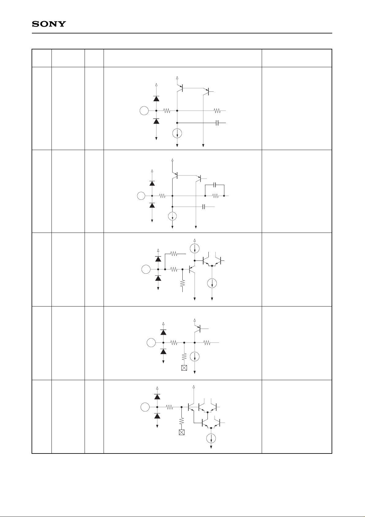
Output pin of tracking
error amplifier.
The F-E signal is
output.
Output pin of focus
error amplifier.
Equalizing pin of RF
amplifier.
Frequency response
can be adjusted by
connecting CR to this
pin.
Output pin of RF
amplifier.
Input pin of RF amplifier
output RFO with
capacitance coupled.
13
147 158.45k
10p
400µ
VEE VEE
VCC
147
400µ
VCC
VEE VEE
10p
174k
25p
14
5.7k
5k
25.4k
25µ
15
147
VCC
800µ
25.4k
60k
16
147
15k
20µ
17
Page 6
—6—
CXA2568M
Pin
Symbol IO Equivalent circuit Description
No.
18
19
20
21
22
24
RFTC
RF_BOT
AGCCONT
HOLD_SW
LD ON
VCC
—
—
I
I
I
—
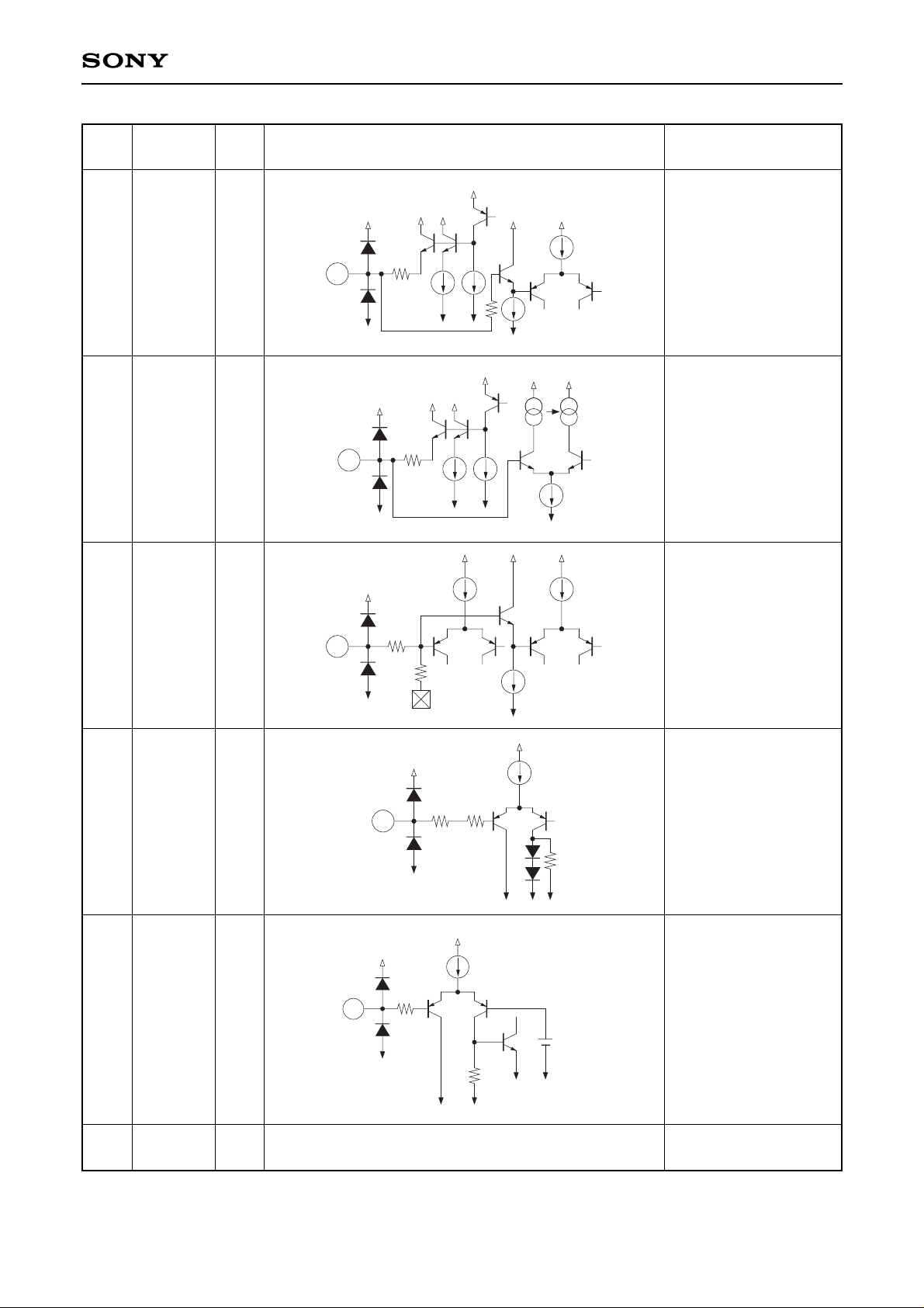
External time-constant
pin for RF level control.
External bottom timeconstant pin for RF
level control.
RF level control ON
(limit level of 60 % / 40
%)/ OFF switching pin.
60 % for VCC, 40 % for
open or VC and OFF for
VEE.
RF level control hold
ON/OFF switching pin.
ON for VCC and OFF for
VEE.
ON/OFF switching pin
of APC amplifier.
ON for VCC and OFF for
VEE.
VCC
147
50µ
10µ
50µ
18
147
50µ
50µ
19
20µ
147
15µ
7µ
50k
15µ
20
147
21
22
147
50µ
VEE VEE
30k
VEE VEE
VREF
V
CC
Page 7
—7—
CXA2568M
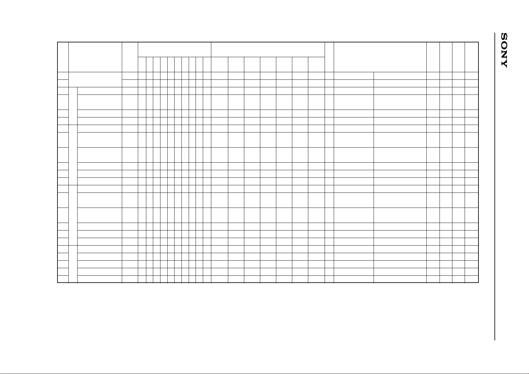
Electrical Characteristics ±2.5 V power supply (VCC=2.5 V, VEE=–2.5 V, VC=GND)
1
2
3
4
5
6
7
8
9
10
11
12
13
14
15
16
17
18
19
20
21
22
23
Measurement item
Current consumption
Offset voltage 1
Voltage gain
Maximum output amplitude H
Maximum output amplitude L
Offset voltage
Voltage gain 1
Voltage gain 2
Voltage gain difference
Maximum output amplitude L
Maximum output amplitude H
Offset voltage 1
Voltage gain 1
Voltage gain 2
Voltage gain difference
Maximum output amplitude H
Maximum output amplitude L
Output voltage 1
Output voltage 2
Output voltage 3
Output voltage 4
Maximum output amplitude
Symbol
I
CC
IEE
V16-1
V16-2
V16-3
V16-4
V14-1
V14-2
V14-3
V14-4
V14-5
V14-6
V13-1
V13-2
V13-3
V13-4
V13-5
V13-6
V3-1
V3-2
V3-3
V3-4
V3-5
SW conditions
12345678910
OOOO
OOOO O
OOOO O
OO
OO
OO O
OO O
O
O
OO
OO
O
Bias conditions
E1 E2 E3 E4 AC1 AC2 I1
1 kHz
100 mVp-p
280 mV
–280 mV
1 kHz
100 mVp-p
1 kHz
100 mVp-p
310 mV
310 mV
1 kHz
140 mVp-p
1 kHz
140 mVp-p
270 mV
270 mV
2.0 V 1.3 V 230 µA
2.0 V 1.3 V 410 µA
2.0 V 1.3 V 590 µA
0.5 V 1.3 V 0 µA
2.0 V 1.3 V 0 µA
24
9
16
16
16
16
14
14
14
14
14
14
13
13
13
13
13
13
3
3
3
3
3
Description of I/O waveform
and
measurement method
Input GND
Input GND
Input GND Output DC measurement
Output AC measurement
Output DC measurement
Output DC measurement
Input GND Output DC measurement
Output AC measurement
Output AC measurement
V15-4=V15-2–V15-3
Output DC measurement
Output DC measurement
Input GND Output DC measurement
Output AC measurement
Output AC measurement
V13-4=V13-2–V13-3
Output DC measurement
Output DC measurement
Output DC measurement
Output DC measurement
Output DC measurement
LD OFF Output DC measurement
I2=0.8 mA Output DC measurement
Min. Typ. Max. Unit
6.5 10 13.5 mA
–13.5 –10 –6.5 mA
–25 0 25 mV
19.9 22.9 25.9 dB
2.2 — — V
——–2V
–30.0 0 30.0 mV
20.3 23.3 26.3 dB
20.3 23.3 26.3 dB
–3.0 0 3.0 dB
— –1.9 V
1.9 — V
–35 0 35 mV
21.9 24.9 27.9 dB
21.9 24.9 27.9 dB
–3.0 0 3.0 dB
1.9 — — V
— — –1.9 V
— –1.7 –0.3 V
–1.5 0 1.1 V
0.6 2.0 — V
2.1 2.3 — V
—— 0 V
RF amplifierFE amplifierTE amplifierAPC
∗ O in the SW conditions represents the ON state.
Measurement No.
Measurement pin
Page 8
—8—
CXA2568M
24
25
26
27
28
29
30
31
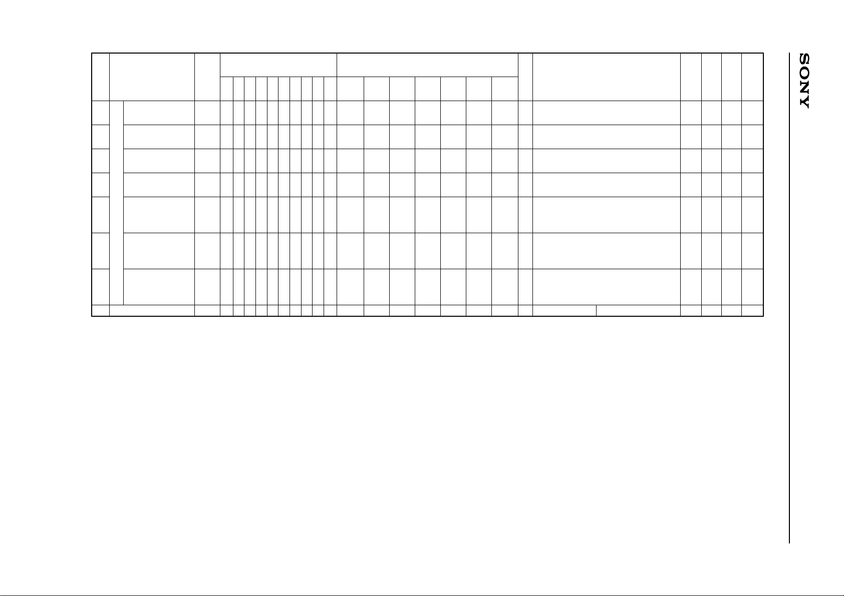
Measurement item
60 % limit
40 % limit
–60 % limit
–40 % limit
Hold characteristics
Response
characteristics 1
Response
characteristics 2
Center output voltage
Symbol
V3-6
V3-7
V3-8
V3-9
V1-1
V1-2
V1-3
V12-1
SW conditions
12345678910
OOOO O
OOOO O
O
O
Bias conditions
E1 E2 E3 E4 AC1 AC2 I1
50 mV 2.0 V
3.8 V/1.3 V
700 µA
50 mV 2.0 V
3.3 V/1.3 V
700 µA
2.0 V
3.8 V/1.3 V
100 kHz
170 µA
1.6 Vp-p
2.0 V
1.8 V/1.3 V
100 kHz
170 µA
1.6 Vp-p
4 V/1 V
3.8 V/1.3 V
1 V
3.8 V/1.3 V
1 V
3.8 V/1.3 V
3
3
3
3
1
1
1
12
Description of I/O waveform
and
measurement method
Level control : 60 % (E4 : 4 V)
–Level control OFF (E4 : 0.5 V)
Level control : 40 % (E4 : 2.5 V)
–Level control OFF (E4 : 0.5 V)
Level control : –60 % (E4 : 4 V)
–Level control OFF (E4 : 0.5 V)
Level control : –40 % (E4 : 2.5 V)
–Level control OFF (E4 : 0.5 V)
HOLD OFF → ON (t=0 ms)
Level control 60 % → OFF (t=10 ms)
V (t=100 ms)–V (t=0 ms)
HOLD OFF Level control 60 %
→ OFF (t=0 ms)
(V (t=1 ms)–V (t=0 ms))/(steady value–V (t=0 ms))
HOLD OFF Level control OFF
→ 60 % (t=0 ms)
(V (t=1 ms)–V (t=0 ms))/(steady value–V (t=0 ms))
Output DC measurement
Min. Typ. Max. Unit
–2950–2350–1150 mV
–1620–1120 –120 mV
1550 2350 2800 mV
598 1098 1598 mV
–10 –2 0 mV
98 — 100 %
98 — 100 %
–100 — 100 mV
RF level control
∗ O in the SW conditions represents the ON state.
Measurement No.
Measurement pin
Page 9
—9—
CXA2568M
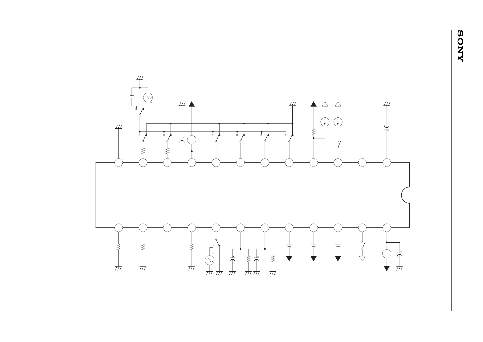
Electrical Characteristics Measurement Circuit
HOLD
AGCVTH
LD
PD
A
B
C
D
V
EE
F
E
VC
V
CC
LC/PD
LD_ON
HOLD_SW
AGCCONT
RF_BOT
RF TC
RF_I
RFO
REF
FE
TE
VEEAGND
VCC
S9
VEE
E2
VEE
E3
C1
33µ
GND GND
R1
1M
C3
0.01µ
S10
GNDGND
AC2
GND
R3
10k
GND
R8
10k
GND
R9
10k
S8
0.8mA
I2
VCC VCC VEE
I1
R1
300
GND
S1
S2
S3
S4
VEE
A
C4
33µ
GND
R2
150k
S5
R4
150k
S6
S7
AC1 E1
GND
GND
VEE
E4
GND GND
R1
1M
C3
0.01µ
GND
C3
0.33µ
7 8 91 2 3 4 5 6 10 11 12
22 21 20 19 18 17 16 15 1423 1324
Page 10
—10—
CXA2568M
Description of Functions
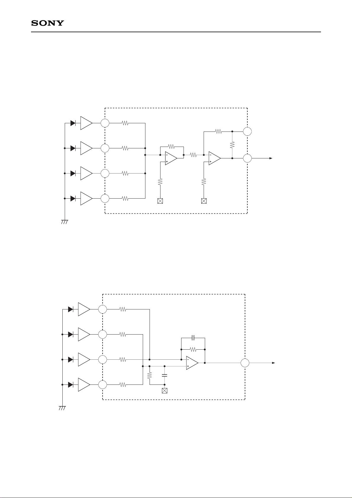
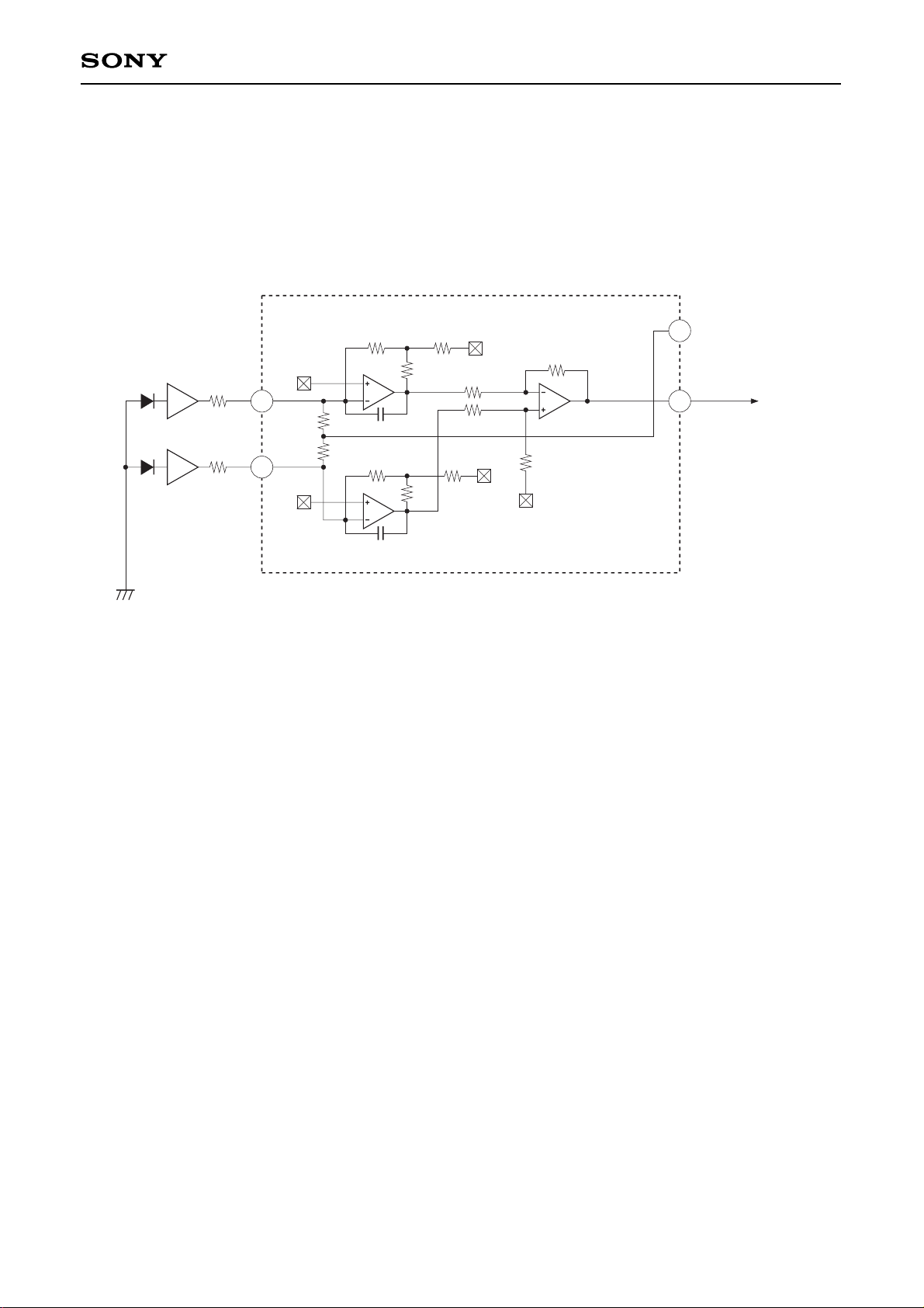
RF Amplifier
Each signal current from the photodiodes A, B, C and D is I-V converted, and input to Pins 5, 6, 7 and 8.
These signals are added by the RF summing amplifier and equalized by the RF equalizing amplifier and then
output to Pin 16. When the RF signal is equalized, an equalizing circuit is added to Pin 15.
Focus Error Amplifier
The operation of (B+D)–(A+C) is performed and the signal is output to Pin 14.
I-V
A
A
24k
I-V
B
B
24k
I-V
C
C
24k
I-V
D
D
24k
GND
14k
4.2k
VC
4.3k
5k
RF SUMMING AMP
5.7k
VC
25.4k
RF EQAMP
RFOUT
REF
RFO
5
6
7
8
15
16
GND
VC
FEOUT
FE
I-V
A
A
I-V
B
B
I-V
C
C
I-V
D
D
23.3k
23.3k
23.3k
23.3k
174k
25p
174k
25p
FOCUS
ERROR AMP
14
V
CC
5
6
7
8
Page 11
—11—
CXA2568M
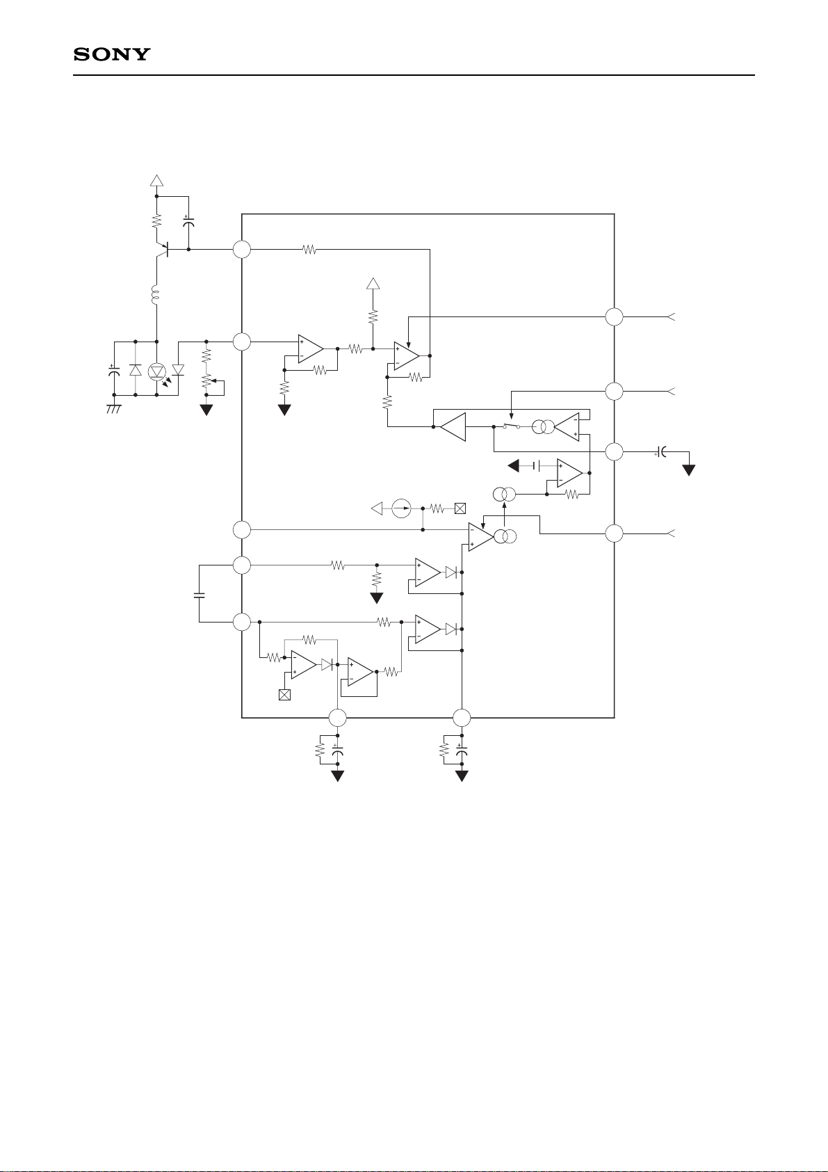
Tracking Error Amplifier
Each signal current from the photodiodes E and F is I-V converted and input to Pins 10 and 11 via an input
resistor which determines the gain. The signal is amplified by the gain amplifier, operated by the tracking error
amplifier and then the (F-E) signal is output to Pin 13.
Pin 23 can be used as a bias for LC when connected to VCC and as a bias for PD IC when left open.
GND
TEOUT
TE
I-V
F
I-V
E
150k
150k
12p
TRACKING
ERROR AMP
158.45k
820k
260k
13k
26k
VC
VC
23.8k
23.8k
820k
VC
158.45k
12p
VC
LC/PD
23
1310
11
VC
26k
13k
260k
Page 12
—12—
CXA2568M
C3
100µ
VCC
R1
22
L1
10µH
GND VEE
LD PD
PD
LD
R3
100
R2
500
C1
1µ
VEE
R7
55k
R5
10k
R6
1k
R16
56k
VCC
R17
56k
R15
10k
VEE
Vhold
R20
12.5k
22
LD ON
AGCCONT
MICRO
COMPUTER
MICRO
COMPUTER
VEE
RF_I
RFO
C2
0.01µ
3
4
R14
10k
×1
VEE
VL
VREF
1.25V
HOLD_SW
MICRO
COMPUTER
21
2
R10
20k
V
EE
R11
44.1k
R12
100k
16
17
1
HOLD
C6
10µ
20
V2
R18
13.4k
50µA
V
CC
R13
100k
670mV
R4
15k
R6
15k
V1
19
R9
1M
C4
0.1µ
RF_BOT
VEE
RFTC
18
R19
1M
AGCVTH
C5
1µ
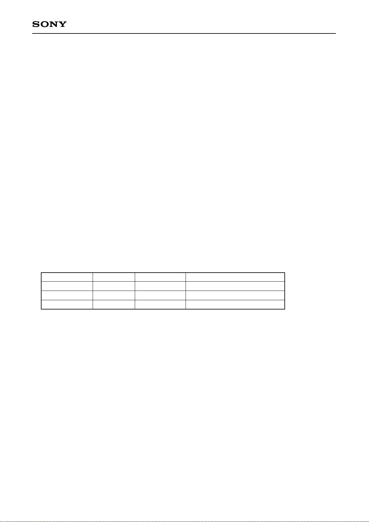
APC & Laser Power Control
Page 13
—13—
CXA2568M
• APC
When the laser diode is driven by a constant current, the optical power output has extremely large negative
temperature characteristics.
The APC circuit is used to maintain the optical power output at a constant level.
The laser diode current is controlled according to the monitor photodiode output.
APC is set to ON by connecting the LD ON pin to VCC ; OFF by connecting it to VEE.
• Laser Power Control (LPC)
The RF level is stabilized by attaching an offset to the APC VL and controlling the laser power in sync with
the RF level fluctuations.
The RFO and RF_I levels are compared and the larger of the two is smoothed by the RFTC’s external CR.
This signal is then compared with the reference level.
The laser power is controlled by attaching an offset to VL according to the results of comparison with the
reference level.
Set the reference level to 670 mV. (center voltage reference)
When the reference level is changed, connect the external resistor to the AGCVTH pin (Pin 2). The
reference level can be lowered by connecting the resistor between Pin 2 and the center output voltage or
between Pin 2 and VCC.
The AGCCONT pin (Pin 20) is used to switch the level of the laser power control circuit ; OFF, ON (laser
power limit of 40 %) and ON (laser power limit of 60 %).
The HOLD_SW pin (Pin 21) is used to switch the hold ON and OFF for the VL signal. Set this pin to ON so
as not to follow the fluctuation of the RF signal.
AGCCONT
L (VEE)
M (VC or OPEN)
H (VCC)
LPC
OFF
ON
ON
LPC limit
—
40 %
60 %
VL variable range
Approximately 1.27 V
Approximately 1.27 V±350 mV
Approximately 1.27 V±570 mV
Page 14
—14—
CXA2568M
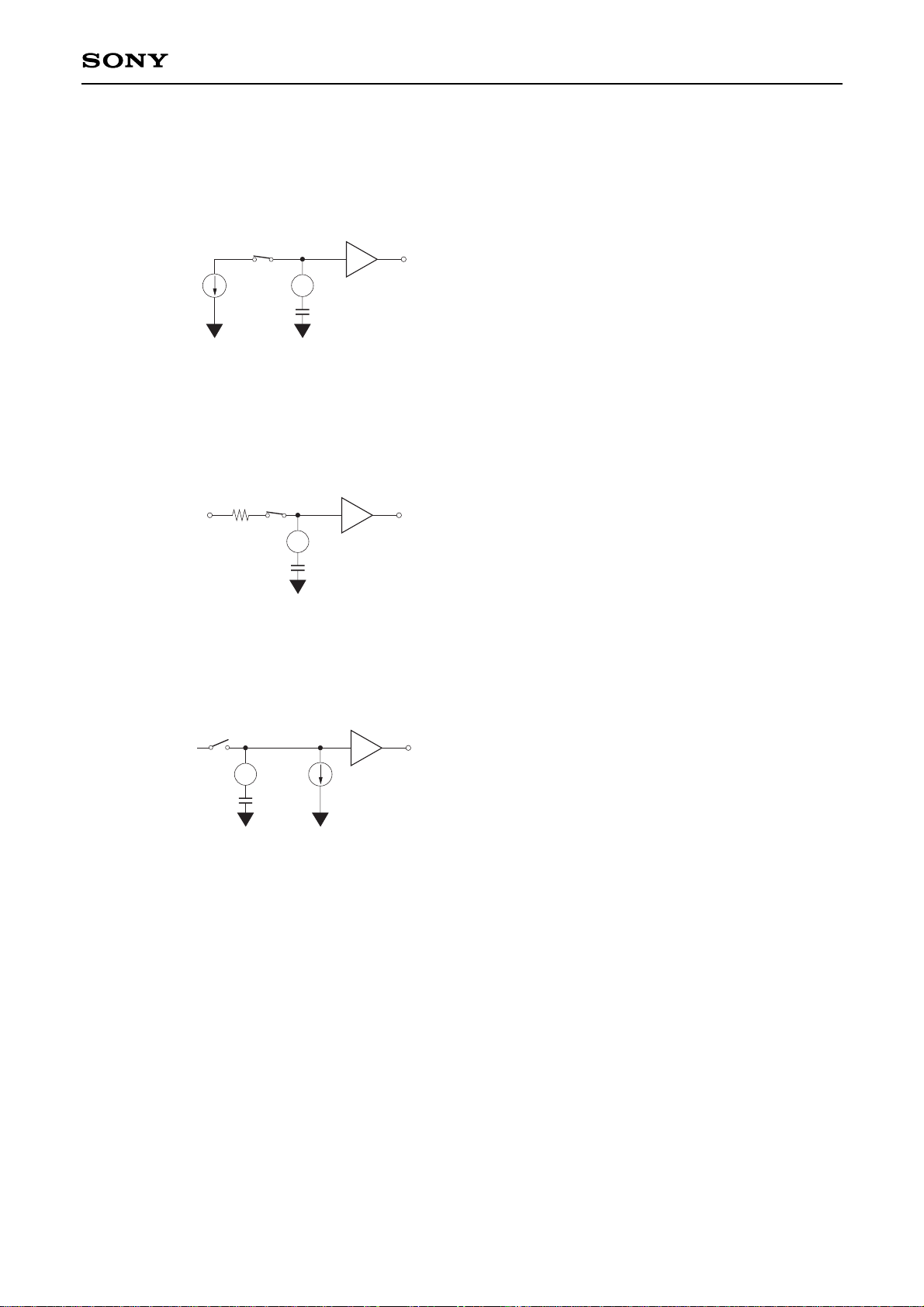
The hold ON/OFF operation is approximately as follows.
1. HOLD : Operation for OFF
(a) | VL–Vhold | ≥2VT (VT≈26 mV)
(typ.) Ic=500 µA (VL<Vhold)
–500 µA (VL>Vhold)
(b) | VL–Vhold | <2VT
(typ.) R=105 Ω
2. HOLD : Operation for ON
(typ.) Ib=6.5 nA
VEE
Vhold
×1
VL
VEE
21
HOLD
C
IC
Vhold
×1
VL
VEE
21
HOLD
C
R
Vhold
×1
VEE
21
HOLD
C
VEE
IB
Page 15
—15—
CXA2568M
Center Voltage Generation Circuit
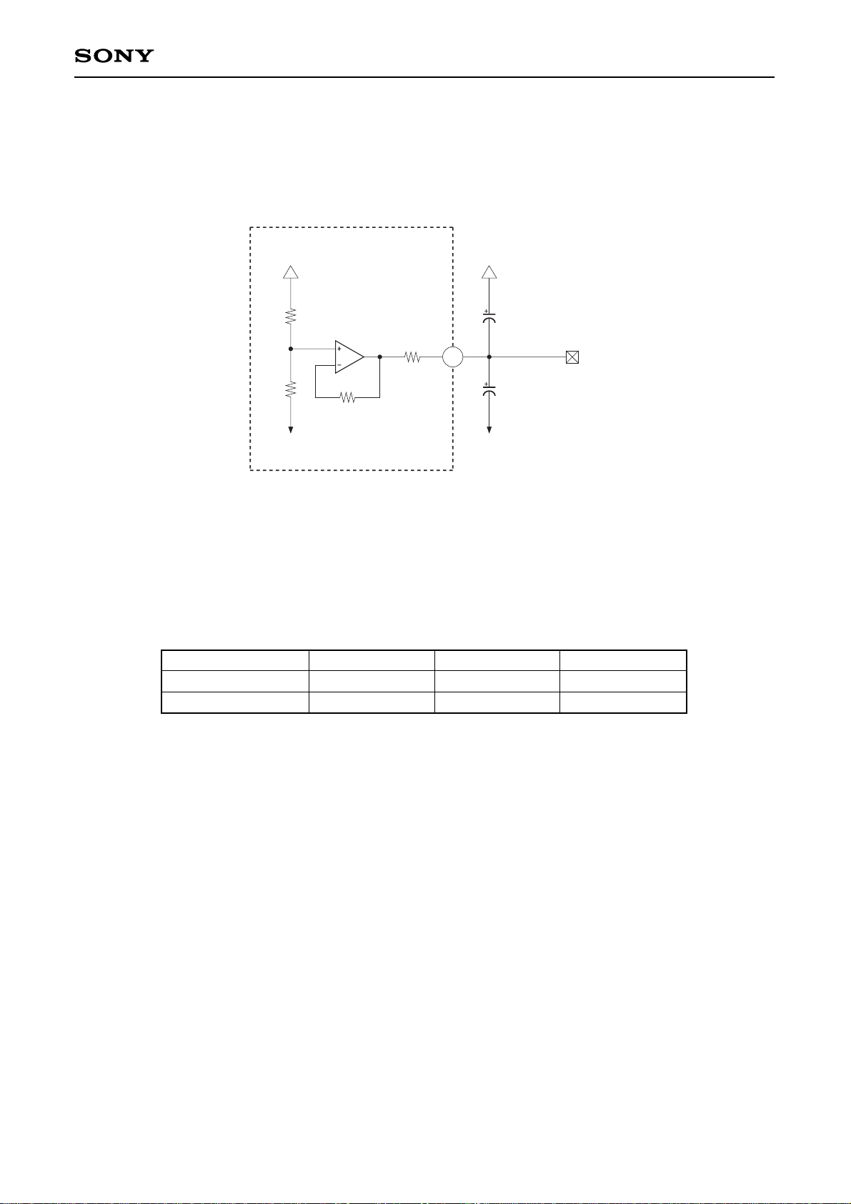
This circuit provides the center potential when this IC is used at single power supply. The maximum current
is approximately ±3 mA. The output impedance is approximately 147 Ω. Connect this circuit to GND when
used at dual power supply.
Notes on Operation
1. Power supply
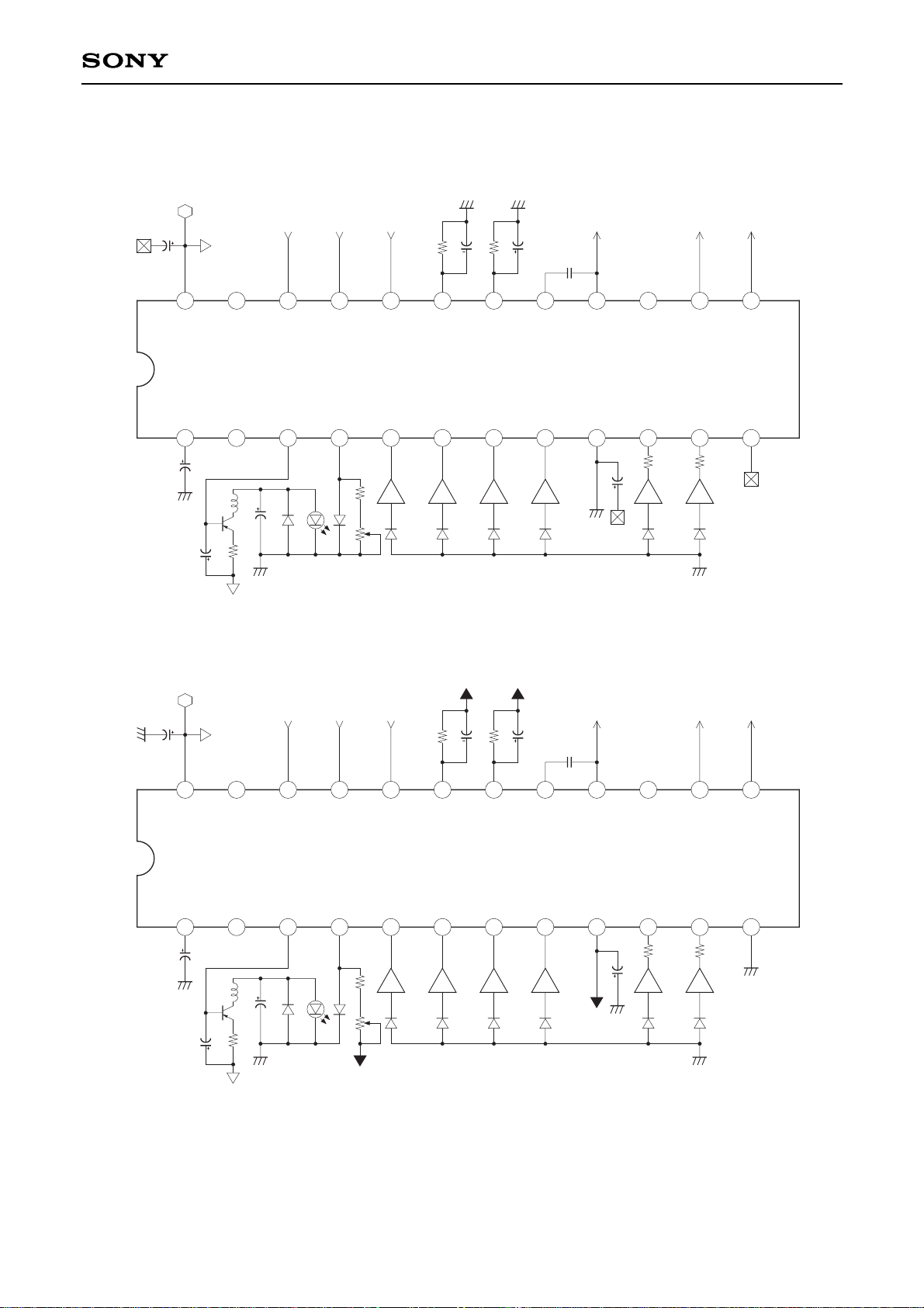
The CXA2568M can be used either at dual power supply or single power supply. The table below shows
the connection of power supply for each case.
2. Laser power control
The RF level is stabilized by attaching an offset to the APC VL and controlling the laser power in sync with
the RF level fluctuations. Therefore, use this circuit in the state where the focus servo is applied.
The laser life is shortened by increasing the laser power when the less light is reflected from the disc. It is
recommended that the typical laser power value is set lower to maintain the laser life.
The laser power limit value depends on the external circuit. Select the laser power limit setting considering
the external conditions.
Take care of the laser maximum ratings when using the laser power control circuit.
30k
30k
VCC
VEE
12
15k
147
VC BUFFER
VCC
VEE
33µ/6.3V
33µ/6.3V
VC
VC
Dual power supply
Single power supply
VCC
+power supply
Power supply
VEE
–power supply
GND
VC
GND
OPEN
Page 16
—16—
CXA2568M
Application Circuit
• For single power supply +5 V
• For dual power supply +2.5 V
HOLD
AGCVTH
LD
PD
A
B
C
D
V
EE
F
E
VC
GND
GND
10µ
V
CC
LC/PD
LD_ON
HOLD_SW
AGCCONT
RF_BOT
RF TC
RF_I
RFO
REF
FE
TE
(60%/40%/OFF)
33µ/6.3V
VC
V
CC
MICRO
COMPUTER
MICRO
COMPUTER
MICRO
COMPUTER
1MEG
0.1µ
GND
0.01µ
SSP
SSP
SSP
22 21 20 19 18 17 16 15 1423 1324
100
500
1µ/6.3V
GND
I_V
A
I_V
B
I_V
C
I_V
D
VC
I_V
F
33µ/6.3V
150k
I_V
E
GND
VC
7 8 91 2 3 4 5 6 10 11 12
22
10µH
100µ/6.3V
VCC
LD
PD
150k
1MEG
1µ
+5V
HOLD
AGCVTH
LD
PD
A
B
C
D
V
EE
F
E
VC
GND
10µ
V
CC
LC/PD
LD_ON
HOLD_SW
AGCCONT
RF_BOT
RF TC
RF_I
RFO
REF
FE
TE
(60%/40%/OFF)
33µ/6.3V
V
CC
MICRO
COMPUTER
MICRO
COMPUTER
MICRO
COMPUTER
1MEG
0.1µ
0.01µ
SSP
SSP
SSP
22 21 20 19 18 17 16 15 1423 1324
100
500
1µ/6.3V
GND
I_V
A
I_V
B
I_V
C
I_V
D
I_V
F
33µ/6.3V
150k
I_V
E
GND
22
10µH
100µ/6.3V
VCC
LD
PD
150k
1MEG
1µ
+2.5V
GND
VEE VEE
GND
VEE
VEE
GND
7 8 91 2 3 4 5 6 10 11 12
Application circuits shown are typical examples illustrating the operation of the devices. Sony cannot assume responsibility for
any problems arising out of the use of these circuits or for any infringement of third party patent and other right due to same.
Page 17
SONY CODE
EIAJ CODE
JEDEC CODE
M
PACKAGE STRUCTURE
MOLDING COMPOUND
LEAD TREATMENT
LEAD MATERIAL
PACKAGE MASS
EPOXY RESIN
SOLDER PLATING
42/COPPER ALLOY
24PIN SOP (PLASTIC)
15.0 – 0.1
+ 0.4
1
12
13
24
0.45 ± 0.1
5.3 – 0.1
+ 0.3
7.9 ± 0.4
0.2 – 0.05
+ 0.1
0.5 ± 0.2
0.1 – 0.05
+ 0.2
0.15
1.85 – 0.15
+ 0.4
6.9
0.24
SOP-24P-L01
SOP024-P-0300
0.3g
1.27
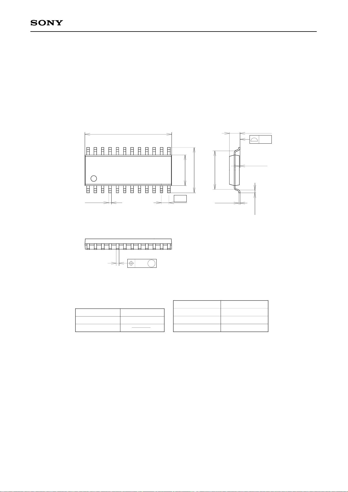
Package Outline Unit : mm
CXA2568M
—17—
 Loading...