

Page 1

– 1 –
CXA2525AM/AN
E96318C8Z
RF Amplifier for CD Player and CD-ROM
Description
The CXA2525AM/AN is an IC for RF signal
processing of CD player and CD-ROM.
Features
• Wide-band RF amplifier. (RF signal fc ≥ 12MHz)
• RF equalizer (T type)
• EFM time constant can be adjusted
(with switching function)
• APC (Automatic Power Control) function
• Power saving function
Functions
• RF summing amplifier
• RF equalizer
• Focus error amplifier
• Tracking error amplifier
• APC circuit
Absolute Maximum Ratings
• Supply voltage VCC 7V
•Storage temperature Tstg –65 to +150 °C
• Allowable power dissipation
PD 500 mW
Operating Conditions
• Supply voltage VCC – GND +3.0 to +5.5 V
• Operating temperature Topr –20 to +75 °C
Applications
• CD players
• CD-ROM drives
Sony reserves the right to change products and specifications without prior notice. This information does not convey any license by
any implication or otherwise under any patents or other right. Application circuits shown, if any, are typical examples illustrating the
operation of the devices. Sony cannot assume responsibility for any problems arising out of the use of these circuits.
CXA2525AM
20 pin SOP (Plastic)
CXA2525AN
20 pin SSOP (Plastic)
For the availability of this product, please contact the sales office.
Page 2
– 2 –
CXA2525AM/AN
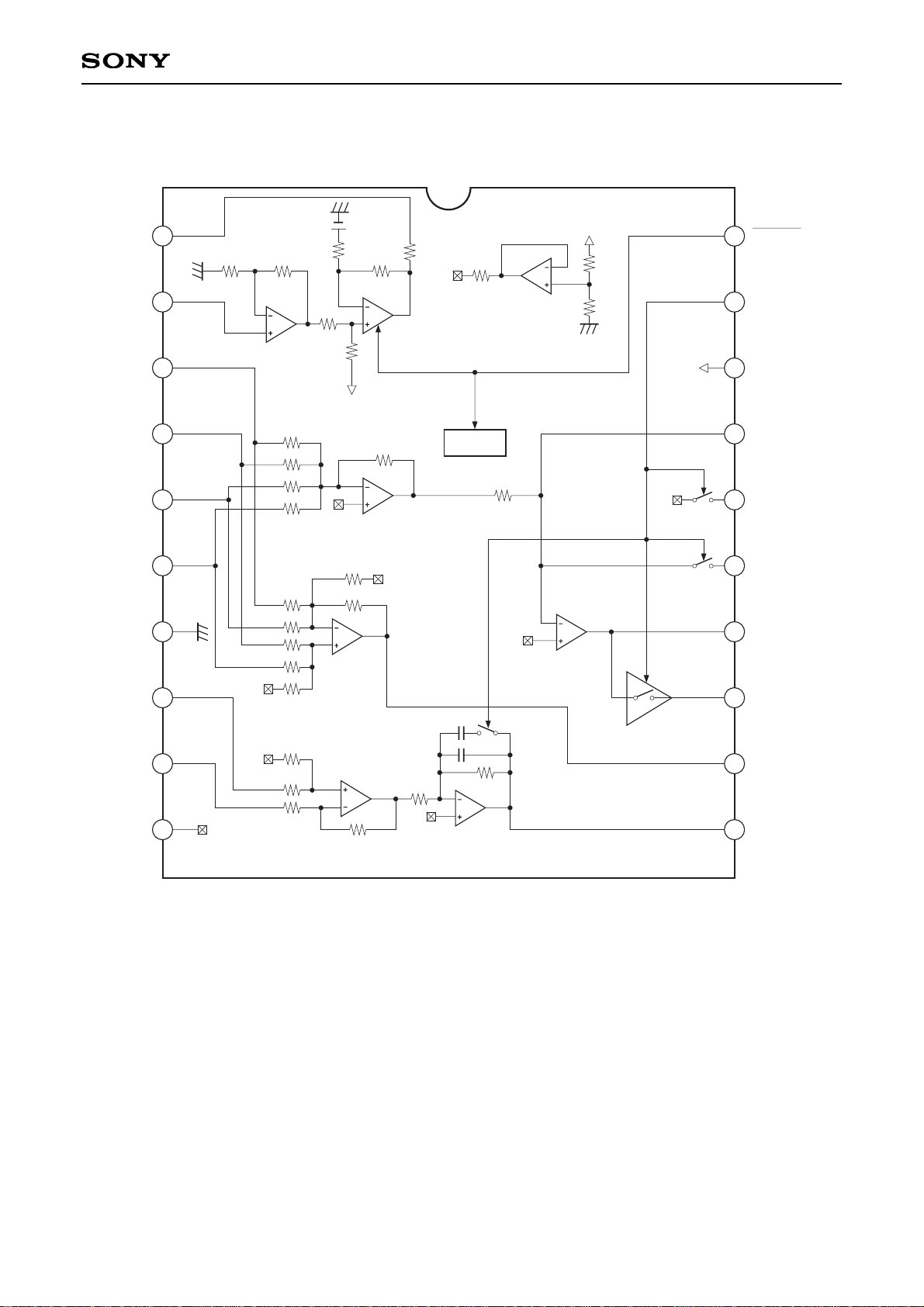
Block Diagram
LD
PD
A
B
C
D
GND
E
F
VC
APC_ON
MODE
VCC
RF_M
BPF_SW
LPF_SW
RFO_1
RFO_2
FE
TE
2
3
4
5
6
7
8
9
10
1
11
12
13
14
15
16
17
18
19
20
BGR
VC
BUFFER
40k
40k
V
CC
25
1k
10k
V
CC
56k
10k
55k 56k10k
1.25V
APC
Standby
10k
10k
10k
10k
10k
64k
64k
64k
64k
174k
348k
348k
2k
VC
V
CC
RF
Summing
Amp
Focus
Error Amp
RF Drive
Amp
VC
11p
5p
320k
VC
VC
112k
73.4k
112k
44k
44k
Tracking
Error Amp
Tracking
Drive Amp
Page 3
– 3 –
CXA2525AM/AN
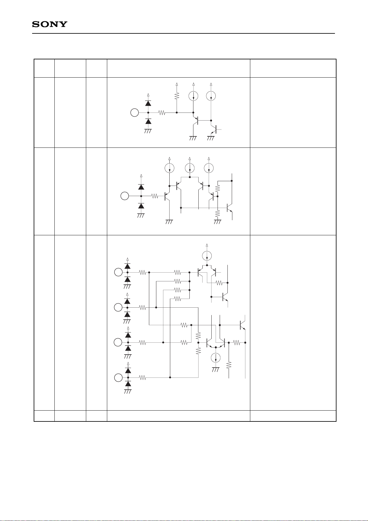
Pin Description
Pin
No.
Symbol I/O Equivalent circuit Description
1
LD
O
APC amplifier output.
1k
1
10k
2
PD
I
APC amplifier input.
7
GND
Ground.
8k
55k
10k
2
3
4
5
6
A
B
C
D
I
I
I
I
Input of RF summing
amplifier and focus error
amplifier.
10k
10k
10k
10k
10k
3
4
5
6
124
124
124
124
64k
64k
64k
64k
348k
348k
Page 4
– 4 –
CXA2525AM/AN
8
9
11
E
F
TE
I
I
O
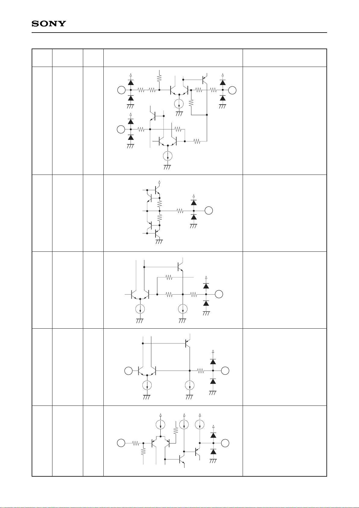
Tracking error amplifier input
for Pins 8 and 9;
tracking error drive output for
Pin 11.
8
9
11
124
44k
112k
124
44k
112k
320k
73.4k
124
10
VC
O
(VCC + GND) / 2 DC voltage
output.
120
120
25
10
12
FE
O
Focus error amplifier output
for Pin 12.
12
348k
348k
124
13
RFO_2
O
Buffer switch output which
sets the RF signal time
constant.
OFF when Pin 19 is
connected to VCC, ON when
it is connected to GND.
124
13
14
14
17
RFO_1
RF_M
O
I
Non-inversion input of RF
drive amplifier for Pin 17;
RF signal output for Pin 14;
resistance value connected
between Pins 14 and 17
which determines the low
frequency gain of RF drive
amplifier.
14
17
124
2k
1k
Pin
No.
Symbol I/O Equivalent circuit Description
Page 5
– 5 –
CXA2525AM/AN
15
LPF_SW
O
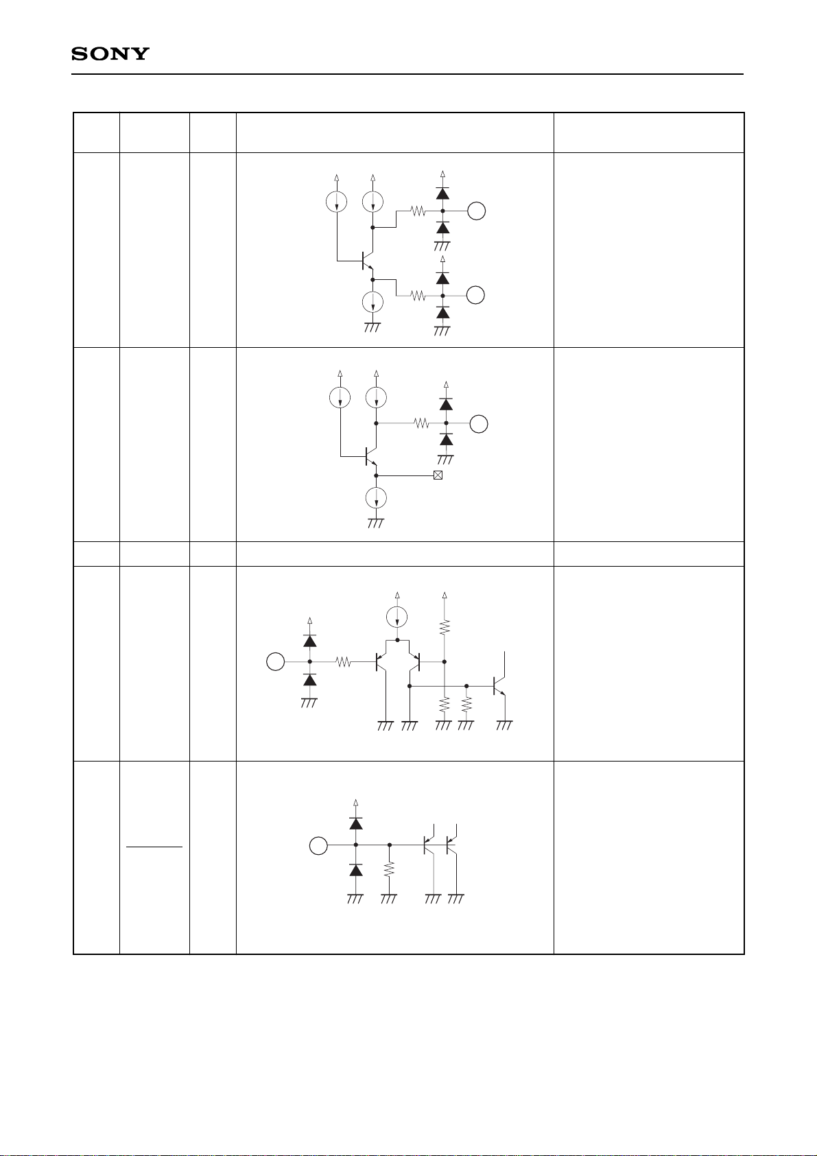
Transistor switch output
which sets the LPF cut-off
frequency of RF amplifier.
OFF when Pin 19 is
connected to VCC, ON when
it is connected to GND.
15
17
124
124
16
BPF_SW
O
Transistor switch output
which sets the RF amplifier
BPF boost.
OFF when Pin 19 is
connected to VCC, ON when
it is connected to GND.
124
VC
16
19
MODE
I
Multiple-speed mode
switching input.
VCC : High multiple-speed
mode
GND: Low multiple-speed
mode
124
19
50k
50k 30k
18
VCC
VCC.
20
APC_ON
I
APC amplifier ON/OFF
switching.
OFF when connecting to VCC;
ON when connecting to GND.
20
100k
Pin
No.
Symbol I/O Equivalent circuit Description
Page 6
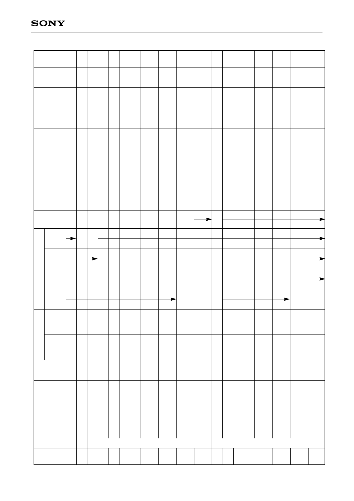
– 6 –
CXA2525AM/AN
Current consumption
Current consumption
Standby current
Offset voltage
Offset voltage
Voltage gain
Voltage gain
Voltage gain
Frequency
response
Frequency
response
Maximum output
amplitude H
Maximum output
amplitude L
Offset voltage
Voltage gain 1
Voltage gain 2
Voltage gain difference
Frequency
response 1
Frequency
response 2
Maximum output
amplitude H
Maximum output
amplitude L
0V
300mV
–
300mV
0V
300mV
300mV
Measure-
ment No.
1
2
3
4
5
6
7
8
9
10
11
12
13
14
15
16
17
18
19
20
I
CC
IEE
Istb
V1-1
V1-2
G1-1
G1-2
G1-3
F1-1
F1-2
V1-2
V1-3
V2-1
G2-1
G2-2
G2-3
F2-1
F2-2
V2-2
V2-3
O
O
O
O
O
O
O
O
O
O
O
O
O
O
O
O
O
O
O
O
300mV
300mV
300mV
0V
2.0V
–2.0V
2.0V
–2.0V
–2.0V
2.0V
–2.0V
2.0V
–2.0V
2.0V
–2.0V
18
7
18
14
13
14
14
13
14
13
14
12
—
–12—–50
–50
16.5
16.5
16.5
–3
–3
1.3
—
–50
17.7
17.7
–3
–4
–4
1.9
—
7.4
–7.4
1.8
–10
100
20
20
20.3
—
—
2.3
–1.3
0
20.7
20.7
0
—
—
2.4
–2.3
12
—
3
120
300
23
23
23.3
—
—
—
–0.3
50
23.7
23.7
3
—
—
—
–1.9
mA
mA
mA
mV
mV
dB
dB
dB
dB
dB
V
V
mV
dB
dB
dB
dB
dB
V
V
Pin DC current measurement
Pin DC current measurement
Pin DC current measurement
Pin DC current measurement
Pin DC current measurement
V1 = 100mVpp, f = 100kHz
V1 = 100mVpp, f = 100kHz
V1 = 100mVpp, f = 100kHz
V1 = 100mVpp, f = 12MHz
Difference for G1-1
V1 = 100mVpp, f = 4MHz
Difference for G1-2
DC voltage measurement
DC voltage measurement
DC voltage measurement
V1 = 100mVpp, f = 1kHz
V1 = 100mVpp, f = 1kHz
G2-1 to G2-2
V1 = 100mVpp, f = 20kHz
Difference for G2-1
V1 = 100mVpp, f = 20kHz
Difference for G2-2
DC voltage measurement
DC voltage measurement
Measurement item
Symbol
SW conditions
S1 S2 S3 S4 E1 E2 E3 E4
Bias conditions
Measure-
ment
point
Description of output waveform
and measurement method
Min. Typ. Max. Unit
RF amplifier
FE amplifier
Electrical Characteristics (Ta = 25°C, V
CC = 2.5V, GND = VC, VEE = –2.5V)
Page 7
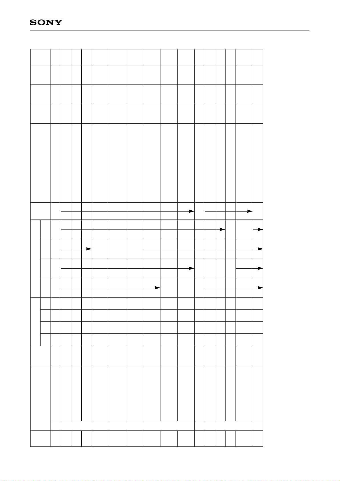
– 7 –
CXA2525AM/AN
Offset voltage
Voltage gain 1
Voltage gain 2
Voltage gain difference
Frequency
response 1
Frequency
response 2
Frequency
response 3
Frequency
response 4
Maximum output
amplitude H
Maximum output
amplitude L
Offset voltage 1
Offset voltage 2
Offset voltage 3
Offset voltage 4
Offset voltage 5
Offset voltage
11
1
10
–2.0V
2.0V
–2.0V
0V
69mV
123mV
177mV
0V
0V
300mV
300mV
0V
2.0V
–2.0V
–2.0V
2.0V
21
22
23
24
25
26
27
28
29
30
31
32
33
34
35
36
V3-1
G3-1
G3-2
G3-3
F3-1
F3-2
F3-3
F3-4
V3-2
V3-3
V4-1
V4-2
V4-3
V4-4
V4-5
V5-1
O
O
O
O
O
O
O
O
–50
17.9
17.9
–3
–4
–4
–3
–3
1.9
—
—
–1.2
0.8
1.8
—
–0.1
0
20.9
20.9
0
—
—
—
—
—
—
–1.6
0.1
2.1
2.45
—
—
50
23.9
23.9
3
—
—
—
—
—
–1.9
–0.1
1.6
—
—
0
0.1
mV
dB
dB
dB
dB
dB
dB
dB
V
V
V
V
V
V
V
V
DC voltage measurement
V1 = 100mVpp, f = 1kHz
V1 = 100mVpp, f = 1kHz
G3-1 to G3-2
V1 = 100mVpp, f = 20kHz
Difference for G3-1
V1 = 100mVpp, f = 20kHz
Difference for G3-2
V1 = 100mVpp, f = 200kHz
Difference for G3-1
V1 = 100mVpp, f = 200kHz
Difference for G3-2
DC voltage measurement
DC voltage measurement
DC voltage measurement
DC voltage measurement
DC voltage measurement
DC voltage measurement
I1 = 0.8mADC,
DC voltage measurement
DC voltage measurement
S1 S2 S3 S4 E1 E2 E3 E4
TE amplifierAPCVC
Measure-
ment No.
Measurement item
Symbol
SW conditions Bias conditions
Measure-
ment
point
Description of output waveform
and measurement method
Min. Typ. Max. Unit
Page 8
– 8 –
CXA2525AM/AN
LD
PD
A
B
C
D
GND
E
F
VC
MODE
VCC
RF_M
BPF_SW
LPF_SW
RFO_1
RFO_2
FE
TE
BGR
VC
BUFFER
40k
40k
V
CC
25
1k
10k
VCC
56k
10k
55k
56k
10k
APC
Standby
10k
10k
10k
10k
10k
64k
64k
64k
64k
174k
348k
348k
2k
V
CC
RF
Summing
Amp
Focus
Error Amp
RF Drive
Amp
11p
5p
320k
112k
73.4k
112k
44k
44k
Tracking
Error Amp
Tracking
Drive Amp
10k
10k
10k
10k
3.9k
1k
E3
E4
VCC
VEE
VEE
S1
S2
S3
S4
V1
E1
33µ
3µ
V
EE
VCC
2
3
4
5
6
7
8
9
10
1
11
12
13
14
15
16
17
18
19
20
I1
E2
APC_ON
150p
510
1p
1.25V
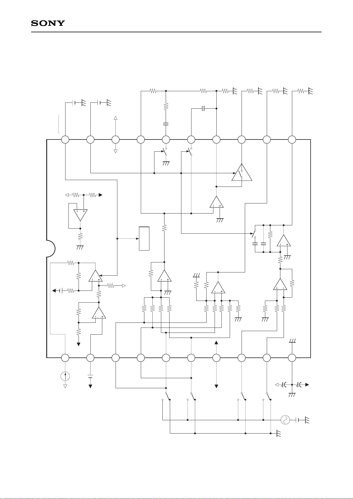
Electrical Characteristics Measurement Circuit
Page 9
– 9 –
CXA2525AM/AN
LD
PD
A
B
C
D
GND
E
F
VC
MODE
V
CC
RF_M
BPF_SW
LPF_SW
RFO_1
RFO_2
FE
TE
3.9k
1p
68p
390
1k
MODE
VCC
100µ
100
500
B IN
A IN
D IN
C IN
F IN
E IN
VC
22
10µ
1µ
1000p
Focus Error Out
Tracking Error Out
RF Out
4700p
BGR
VC
BUFFER
40k
40k
V
CC
25
1k
10k
V
CC
56k
10k
55k
56k
10k
APC
Standby
10k
10k
10k
10k
10k
64k
64k
64k
64k
174k
348k
348k
2k
VC
V
CC
RF
Summing
Amp
Focus
Error Amp
RF Drive
Amp
VC
11p
5p
320k
VC
VC
112k
73.4k
112k
44k
44k
Tracking
Error Amp
Tracking
Drive Amp
2
3
4
5
6
7
8
9
10
1
11
12
13
14
15
16
17
18
19
20
13p
APC_ON
VC
30k
1.25V
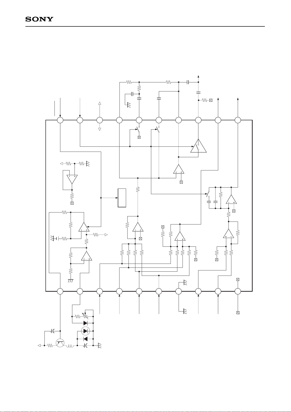
Application Circuit (Double-/sextuple-speed switching)
Application circuits shown are typical examples illustrating the operation of the devices. Sony cannot assume responsibility for
any problems arising out of the use of these circuits or for any infringement of third party patent and other right due to same.
Page 10
– 10 –
CXA2525AM/AN
Note on Operation
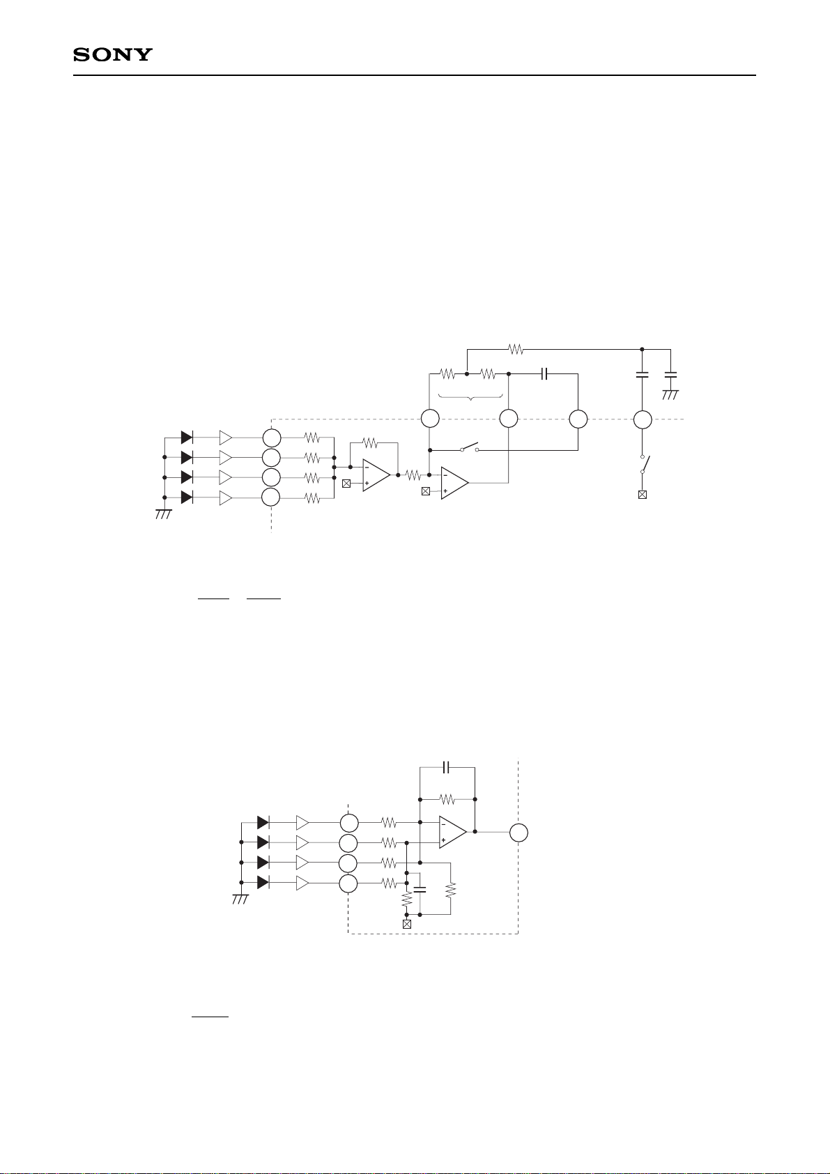
The RF AC maximum output amplitude is 1.3 Vpp when Pin 13 and 14 are capacitor-coupled shown in
Application Circuit.
Description of Operation
RF Amplifier
The signal currents from the photodiodes A, B, C and D are I-V converted, and input to Pins 3, 4, 5 and 6.
These signals are added at the RF summing amplifier and inverted at the RF drive amplifier and then output to
Pin 14.
The low frequency component of RFO output voltage is as follows:
VRFO = × × (A + B + C + D)
= 2.45 × (A + B + C + D)
Focus Error Amplifier
The operation of (B + D) – (A + C) is performed and the resulting signal is output to Pin 12.
The low frequency component of FE output voltage is as follows:
VFE = × (B + D – A – C)
= 5.43 × (B + D – A + C)
A
B
C
D
I-V
I-V
I-V
I-V
10k
10k
10k
10k
10k
2k
RFO
RF Drive Amp
VC
RF
Summing Amp
VC
RF_ M
3
4
5
6
17
14
1k163.9k
390
4.9k
1p
13p68p
15
LPF_SW
BPF_SW
10k
10k
4.9k
2k
A
B
C
D
I-V
I-V
I-V
I-V
64k
64k
64k
64k
348k
Focus
Error Amp
348k
15P
FE
15P
VC
174k
3
4
5
6
12
348k
64k
Page 11
– 11 –
CXA2525AM/AN
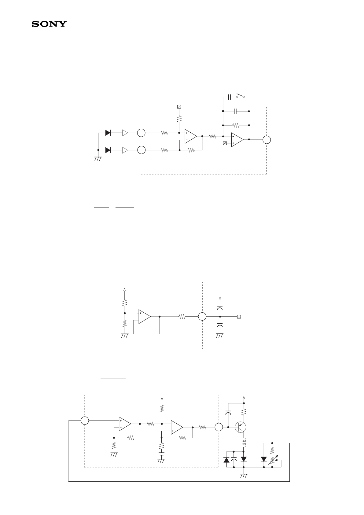
Tracking Error Amplifier
Each signal current from the photodiodes E and F is I-V converted and input to Pins 8 and 9. These signals
undergo operational amplification at the tracking error amplifier and tracking drive amplifier, and are output to
Pin 12.
The low frequency component of TE output voltage is as follows:
VTE = × × (F – E)
= 11.1 × (F – E)
Center Voltage Generation Circuit
The center voltage of VR = (VCC + GND) is supplied.
The maximum current is approximately ±3mA.
APC Circuit
When the laser diode is driven with constant current, the optical output possesses large negative temperature
characteristics. Therefore, the current must be controlled with the monitor photodiode to ensure the output
remains constant. When APC_ON pin is connected to GND, APC is ON; connected to VCC, it is OFF.
E
F
I-V
44k
320k
5P
TE
73.4k
VC
VC
112k
I-V
44k 112k
8
9
12
11P
112k
44k
320k
73.4k
VR
25
VC
40k
40k
Vc Buffer
Vcc
Vcc
10
PD
10k
55k 56k
10k
22
100
500
100µ
10µH
1µ
LD
1k
56k
V
CC
10k
1
2
1.25V
Page 12

– 12 –
CXA2525AM/AN
Example of Representative Characteristics
MODE = LOW
MODE = HIGH
MODE = LOW
MODE = HIGH
30
20
10
0
100k 1M 10M 100M
FREQ. [Hz]
GAIN [dB]
RFO_1 Frequency Response (W/O EQ)
30
20
10
0
100k 1M 10M 100M
FREQ. [Hz]
GAIN [dB]
RFO_2 Frequency Response (W/O EQ)
30
20
10
0
1k 10k 100k 1M
FREQ. [Hz]
GAIN [dB]
TE_Out Frequency Response
30
20
10
0
100k 1M 10M 100M
FREQ. [Hz]
GAIN [dB]
RF_Out Frequency Response (T-EQ)
∗
30
20
10
0
100 1k 10k 100k
FREQ. [Hz]
GAIN [dB]
FE_Out Frequency Response
2.5
2.0
1.5
1.0
0 100 200 300
PD [mV]
LD [V]
APC Characteristics
0.5
0
–0.5
–1.0
–1.5
–2.0
∗
T-EQ As shown in Application Circuit
Page 13
– 13 –
CXA2525AM/AN
SONY CODE
EIAJ CODE
JEDEC CODE
SOP-20P-L01
∗SOP020-P-0300-A
PACKAGE STRUCTURE
PACKAGE MATERIAL
LEAD TREATMENT
LEAD MATERIAL
PACKAGE WEIGHT
COPPER ALLOY
SOLDER PLATING
EPOXY / PHENOL RESIN
0.3g
20PIN SOP (PLASTIC) 300mil
12.45 – 0.1
+ 0.4
20
11
0.45 ± 0.1
1.27
10
1
5.3 – 0.1
+ 0.3
7.9 ± 0.4
6.9
0.2 – 0.05
+ 0.1
0.5 ± 0.2
0.1 – 0.05
+ 0.2
1.85 – 0.15
+ 0.4
0.15
± 0.12
M
CXA2525AN
20PIN SSOP (PLASTIC)
SONY CODE
EIAJ CODE
JEDEC CODE
PACKAGE STRUCTURE
PACKAGE MATERIAL
LEAD TREATMENT
LEAD MATERIAL
PACKAGE WEIGHT
EPOXY RESIN
SOLDER / PALLADIUM
COPPER / 42 ALLOY
0.1g
SSOP-20P-L01
SSOP020-P-0044
0.1 ± 0.1
0.5 ± 0.2
0° to 10°
DETAIL A
PLATING
∗6.5 ± 0.1
∗4.4 ± 0.1
0.22 – 0.05
+ 0.1
0.65 ± 0.12
20
11
10
1
A
0.1
+ 0.05
1.25 – 0.1
+ 0.2
0.15 – 0.02
6.4 ± 0.2
NOTE: Dimension “∗” does not include mold protrusion.
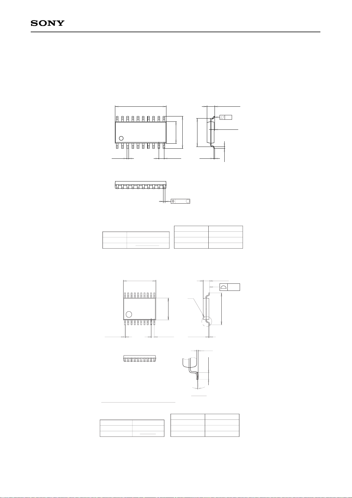
Package Outline Unit: mm
CXA2525AM
NOTE : PALLADIUM PLATING
This product uses S-PdPPF (Sony Spec.-Palladium Pre-Plated Lead Frame).
 Loading...