

Page 1
Description
The CXA2089Q/S is a 5-input, 2-output audio/video
switch featuring I2C bus compatibility for TVs. This IC
has input pins that are compatible with S2 protocol.
Features
• 3 inputs that are compatible with S2 protocol
• Serial control with I2C bus
• 5 inputs, 2 outputs
• The desired inputs can be selected independently
for each of the 2 outputs
• Wide band video amplifier (20MHz, –3dB)
• Y/C MIX circuit
• Slave address can be changed (90H/92H)
• Audio muting from external pin
• High impedance maintained by I2C bus lines (SDA,
SCL) even when power is OFF
• Wide audio dynamic range (3Vrms typ.)
Applications
Audio/video switch featuring I2C bus compatibility
for TVs
Structure
Bipolar silicon monolithic IC
Absolute Maximum Ratings
• Supply voltage VCC 12 V
• Operating temperature Topr –20 to +75 °C
• Storage temperature Tstg –65 to +150 °C
• Allowable power dissipation
PD 1500 mW
Operating Conditions
Supply voltage 9 ± 0.5 V
– 1 –
CXA2089Q/S
E97431B7Z-PS
S2-Compatible 5-Input 2-Output Audio/Video Switch
Sony reserves the right to change products and specifications without prior notice. This information does not convey any license by
any implication or otherwise under any patents or other right. Application circuits shown, if any, are typical examples illustrating the
operation of the devices. Sony cannot assume responsibility for any problems arising out of the use of these circuits.
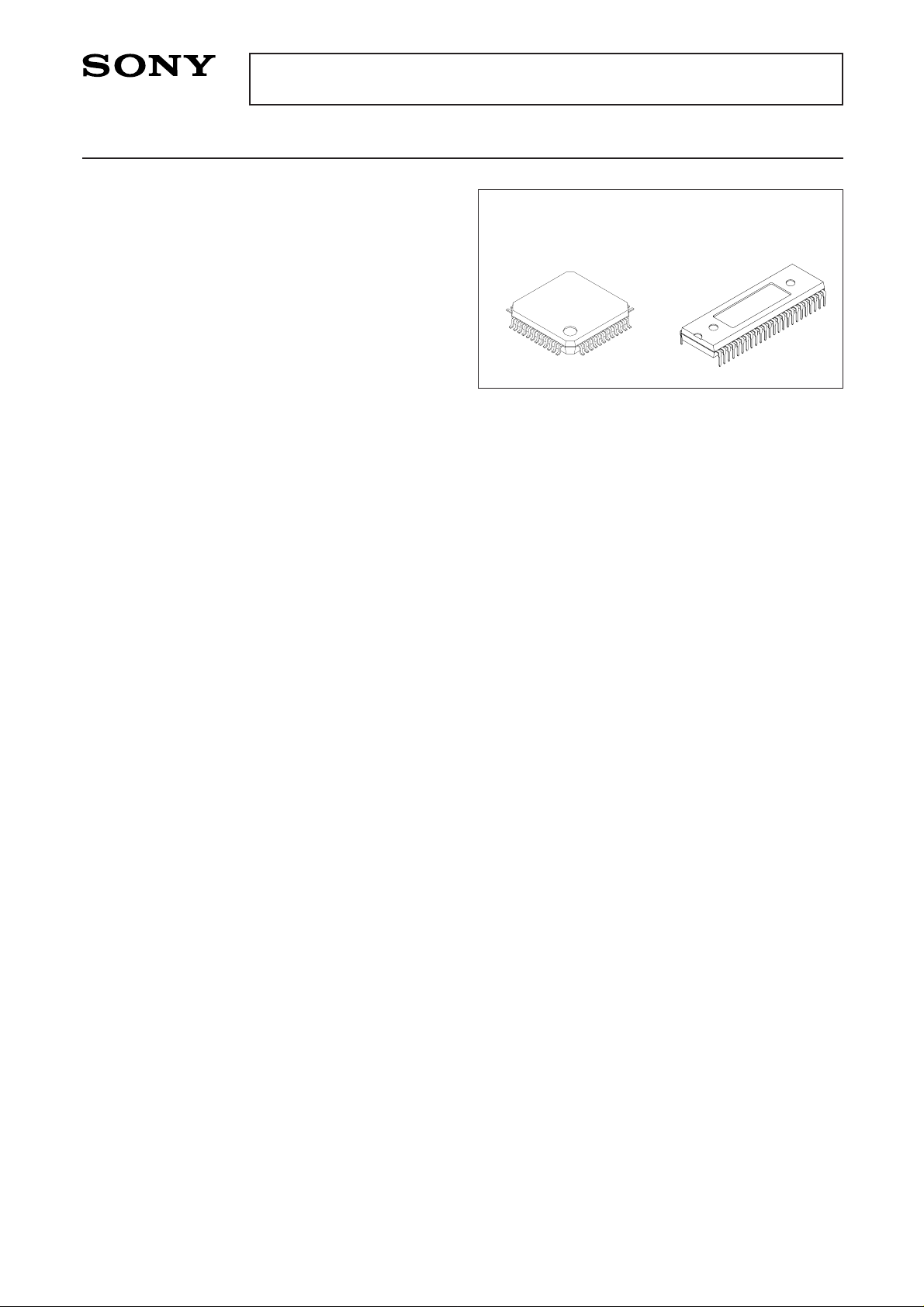
CXA2089Q
48 pin QFP (Plastic)
CXA2089S
48 pin SDIP (Plastic)
Page 2
– 2 –
CXA2089Q/S
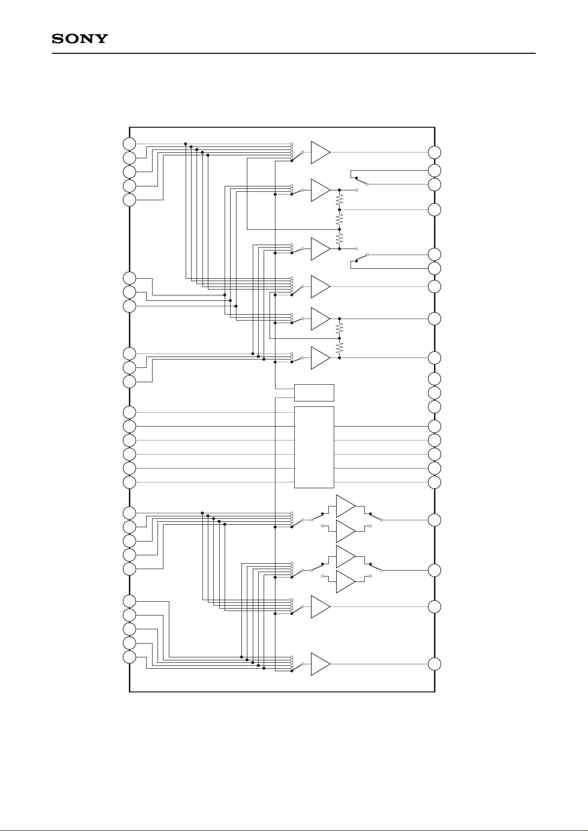
Block Diagram
CXA2089Q
47
VOUT1
YOUT1
TV
V4
V3
V2
V1
Y3
Y2
Y1
C3
C2
C1
YIN1
TRAP1
GND
COUT1
CIN1
VOUT2
YOUT2
COUT2
BIAS
V
CC
6dB
6dB
6dB
6dB
6dB
6dB
BIAS
40
38
37
42
43
44
45
ADR
SDA
SCL
DC OUT
MUTE
Logic
27
28
36
34
33
8
15
1
3
5
10
12
17
19
26
23
32
S-3
S2-1
LTV
LV4
S-2
S-1
S2-3
S2-2
LV3
LV2
LV1
LOUT1
ROUT1
LOUT2
ROUT2
6dB
0dB
6dB
0dB
6dB
6dB
39
41
30
22
2
9
16
6
7
13
14
20
21
46
RTV
RV4
RV3
RV2
RV1
31
29
48
4
11
18
24
35
25
Audio system is attenuated by 6dB for 6kΩ resistor input, and a total gain is 0dB (LOUT1 and ROUT1 can be changed to –6dB).
Page 3
– 3 –
CXA2089Q/S
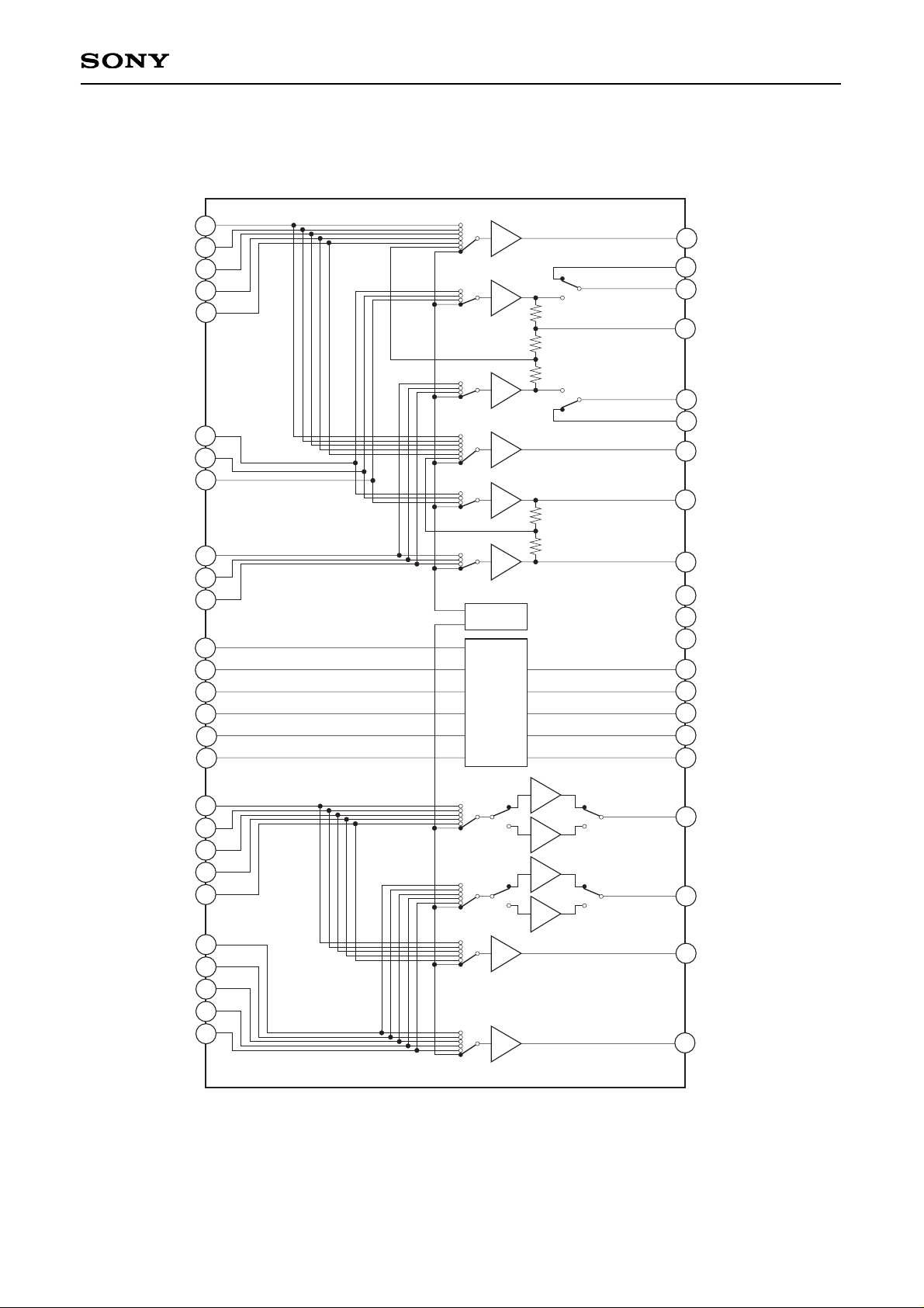
CXA2089S
VOUT1
YOUT1
TV
V4
V3
V2
V1
Y3
Y2
Y1
C3
C2
C1
YIN1
TRAP1
GND
COUT1
CIN1
VOUT2
YOUT2
COUT2
BIAS
V
CC
6dB
6dB
6dB
6dB
6dB
6dB
BIAS
ADR
SDA
SCL
DC OUT
MUTE
Logic
S-3
S2-1
LTV
LV4
S-2
S-1
S2-3
S2-2
LV3
LV2
LV1
LOUT1
ROUT1
LOUT2
ROUT2
6dB
0dB
6dB
0dB
6dB
6dB
RTV
RV4
RV3
RV2
RV1
5
7
14
21
29
9
16
23
11
18
25
12
19
26
13
20
27
4
8
15
22
28
6
10
17
24
30
46
42
1
48
3
44
39
37
35
2
43
34
32
33
31
41
40
45
47
36
38
Audio system is attenuated by 6dB for 6kΩ resistor input, and a total gain is 0dB (LOUT1 and ROUT1 can be changed to –6dB).
Page 4
13
14
15
16
17
18
19
20
21
22
23
24
25
26
27
28
29
30
36
35
34
31
32
33
40
39
38
37
41
42
43
44
45
46
47
48
2
3
4
5
6
7
8
9
10
11
121
BIAS
CIN1
LOUT1
VOUT1
ROUT1
TRAP1
YOUT1
GND
COUT1
LTV
TV
RTV
RV4
V4
LV4
S-3
S2-3
C3
RV3
Y3
LV3
V3
S-2
S2-2
YIN1
MUTE
V
CC
VOUT2
ROUT2
YOUT2
LOUT2
COUT2
DC OUT
SDA
SCL
ADR
V1
LV1
Y1
RV1
C1
S2-1
S-1
V2
LV2
Y2
RV2
C2
– 4 –
CXA2089Q/S
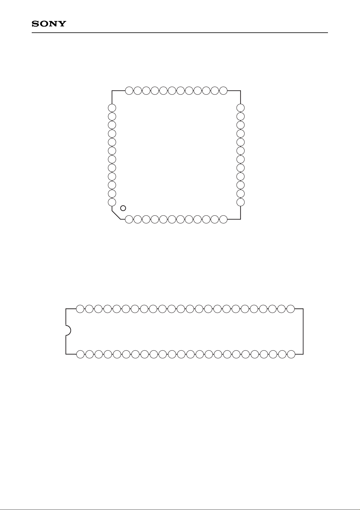
Pin Configuration
CXA2089Q
13
14 15
16
17
18
19
20
21
22
23
24
25
26
27
28
29
30
36
35
34
31
32
33
40
39
38
37
41
42
43
44
45
46
47
48
2
3
4
5
6
7
8
9
10
11
121
BIAS
CIN1
LOUT1
VOUT1
ROUT1
TRAP1
YOUT1
GND
COUT1
LTV
TV
RTV
RV4
V4
LV4
S-3
S2-3
C3
RV3
Y3
LV3
V3
S-2
S2-2
YIN1
MUTE
V
CC
VOUT2
ROUT2
YOUT2
LOUT2
COUT2
DC OUT
SDA
SCL
ADR
V1
LV1
Y1
RV1
C1
S2-1
S-1
V2
LV2
Y2
RV2
C2
CXA2089S
Page 5
– 5 –
CXA2089Q/S
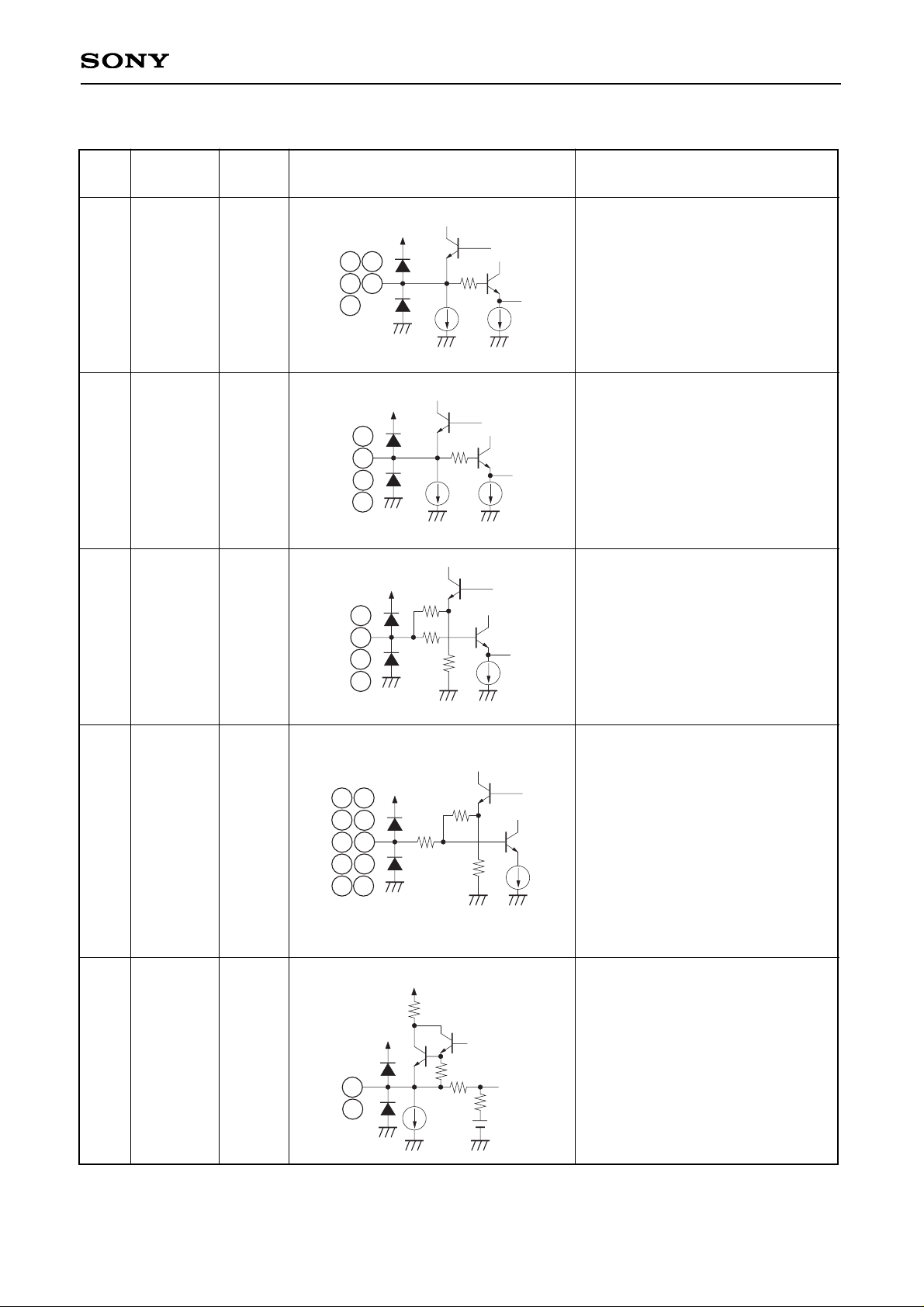
Pin Description Pin numbers in brackets are for the CXA2089S.
Pin
No.
47 (5)
1 (7)
8 (14)
15 (21)
23 (29)
TV
V1
V2
V3
V4
4.0V
Video signal inputs.
Input composite video signals.
Symbol
Pin
voltage
Equivalent circuit Description
150
VCC
3µA
47
1
15
23
8
3 (9)
10 (16)
17 (23)
36 (42)
Y1
Y2
Y3
YIN1
4.0V
Y/C separation signal inputs.
Input luminance signals.
The YIN1 pin inputs the signal
obtained by Y/C separating the
VOUT1 pin output.
3
10
17
150
VCC
3µA
36
5 (11)
12 (18)
19 (25)
38 (44)
C1
C2
C3
CIN1
4.5V
Y/C separation signal inputs.
Input chrominance signals.
The CIN1 pin inputs the signal
obtained by Y/C separating the
VOUT1 pin output.
150
V
CC
27k
20k
5
12
19
38
46 (4)
2 (8)
9 (15)
16 (22)
22 (28)
48 (6)
4 (10)
11 (17)
18 (24)
24 (30)
LTV
LV1
LV2
LV3
LV4
RTV
RV1
RV2
RV3
RV4
4.5V Audio signal inputs.
VCC
15k
33k
27k
2
4
9
11
16
18
46
48
22
24
40 (46)
33 (39)
VOUT1
VOUT2
3.9V
Video signal outputs.
Output composite video signals.
VCC
27k
VCC
23.5k
30k
250
40
33
Page 6
– 6 –
CXA2089Q/S
45 (3)
29 (35)
COUT1
COUT2
4.5V
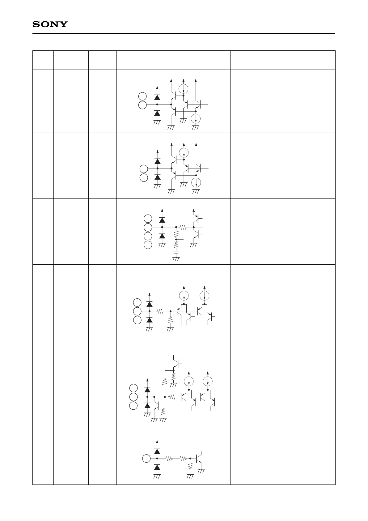
Video signal outputs.
Output chrominance signals.
VCC
VCC VCC VCC
45
29
43 (1)
YOUT1
3.3V
31 (37)
YOUT2
3.5V
Video signal outputs.
Output luminance signals.
VCC
VCC VCC VCC
43
31
39 (45)
30 (36)
41 (47)
32 (38)
LOUT1
LOUT2
ROUT1
ROUT2
4.5V
Audio signal outputs.
Zo = 50Ω (within DC ± 2mA)
VCC
VCCVCC
147
100k
6
13
20
6 (12)
13 (19)
20 (26)
S2-1
S2-2
S2-3
—
Detects the S2-compatible DC
superimposed onto the C signal.
4:3 video signal at 1.3V or less
4:3 letter-box signal at 1.3V or more
to 2.5V or less
16:9 picture squeezed signal at 2.5V
or more
These pins are pulled down to GND
by a 100kΩ resistor, so the 4:3 video
signals are selected when open.
VCC VCC
20k
56
20k
39
30
41
32
7 (13)
14 (20)
21 (27)
S-1
S-2
S-3
—
Composite video/S selector.
The detection results are written to
the status register.
S signal at 3.5V or less
Composite video signal at 3.5V or
more
These pins are pulled up to 5V by a
100kΩ resistor, so the composite
video signals are selected when
open.
VCC
VCCVCC
50k
10k
100k
50k
5V
7
14
21
25 (31)
ADR —
Selects the slave address for the I2C
bus.
90H at 1.5V or less
92H at 2.5V or more
90H when open
VCC
147
28k
72k
25
Pin
No.
Symbol
Pin
voltage
Equivalent circuit Description
Page 7

– 7 –
CXA2089Q/S
27 (33)
SDA
—
I2C bus signal input
VILmax = 1.5V
VIHmin = 3.0V
VOLmax = 0.4V
VCC
4k
27
26 (32)
SCL
—
I2C bus signal input
VILmax = 1.5V
VIHmin = 3.0V
VCC
4k
10k
26
28 (34)
DC OUT —
Outputs the S2-compatible DC
superimposed onto the COUT2
output. The DC is superimposed by
connecting this pin to the COUT2
output via a capacitor.
Control is performed by the I2C bus.
When 0V is output, Q1 is ON and
the impedance is 5kΩ.
S2 protocol output DC impedance of
10 ± 3kΩ is realized by attaching
external resistance of 4.7kΩ.
DC OUT (bus) Output DC
0 4.5V
1 0V
2 1.9V
3 4.5V
VCC
100
1k
42
42 (48)
TRAP1 3.8V
Connects trap circuit for subcarrier.
VCC
4k
28k
1k
Q1
28
35 (41)
MUTE —
Audio signal output mute.
Mute OFF at 1.5V or less
Mute ON at 2.5V or more
Mute OFF when open
VCC
147
28k
72k
35
37 (43)
BIAS 4.5V
Internal reference bias (Vcc/2).
Connects to GND via a capacitor.
VCC
VCC
147
20k
VCC
20k
37
Pin
No.
Symbol
Pin
voltage
Equivalent circuit Description
Page 8
– 8 –
CXA2089Q/S
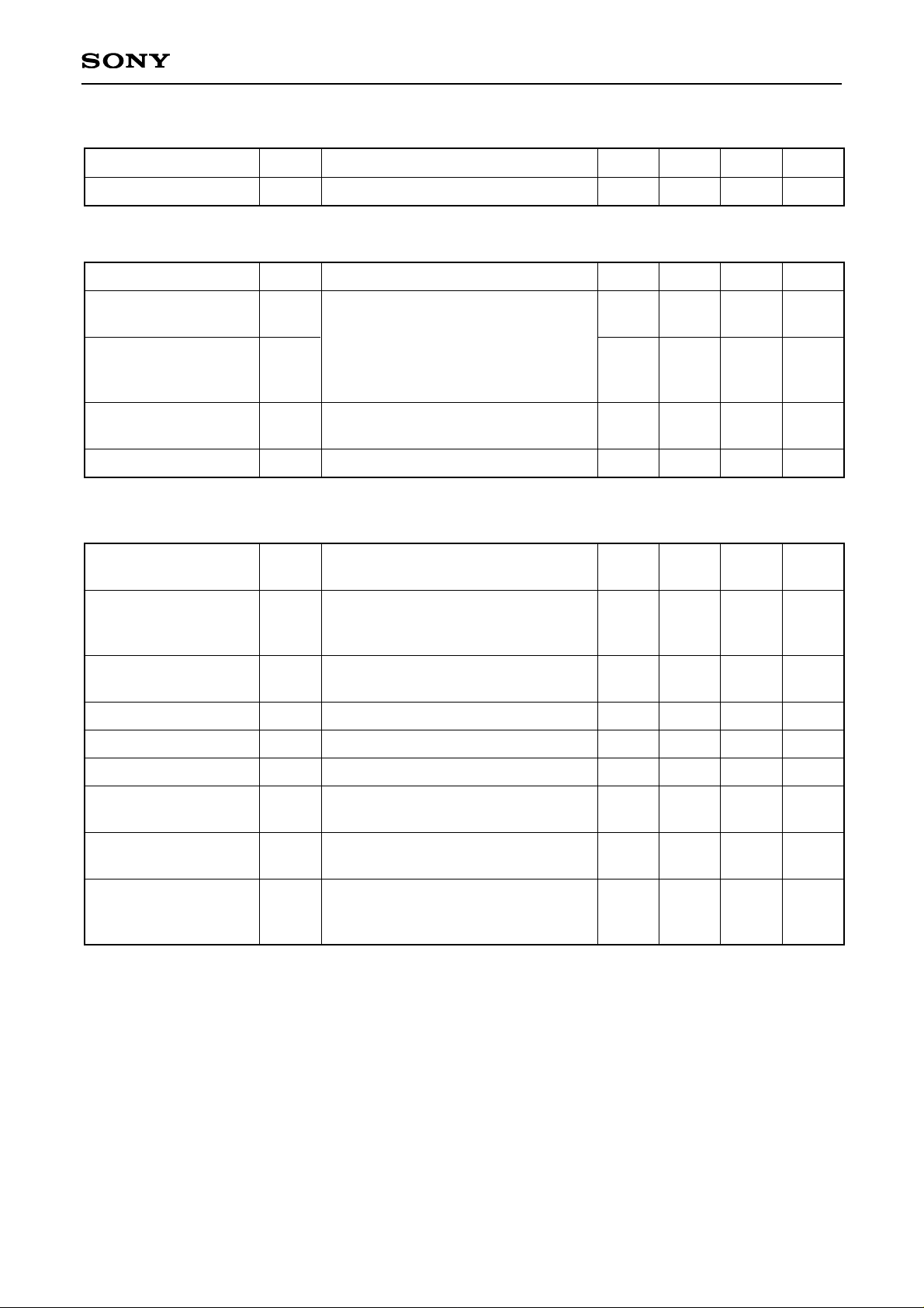
Electrical Characteristics (Ta = 25°C, VCC = 9V)
Item
Current consumption ICC No signal, no load 30 45 62 mA
Symbol Conditions Min. Typ. Max. Unit
Video system (Measurement circuit; Fig. 1)
Gain
Frequency response
characteristics
Frequency response
characteristics
(Y/C mix)
Input dynamic range
Cross talk
GVv
FBWv1
FBWv2
Ddv
Vctv
f = 100kHz, 0.3Vp-p input
f = 100kHz, input frequency where
output amplitude is –3dB with 0.3Vp-p
output serving as 0dB
f = 100kHz,
maximum with distortion < 1.0%
f = 4.43MHz, 1Vp-p input
5.9
15
10
1.4
—
6.4
20
15
—
—
6.9
—
—
—
–50
dB
MHz
MHz
Vp-p
dB
Audio system (Measurement circuits; Fig. 2 to Fig. 5)
Gain
Frequency response
characteristics
Total harmonic
distortion
Input dynamic range
Cross talk
Ripple rejection ratio
Output DC offset
Residual noise
S/N ratio
GVA
FBWA
THD
DdA
VctA
VctA
Voff
VNA
S/N
f = 1kHz, 1Vp-p input,
5.7kΩ resistor inserted to input
f = 1kHz, input frequency where
output amplitude is –3dB with 1Vp-p
output serving as 0dB
f=1kHz, 2.2Vp-p input, where 400Hz
HPF + 80kHz LPF are inserted
f=1kHz, maximum with distortion < 0.3%
f=1kHz, 1Vp-p input
f=100Hz, 0.3Vp-p applied to Vcc
Offset voltage between input and
output
When 400Hz HPF+ 30kHz LPF are
inserted
f=1kHz, 1Vrms input
When 400Hz HPF + 30kHz LPF are
inserted
–1
50
—
2.8
—
—
–30
0
0
—
0.03
3.0
–90
–55
—
20
–100
1
—
0.05
—
–80
–40
30
30
–90
dB
kHz
%
Vrms
dB
dB
mV
µVrms
dB
Page 9
– 9 –
CXA2089Q/S
High level input voltage
Low level input voltage
Low level output voltage
High level input current
Low level input current
Maximum clock
frequency
Minimum waiting time
for data change
Minimum waiting time
for data transfer start
Low level clock pulse
width
High level clock pulse
width
Minimum waiting time
for start preparation
Minimum data hold time
Minimum data
preparation time
Rise time
Fall time
Minimum waiting time
for stop preparation
VIH
VIL
VOL
IIH
IIL
fSCL
tBUF
tHD;STA
tLOW
tHIGH
tSU;STA
tHD;DAT
tSU;DAT
tR
tF
tSU;STO
With SDA 3mA current supplied
VIH = 4.5V
VIL = 0.4V
3.0
0
0
0
0
0
4.7
4.0
4.7
4.0
4.7
150
0
—
—
4.7
—
—
—
—
—
—
—
—
—
—
—
—
—
—
—
—
5.0
1.5
0.4
10
10
100
—
—
—
—
—
—
—
1
300
—
V
V
V
µA
µA
kHz
µs
µs
µs
µs
µs
ns
ns
µs
ns
µs
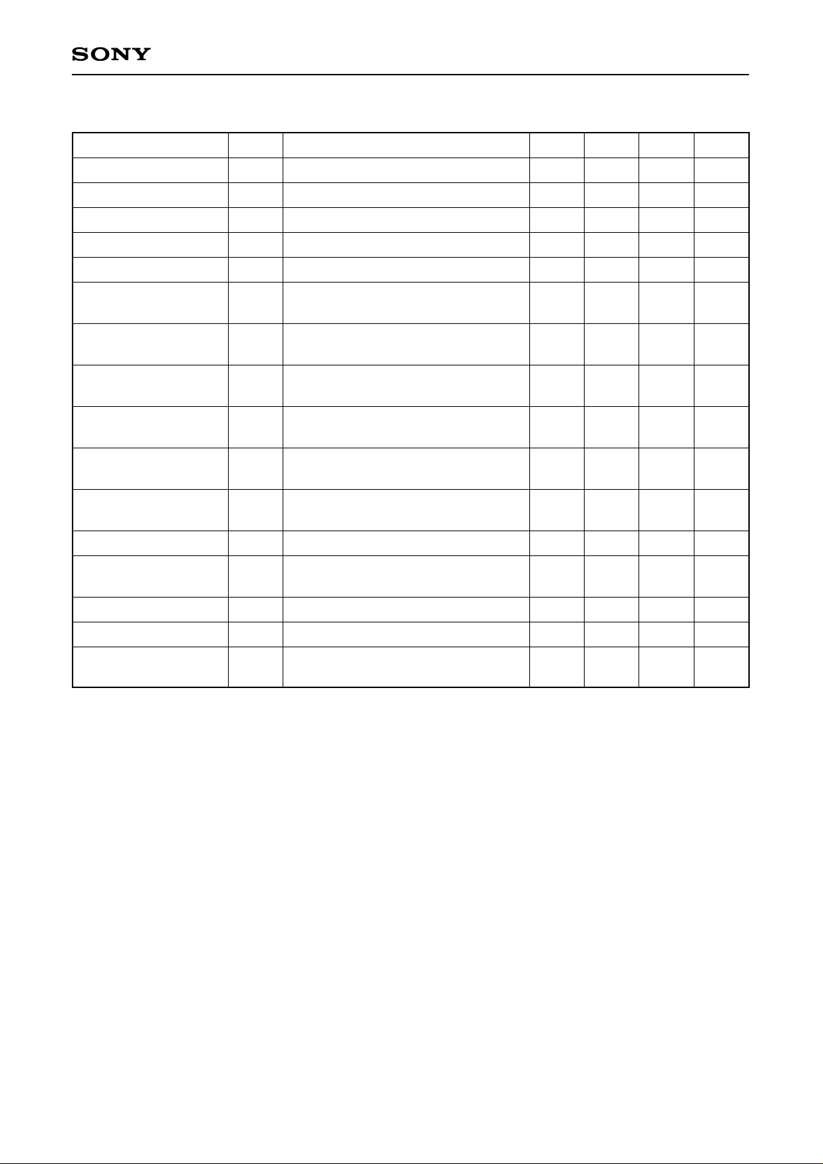
Logic system
Item Symbol Conditions Min. Typ. Max. Unit
Page 10
– 10 –
CXA2089Q/S
0.1µ
75
10µ
10k
1µ
0.47µ
600
75
600
10µ
10k
10µ
10µ
10k
0.1µ0.47µ
75
1µ
0.47µ
1µ
75
75
0.1µ0.47µ
75
1µ
0.47µ
1µ
75
0.47µ
1µ
0.47µ
1µ
0.1µ
10µ
1µ
0.47µ
1µ
75
600
75
600
75
600 600
75
600 600
75
10µ
600
600
10k
10k
Input signal
0.47µ
75
22µ
1k
Measurement point
µ-com
10µ
10k
10µ
10k
10µ
10k
10µ
10k
10µ
10k
2
3
4
5
6
7
8
9
10
11
12
14
15
16
17
18
19
20
21
22
23
24
25
262728
29
30
35
34
31
32
33
40
39
38
37
41
42
43
44
45
46
47
48
1
BIAS
CIN1
LOUT1
VOUT1
ROUT1
TRAP1
YOUT1
GND
COUT1
LTV
TV
RTV
RV4
V4
LV4
S-3
S2-3
C3
RV3
Y3
LV3
V3
S-2
S2-2
YIN1
MUTE
V
CC
VOUT2
ROUT2
YOUT2
LOUT2
COUT2
DC OUT
SDA
SCL
ADR
V1
LV1
Y1
RV1
C1
S2-1
S-1
V2
LV2
Y2
RV2
C2
13
36
1µ
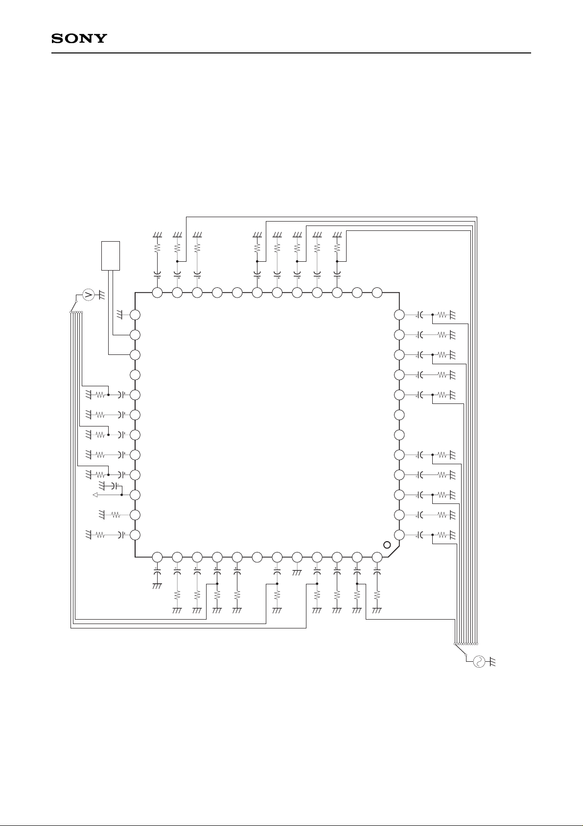
Fig. 1-a. Video system (gain, frequency response characteristics, input dynamic range, cross talk) measurement circuit (CXA2089Q)
Signal is input from one of the following pins: 1, 3, 5, 8, 10, 12, 15, 17, 19, 23 and 47.
Output signal is measured from one of the following pins: 29, 31, 33, 40, 43 and 45.
Electrical Characteristics Measurement Circuit
Page 11
– 11 –
CXA2089Q/S
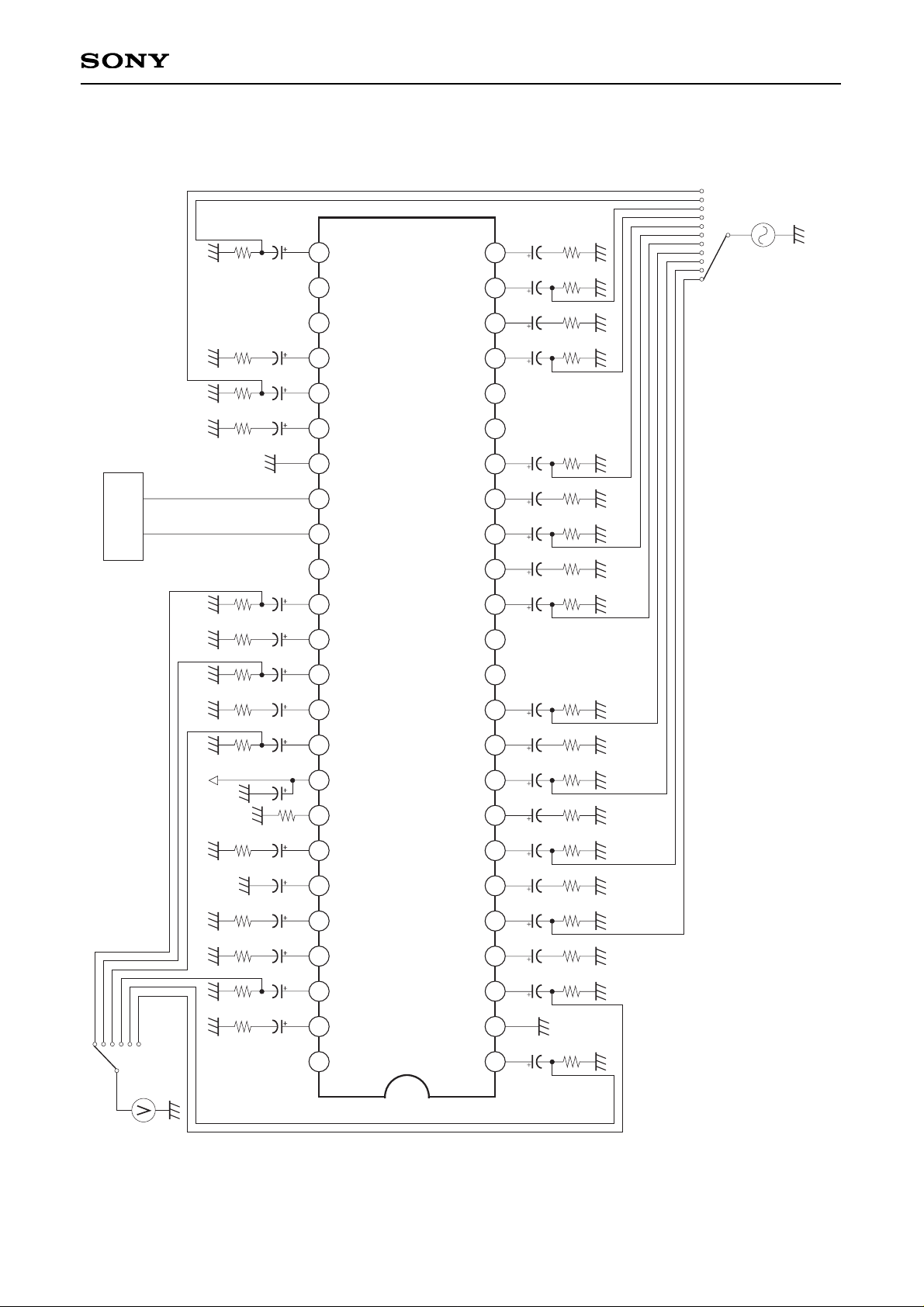
Signal is input from one of the following pins: 5, 7, 9, 11, 14, 16, 18, 21, 23, 25 and 29.
Output signal is measured from one of the following pins: 1, 3, 35, 37, 39 and 46.
RV4
V4
LV4
S-3
S2-3
C3
BIAS
CIN1
LOUT1
VOUT1
ROUT1
TRAP
YIN1
MUTE
V
CC
VOUT2
ROUT2
YOUT2
LOUT2
COUT2
DC-OUT
SDA
SCL
ADR
YOUT1
GND
COUT1
LTV
TV
RTV
RV3
Y3
LV3
V3
S-2
S2-2
V1
LV1
Y1
RV1
C1
S2-1
S-1
V2
LV2
Y2
RV2
C2
10µ 10µ 1µ 0.47µ 1µ 0.47µ 1µ 0.47µ 1µ 0.1µ 0.47µ 1µ 0.47µ 1µ 0.1µ 0.47µ 1µ 0.47µ 1µ
10k
10k
600
75
600
75
600
75
600
75 75
600
75
600
75
600
75
600
10k
10µ
10k
10µ
10k
0.1µ
75
10µ 0.47µ
75
1k
22µ
10µ
10k
10µ
10k
10µ
10k
10µ
10k
10µ
10k
1µ
600
0.47µ
75
1µ
600
0.1µ
75
10µ
+9V
75
µ-COM
1
4
5
6
7
8
9
10
2
3
11
12
13
14
15
16
17
18
19
20
21
22
23
24
25
26
27
28
29
30
31
32
33
34
35
36
37
38
39
40
41
42
43
44
45
46
47
48
Input signal
Measurement point
Fig. 1-b. Video system (gain, frequency response characteristics, input dynamic range, cross talk) measurement circuit (CXA2089S)
Page 12
– 12 –
CXA2089Q/S
0.1µ
75
10µ
10k
1µ
0.47µ
600
75
600
10µ
10k
10µ
10µ
10k
0.1µ
0.47µ
75
1µ
0.47µ
1µ
75 75
0.1µ
0.47µ
75
1µ
0.47µ
1µ
75
0.47µ
1µ
0.47µ
1µ
0.1µ
10µ
1µ
0.47µ
1µ
75
600
75
600
75
600 600
75
600 600
75
10µ
600
600
10k
10k
0.47µ
75
22µ
1k
µ-com
10µ
10k
10µ
10k
10µ
10k
10µ
10k
10µ
10k
2
3
4
5
6
7
8
9
10
11
12
14
15
16
17
18
19
20
21
22
23
24
25
26
2728
29
30
35
34
31
32
33
40
39
38
37
41
42
43
44
45
46
47
48
1
BIAS
CIN1
LOUT1
VOUT1
ROUT1
TRAP1
YOUT1
GND
COUT1
LTV
TV
RTV
RV4
V4
LV4
S-3
S2-3
C3
RV3
Y3
LV3
V3
S-2
S2-2
YIN1
MUTE
V
CC
VOUT2
ROUT2
YOUT2
LOUT2
COUT2
DC OUT
SDA
SCL
ADR
V1
LV1
Y1
RV1
C1
S2-1
S-1
V2
LV2
Y2
RV2
C2
13
36
1µ
5.7k
5.7k
5.7k
5.7k
5.7k
5.7k
5.7k5.7k
5.7k
5.7k
Input signal
Measurement point
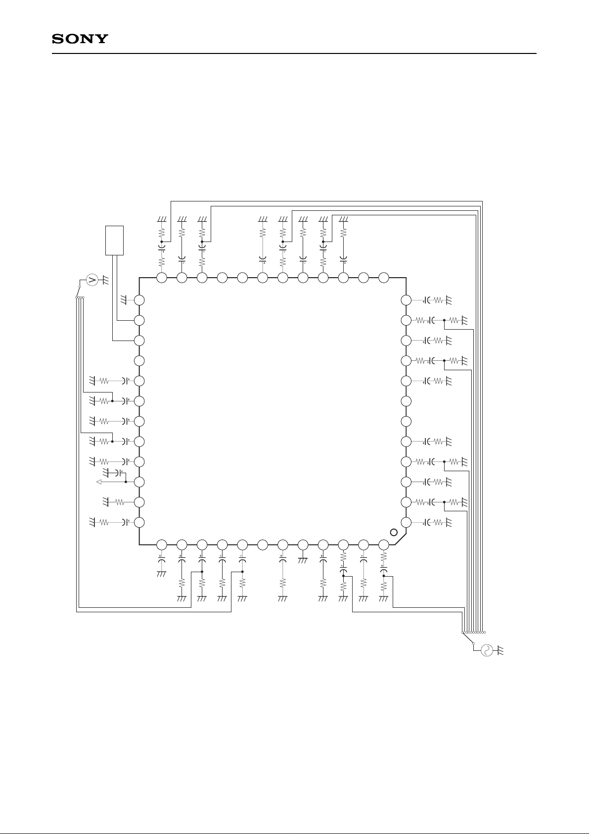
Fig. 2-a. Audio system (gain, frequency response characteristics, total harmonic distortion, input dynamic range, cross talk) measurement circuit (CXA2089Q)
Signal is input from one of the following pins: 2, 4, 9, 11, 16, 18, 22, 24, 46 and 48.
Output signal is measured from one of the following pins: 30, 32, 39 and 41.
Page 13
– 13 –
CXA2089Q/S
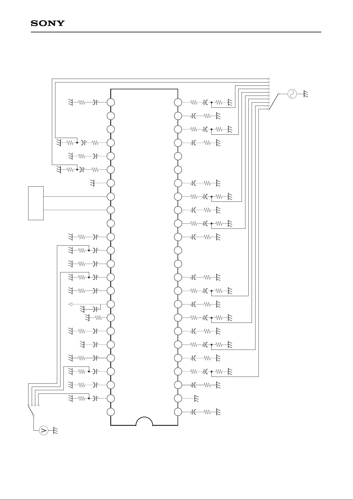
Signal is input from one of the following pins: 4, 6, 8, 10, 15, 17, 22, 24, 28 and 30.
Output signal is measured from one of the following pins: 36, 38, 45 and 47.
RV4
V4
LV4
S-3
S2-3
C3
BIAS
CIN1
LOUT1
VOUT1
ROUT1
TRAP
YIN1
MUTE
V
CC
VOUT2
ROUT2
YOUT2
LOUT2
COUT2
DC-OUT
SDA
SCL
ADR
YOUT1
GND
COUT1
LTV
TV
RTV
RV3
Y3
LV3
V3
S-2
S2-2
V1
LV1
Y1
RV1
C1
S2-1
S-1
V2
LV2
Y2
RV2
C2
10µ
10µ
1µ
0.47µ
1µ
0.47µ
1µ
0.47µ
1µ
0.1µ 0.47µ
1µ
0.47µ
1µ
0.1µ 0.47µ
1µ
0.47µ
1µ
10k 10k
600
75
600
75
600
75
600
75 75
600
75
600
75 75
600
10k
10µ
10k
10µ 0.1µ
75
10µ 0.47µ
75
1k
22µ
10µ
10k
10µ
10k
10µ
10k
10µ
10k
10µ
1µ
600
0.47µ
75
1µ
600
0.1µ
75
10µ
+9V
75
µ-COM
1
4
5
6
7
8
9
10
2
3
11
12
13
14
15
16
17
18
19
20
21
22
23
24
25
26
27
28
29
30
31
32
33
34
35
36
37
38
39
40
41
42
43
44
45
46
47
48
5.7k 5.7k 5.7k 5.7k 5.7k 5.7k 5.7k 5.7k
600
5.7k
5.7k
10k
10k
Input signal
Measurement point
Fig. 2-b. Audio system (gain, frequency response characteristics, total harmonic distortion, input dynamic range, cross talk) measurement circuit (CXA2089S)
Page 14
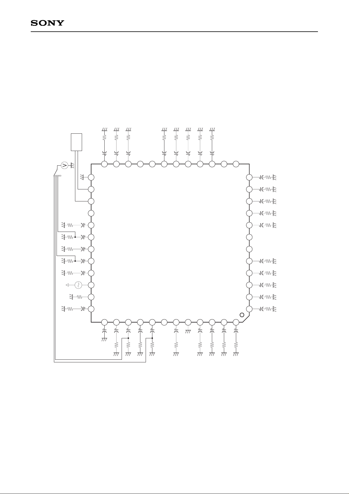
– 14 –
CXA2089Q/S
0.1µ
75
10µ
10k
1µ
0.47µ
600
75
600
10µ
10k
10µ
10µ
10k
0.1µ
0.47µ
75
1µ
0.47µ
1µ
75 75
0.1µ
0.47µ
75
1µ
0.47µ
1µ
75
0.47µ
1µ
0.47µ
1µ
0.1µ
10µ
1µ
0.47µ
1µ
75
600
75
600
75
600 60075600 600
75
10µ
600
600
10k
10k
0.47µ
75
1k
µ-com
10µ
10k
10µ
10k
10µ
10k
10µ
10k
10µ
10k
2
3
4
5
6
7
8
9
10
11
12
14
15
16
17
18
19
20
21
22
23
24
25
2627
28
29
30
35
34
31
32
33
40
39
38
37
41
42
43
44
45
46
47
48
1
BIAS
CIN1
LOUT1
VOUT1
ROUT1
TRAP1
YOUT1
GND
COUT1
LTV
TV
RTV
RV4
V4
LV4
S-3
S2-3
C3
RV3
Y3
LV3
V3
S-2
S2-2
YIN1
MUTE
V
CC
VOUT2
ROUT2
YOUT2
LOUT2
COUT2
DC OUT
SDA
SCL
ADR
V1
LV1
Y1
RV1
C1
S2-1
S-1
V2
LV2
Y2
RV2
C2
13
36
1µ
Input signal
Measurement point
Fig. 3-a. Audio system (ripple rejection ratio) measurement circuit (CXA2089Q)
A f=100Hz, 0.3Vp-p signal is applied to Vcc and the output signals from Pins 30, 32, 39 and 41 are measured.
Page 15
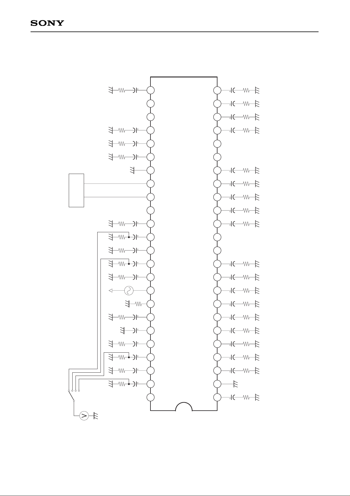
– 15 –
CXA2089Q/S
A f=100Hz, 0.3Vp-p signal is applied to Vcc and the output signals from Pins 36, 38, 45 and 47 are measured.
RV4
V4
LV4
S-3
S2-3
C3
BIAS
CIN1
LOUT1
VOUT1
ROUT1
TRAP
YIN1
MUTE
V
CC
VOUT2
ROUT2
YOUT2
LOUT2
COUT2
DC-OUT
SDA
SCL
ADR
YOUT1
GND
COUT1
LTV
TV
RTV
RV3
Y3
LV3
V3
S-2
S2-2
V1
LV1
Y1
RV1
C1
S2-1
S-1
V2
LV2
Y2
RV2
C2
10µ 10µ 1µ 0.47µ 1µ 0.47µ 1µ 0.47µ 1µ 0.1µ 0.47µ 1µ 0.47µ 1µ 0.1µ 0.47µ 1µ 0.47µ 1µ
10k 10k 600 75 600 75 600 75 600 75 75 600 75 600 75 600 75 600
10k
10µ
10k
10µ 0.1µ
75
10µ 0.47µ
75
1k
10µ
10k
10µ
10k
10µ
10k
10µ
10k
10µ
10k
1µ
600
0.47µ
75
1µ
600
0.1µ
75
10µ
+9V
75
µ-COM
1
4
5
6
7
8
9
10
2
3
11
12
13
14
15
16
17
18
19
20
21
22
23
24
25
26
27
28
29
30
31
32
33
34
35
36
37
38
39
40
41
42
43
44
45
46
47
48
10k
Input
signal
Measurement point
Fig. 3-b. Audio system (ripple rejection ratio) measurement circuit (CXA2089S)
Page 16
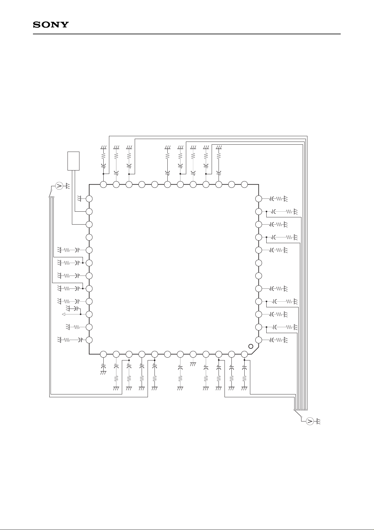
– 16 –
CXA2089Q/S
0.1µ
75
10µ
10k
1µ
0.47µ
600
75
600
10µ
10k
10µ
10µ
10k
0.1µ
0.47µ
75
1µ
0.47µ
1µ
75 75
0.1µ
0.47µ
75
1µ
0.47µ
1µ
75
0.47µ
1µ
0.47µ
1µ
0.1µ
10µ
1µ
0.47µ
1µ
75
600
75
600
75
600 600
75
600 600
75
10µ
600
600
10k
10k
0.47µ
75
22µ
1k
µ-com
10µ
10k
10µ
10µ
10k
10µ
10µ
10k
2
3
4
5
6
7
8
9
10
11
12
14
15
16
17
18
19
20
21
22
23
24
25
2627
28
29
30
35
34
31
32
33
40
39
38
37
41
42
43
44
45
46
47
48
1
BIAS
CIN1
LOUT1
VOUT1
ROUT1
TRAP1
YOUT1
GND
COUT1
LTV
TV
RTV
RV4
V4
LV4
S-3
S2-3
C3
RV3
Y3
LV3
V3
S-2
S2-2
YIN1
MUTE
V
CC
VOUT2
ROUT2
YOUT2
LOUT2
COUT2
DC OUT
SDA
SCL
ADR
V1
LV1
Y1
RV1
C1
S2-1
S-1
V2
LV2
Y2
RV2
C2
13
36
1µ
10k
10k
Measurement point
Measurement point
Fig. 4-a. Audio system (output DC offset voltage) measurement circuit (CXA2089Q)
Page 17
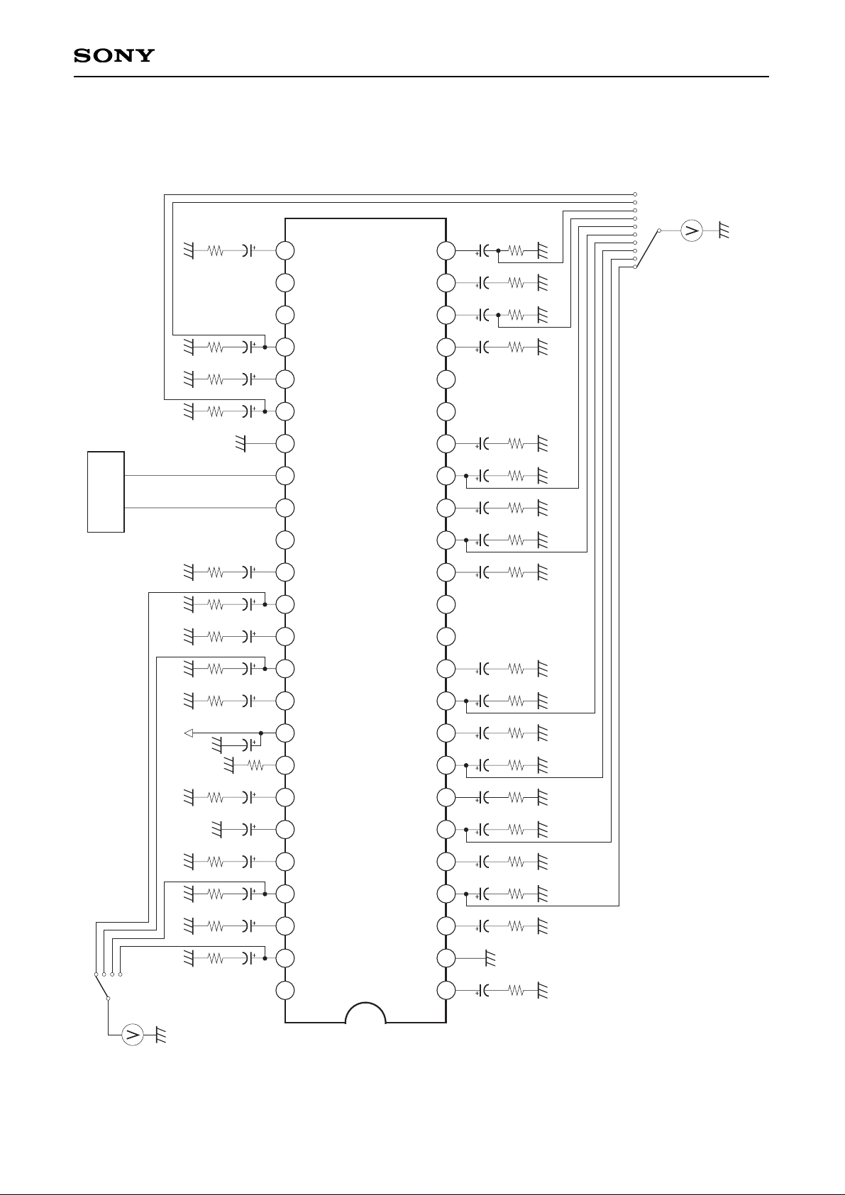
– 17 –
CXA2089Q/S
RV4
V4
LV4
S-3
S2-3
C3
BIAS
CIN1
LOUT1
VOUT1
ROUT1
TRAP
YIN1
MUTE
V
CC
VOUT2
ROUT2
YOUT2
LOUT2
COUT2
DC-OUT
SDA
SCL
ADR
YOUT1
GND
COUT1
LTV
TV
RTV
RV3
Y3
LV3
V3
S-2
S2-2
V1
LV1
Y1
RV1
C1
S2-1
S-1
V2
LV2
Y2
RV2
C2
10µ 10µ 1µ
0.47µ
1µ
0.47µ
1µ
0.47µ
1µ 0.1µ
0.47µ
1µ
0.47µ
1µ 0.1µ 0.47µ 1µ 0.47µ 1µ
10k 10k 600 75 600 75 600 75 600 75 75 600 75 600 75 75 600
10k
10µ
10k
10µ
0.1µ
75
10µ 0.47µ
1k
22µ
10µ
10k
10µ
10k
10µ
10k
10µ
10k
10µ
10k
1µ
600
0.47µ
75
1µ
0.1µ
75
10µ
+9V
75
µ-COM
1
4
5
6
7
8
9
10
2
3
11
12
13
14
15
16
17
18
19
20
21
22
23
24
25
26
27
28
29
30
31
32
33
34
35
36
37
38
39
40
41
42
43
44
45
46
47
48
600
600
10k 75
Measurement point
Measurement point
Fig. 4-b. Audio system (output DC offset voltage) measurement circuit (CXA2089S)
Page 18
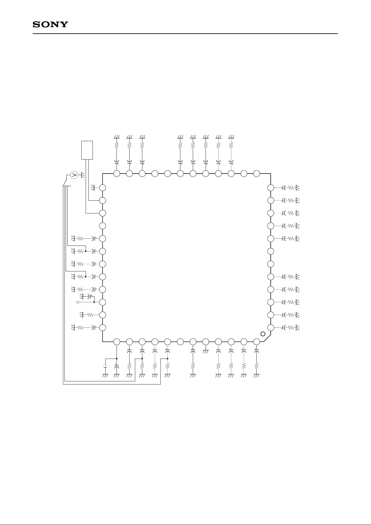
– 18 –
CXA2089Q/S
0.1µ
75
10µ
10k
1µ
0.47µ
600
75
600
10µ
10k
10µ
10µ
10k
0.1µ
0.47µ
75
1µ
0.47µ
1µ
75 75
0.1µ
0.47µ
75
1µ
0.47µ
1µ
75
0.47µ
1µ
0.47µ
1µ
0.1µ
10µ
1µ
0.47µ
1µ
75
600
75
600
75
600 600
75600 600
75
10µ
600
600
10k
10k
0.47µ
75
22µ
1k
Measurement point
µ-com
10µ
10k
10µ
10k
10µ
10k
10µ
10k
10µ
10k
2
3
4
5
6
7
8
9
10
11
12
14
15
16
17
18
19
20
21
22
23
24
25
2627
28
29
30
35
34
31
32
33
40
39
38
37
41
42
43
44
45
46
47
48
1
BIAS
CIN1
LOUT1
VOUT1
ROUT1
TRAP1
YOUT1
GND
COUT1
LTV
TV
RTV
RV4
V4
LV4
S-3
S2-3
C3
RV3
Y3
LV3
V3
S-2
S2-2
YIN1
MUTE
V
CC
VOUT2
ROUT2
YOUT2
LOUT2
COUT2
DC OUT
SDA
SCL
ADR
V1
LV1
Y1
RV1
C1
S2-1
S-1
V2
LV2
Y2
RV2
C2
13
36
1µ
4.5V
Fig. 5-a. Audio system (residual noise) measurement circuit (CXA2089Q)
Page 19
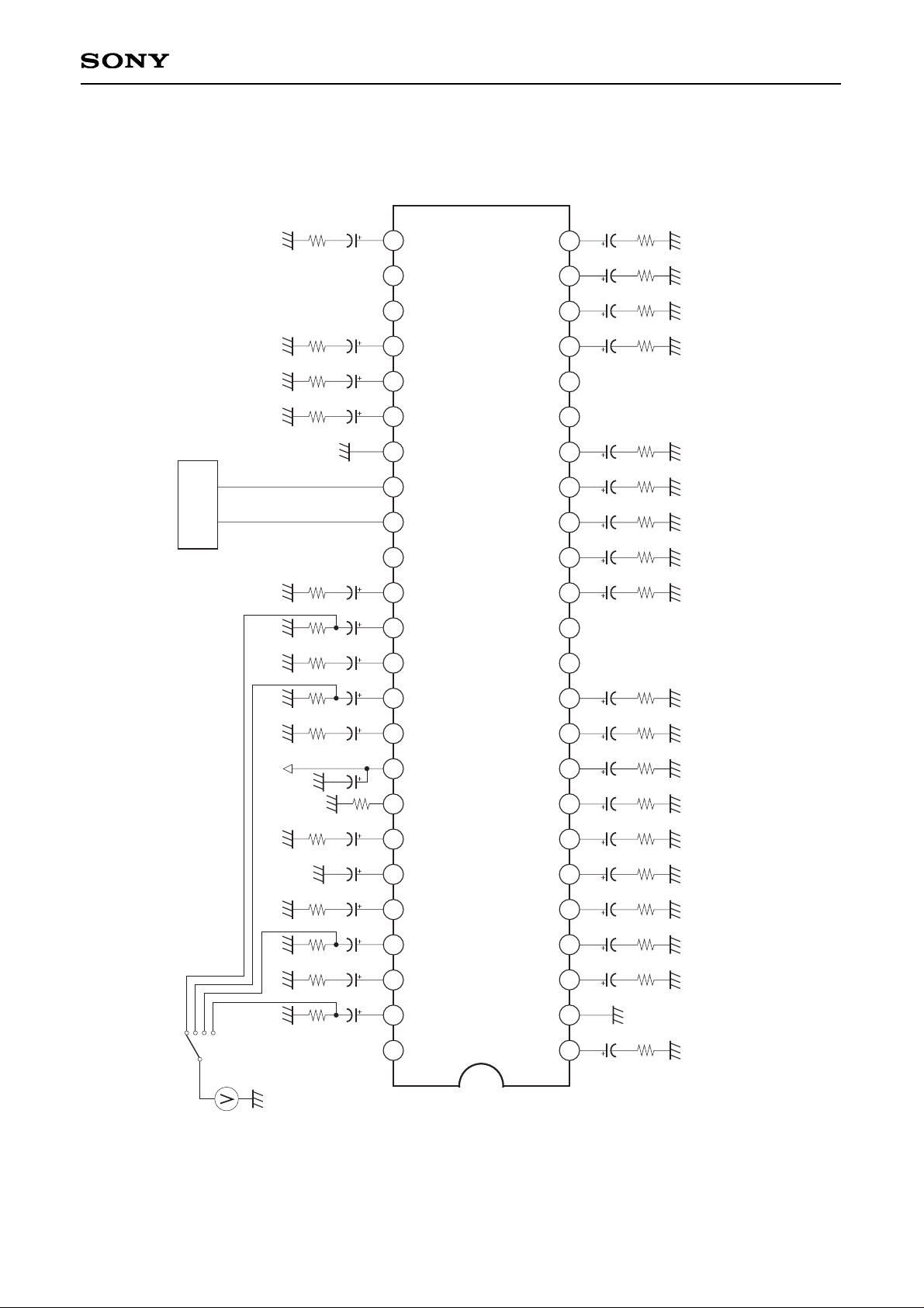
– 19 –
CXA2089Q/S
RV4
V4
LV4
S-3
S2-3
C3
BIAS
CIN1
LOUT1
VOUT1
ROUT1
TRAP
YIN1
MUTE
V
CC
VOUT2
ROUT2
YOUT2
LOUT2
COUT2
DC-OUT
SDA
SCL
ADR
YOUT1
GND
COUT1
LTV
TV
RTV
RV3
Y3
LV3
V3
S-2
S2-2
V1
LV1
Y1
RV1
C1
S2-1
S-1
V2
LV2
Y2
RV2
C2
10µ 10µ 1µ
0.47µ
1µ
0.47µ
1µ
0.47µ
1µ 0.1µ
0.47µ
1µ
0.47µ
1µ 0.1µ 0.47µ 1µ 0.47µ 1µ
10k 10k 600 75 600 75 600 75 600 75 75 600 75 600 75 75 600
10k
10µ
10k
10µ
0.1µ
75
10µ 0.47µ
1k
22µ
10µ
10k
10µ
10k
10µ
10k
10µ
10k
10µ
10k
1µ
600
0.47µ
75
1µ 0.1µ
75
10µ
+9V
75
µ-COM
1
4
5
6
7
8
9
10
2
3
11
12
13
14
15
16
17
18
19
20
21
22
23
24
25
26
27
28
29
30
31
32
33
34
35
36
37
38
39
40
41
42
43
44
45
46
47
48
600
600
10k 75
Measurement point
Fig. 5-B. Audio system (residual noise) measurement circuit (CXA2089S)
Page 20
– 20 –
CXA2089Q/S
I2C BUS Control Signal
tSU;STO
34
33
tSU;STA
S P
tHIGH tF tSU;DATtLOW tR
tHD;DAT
SP
tHD;STA
tBUF
SCL
SDA
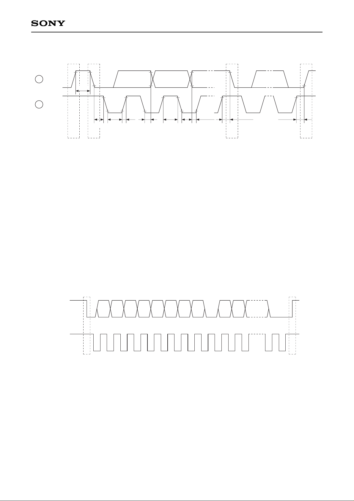
Fig. 6. I2C BUS Control Signal Timing Chart
Description of Operation
The CXA2089Q/S is a TV I2C bus-compatible AV switch IC. The video system and the stereo audio system
both have 5 inputs and 2 outputs each. 3 of the 5 video system inputs support S2 and S protocols.
The desired inputs can be independently assigned to each output (in the audio system, the left and right
channels are processed as one unit) by I2C bus control. However, the same input is assigned to both the video
and audio system output 2.
I2C BUS Registers
1) I2C BUS
The I2C bus (inter-IC bus) is an inter-IC bus system developed by Philips. Two lines (SDA – serial data, SCL –
serial clock) provide control over start, stop, data transfer, synchronization, and collision avoidance. The IC
outputs are either open collector or open drain, forming a bus line in the wired OR format.
SCL
SDA
S P
MSB LSB
A
MSB LSB
A
921987654321
S: Start condition; SDA is set "Low" when SCL is "High"
P: Stop condition; SDA is set "High" when SCL is "High"
A: Acknowledge; signal sent from the slave
Data is transmitted by MSB-first. One data unit consists of 8 bits, to which the acknowledge signal, which
indicates that the data has been accepted by the slave, is attached at the end. Normally, the slave∗1IC
receives data at the rising edge of SCL and the master∗2IC changes data at the falling edge of SCL.
∗1
Slave: An IC that is placed under the control of the master. In a normal system, all devices excluding the
central microcomputer are slaves.
∗2
Master: A central microcomputer or other controlling IC.
Page 21
– 21 –
CXA2089Q/S
2) Control Registers
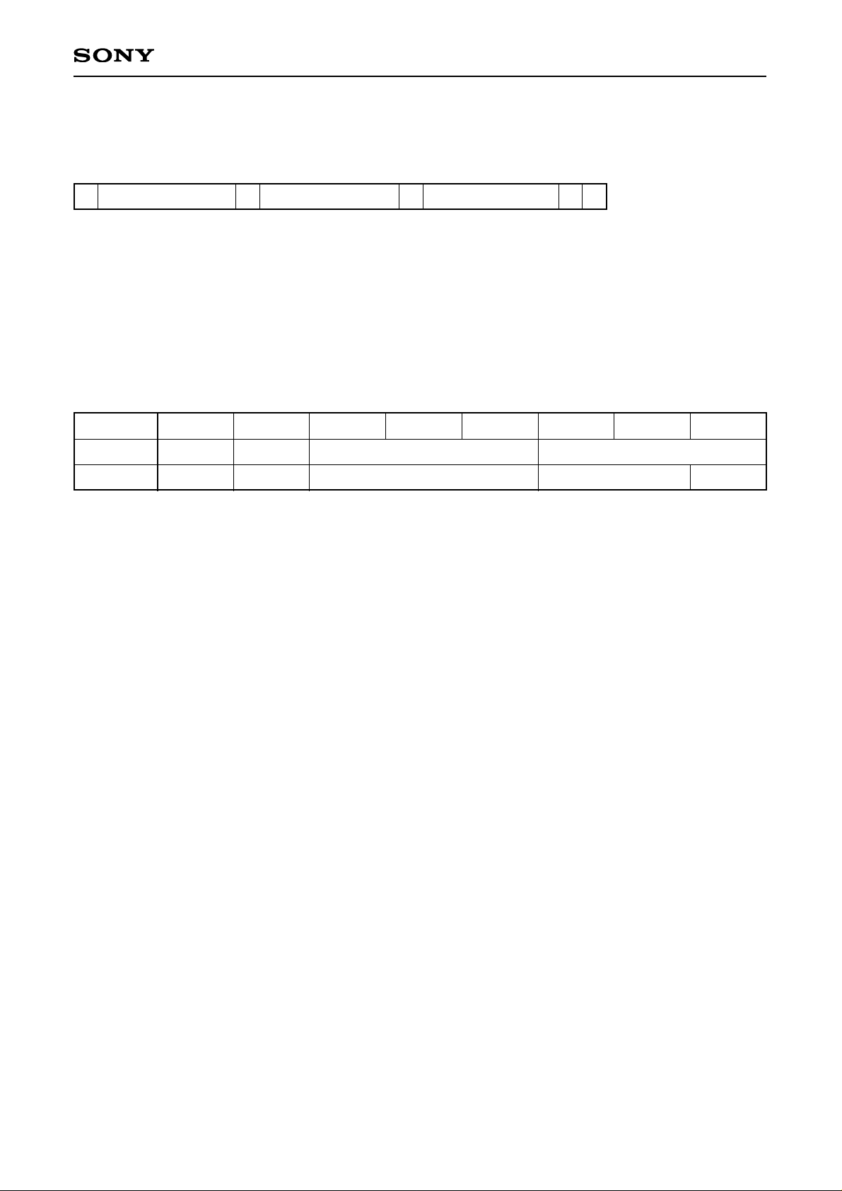
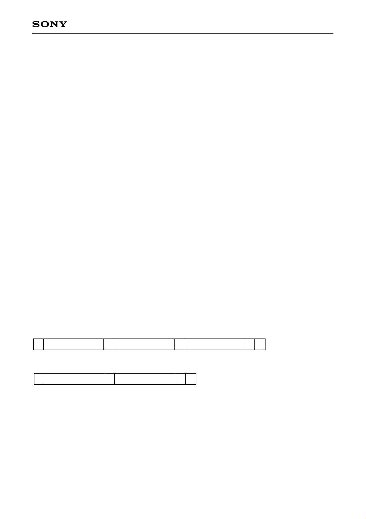
The CXA2089Q/S control is exercised by writing 2-byte data into the two 8-bit control registers which control
the output selector circuits for the 2 outputs.
S
Slave address
A DATA1 A DATA2 A P
S: Start condition
A: Acknowledge
P: Stop condition
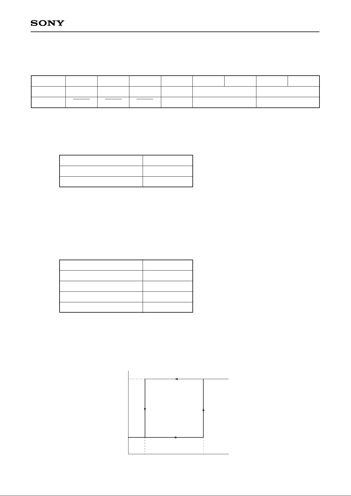
Control register structure (DATA1 and DATA2)
• All registers are set to "0" during IC power on.
• "∗" indicates undefined.
Slave add.
DATA1
DATA2
1
A-GAIN
∗
0
S/COMP1
S/COMP2
0
V-IN1
AV-IN2
1 0 0
DC OUT
ADR
A-IN1
R/W
b7 b6 b5 b4 b3 b2 b1 b0
∗
R/W (1): Read/write mode
0: Control data write
1: Status register read
ADR (1): This bit sets the slave address set by the address pin.
0: 90H
1: 92H
A-GAIN (1): LOUT1/ROUT1 output gain selector
0: 0dB output
1: –6dB output
S/COMP1 and S/COMP2 (1 each): S terminal input/composite signal input selectors
By setting S/COMP1 to "0", when composite signal input is selected, YOUT1/COUT1 output the
inputs from YIN1/CIN1.
0: Composite signal inputs (TV, V1 to V4 inputs)
1: S terminal inputs (Y1/C1 to Y3/C3 inputs)
V-IN1 (3 each): This bit selects the input signals output to each video output.
0: Mute
1: Selects the TV input
2: Selects the V1 and Y1/C1 inputs
3: Selects the V2 and Y2/C2 inputs
4: Selects the V3 and Y3/C3 inputs
5: Selects the V4 inputs
6: Mute
7: Mute
Page 22
– 22 –
CXA2089Q/S
A-IN1 (3 each): This bit selects the input signals output to each audio output.
0: Mute
1: Selects the LTV/RTV inputs
2: Selects the LV1/RV1 inputs
3: Selects the LV2/RV2 inputs
4: Selects the LV3/RV3 inputs
5: Selects the LV4/RV4 inputs
6: Mute
7: Mute
AV-IN2 (3): This bit selects the input signals output to output 2 (VOUT2, YOUT2/COUT2, LOUT2/ROUT2).
Note) Both the video output and the audio output are selected at the same time only for AV-IN2.
0: Mute
1: Selects the TV and LTV/RTV inputs
2: Selects the V1, Y1/C1 and LV1/RV1 inputs
3: Selects the V2, Y2/C2 and LV2/RV2 inputs
4: Selects the V3, Y3/C3 and LV3/RV3 inputs
5: Selects the V4 and LV4/RV4 inputs
6: Mute
7: Mute
DC OUT (2): This bit sets the DC voltage output from DC OUT.
0: 4.5V
1: 0V
2: 1.9V
3: 4.5V
3) Status Registers
• When reading two bytes
S
Slave address
A DATA1 A DATA2 NA P
S: Start condition
A: Acknowledge
NA: No acknowledge
P: Stop condition
• When reading one byte
S
Slave address
A DATA1 NA P
When communication is to be terminated in the status register reading mode, the no-acknowledge signal is
needed to assure that the master does not issue the acknowledge signal to the slave.
It is possible to read only DATA1 of the status register by sending the no-acknowledge signal after DATA1.
Page 23
– 23 –
CXA2089Q/S
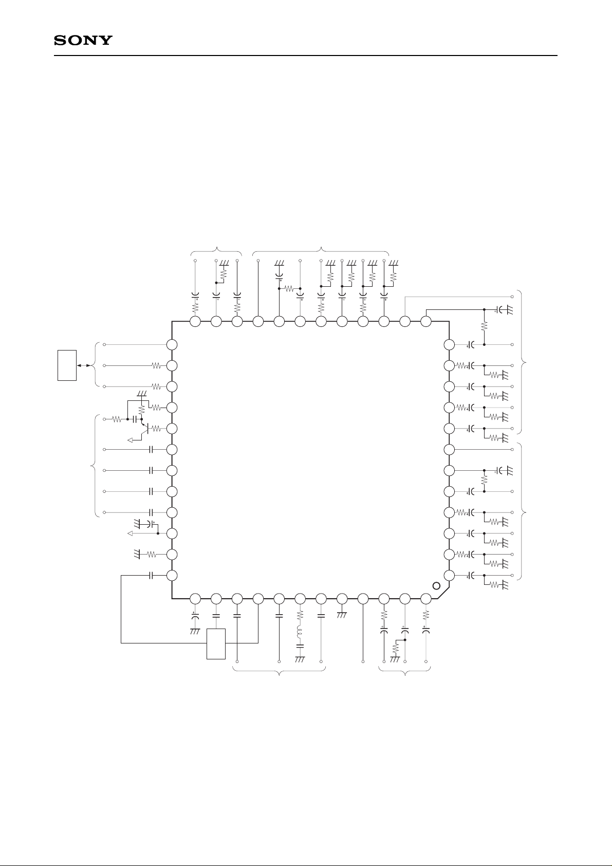
S-C1, S-C2, S-C3 (2 each): S2-1, S2-2 and S2-3 pin status
0: 4:3 video signal
1: 4:3 letter-box signal
2: 16:9 video squeezed signal
3: No signal
S-C1 to S-C3 are actually determined by comparing the S2-1 to S2-3 pin DC voltages with two
threshold. However, when the S-1 to S-3 pins are open, the outputs are fixed to "3".
S2-1 to S2-3 pin DC voltage S-C1 to S-C3
1.3V or less
1.3V or more to 2.5V or less
2.5V or more
S-1 to S-3 OPEN
0
1
2
3
Status register structure (DATA1 and DATA2)
"∗" indicates undefined.
Slave add.
DATA1
DATA2
1
S1SEL
S1SEL
0
S2SEL
S2SEL
S3SEL
S3SEL
∗
∗
0 1 0 0
S-C1
S-C3
ADR
S-C2
∗
1
b7 b6 b5 b4 b3 b2 b1 b0
S1SEL to S3SEL (1 each): S-1 to S-3 pin status
0: S-1 to S-3 pins are not grounded.
1: S-1 to S-3 pins are grounded.
S1SEL to S3SEL are actually determined by comparing the S-1 to S-3 pin DC voltages with 3.5V.
S-1 to S-3 pin DC voltage S1SEL to S3SEL
3.5V or more
3.5V or less
0
1
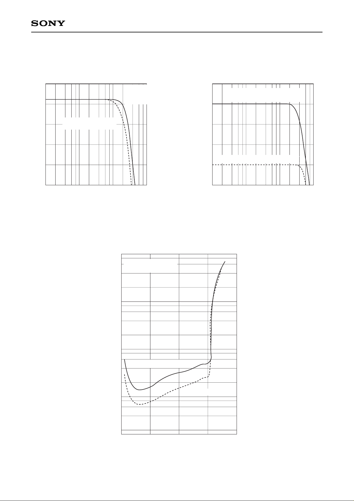
4) Power-on Reset
The CXA2089Q/S has an internal power-on reset function that sets each control register to "0" during IC power
ON.
The power-on reset VTH has hysteresis.
Power-on reset
released
Power-on reset
4.5V 5.6V
VCC
Page 24
– 24 –
CXA2089Q/S
1µ
0.47µ
1µ
COMB
FILTER
0.47µ
470k
75
1µ
0.47µ
470k
1µ
75
0.1µ
1µ
75
0.1µ0.47µ
470k
75
1µ
0.47µ
470k
1µ
75
2
3
4
5
6
7
8
9
10
11
12
14
15
16
17
18
19
20
21
22
23
24
25
26
2728
29
30
35
34
31
32
33
40
39
38
37
41
42
43
44
45
46
47
48
1
BIAS
CIN1
LOUT1
VOUT1
ROUT1
TRAP1
YOUT1
GND
COUT1
LTV
TV
RTV
RV4
V4
LV4
S-3
S2-3
C3
RV3
Y3
LV3
V3
S-2
S2-2
YIN1
MUTE
V
CC
VOUT2
ROUT2
YOUT2
LOUT2
COUT2
DC OUT
SDA
SCL
ADR
V1
LV1
Y1
RV1
C1
S2-1
S-1
V2
LV2
Y2
RV2
C2
1µ
75
0.47µ
1µ
0.47µ
1µ
0.1µ
1µ
620
180µ
0.1µ
4.7k
75
220
22µ
1k0.47µ
10p
1µ
0.47µ
1µ
13
36
75
470k
75
470k
0.1µ
10µ
220
µ-com
75
10µ 10µ 10µ 10µ
10µ
10µ
10µ
1.2k
1.2k
75
1.2k 1.2k 1.2k 1.2k
1.2k
1.2k
1.2k
1.2k
75
VIDEO 1 input VIDEO 2 input
VIDEO 3 input
VIDEO 2 output
VIDEO 1 output
TV input
VIDEO 4 input
Application Circuit (CXA2089Q)
• Depending on the output bias of the comb filters, pay
attention to the polarities of the capacitors since the
bias at Pins 36 and 38 is approximately 3.1V and
4.5V, respectively.
• Connect Pin 25 to Vcc when setting the slave address
of the IC to 92H.
• The audio output can be muted by setting Pin 35 to
3.5V or more.
• The TRAP (Pin 42) are of 3.58MHz subcarrier.
• Pay attention to the polarities of the capacitors since
each output of video system and audio system has
optional bias, respectively.
Application circuits shown are typical examples illustrating the operation of the devices. Sony cannot assume responsibility for
any problems arising out of the use of these circuits or for any infringement of third party patent and other right due to same.
Page 25

– 25 –
CXA2089Q/S
RV4
V4
LV4
S-3
S2-3
C3
BIAS
CIN1
LOUT1
VOUT1
ROUT1
TRAP
YIN1
MUTE
V
CC
VOUT2
ROUT2
YOUT2
LOUT2
COUT2
DC-OUT
SDA
SCL
ADR
YOUT1
GND
COUT1
LTV
TV
RTV
RV3
Y3
LV3
V3
S-2
S2-2
V1
LV1
Y1
RV1
C1
S2-1
S-1
V2
LV2
Y2
RV2
C2
10µ 10µ
1µ
0.47µ 0.47µ 0.1µ 0.47µ1.2k
75
75
0.1µ 10µ 0.47µ
1k
22µ
10µ 10µ 10µ 10µ 0.47µ
1µ
1.2k
0.1µ
+9V
µ-COM
1µ
1.2k
75
1µ
1.2k
470k
0.47µ
75
1.2k
470k
1µ
75
0.1µ
75
1µ
1.2k
470k
0.47µ
75
1.2k
470k
1µ
0.47µ
75
1µ
1.2k
470k
0.47µ
75
1.2k
470k
1µ
75
1.2k
1µ
75
4.7k
0.1µ
220 220
COMB
FILTER
620
10µ
10µ
10p
180µ
25
26
27
28
29
30
31
32
33
34
35
36
37
38
39
40
41
42
43
44
45
46
47
48
1
4
5
6
7
8
9
10
2
3
11
12
13
14
15
16
17
18
19
20
21
22
23
24
Video1 output Video2 output
75
Video4 input
Video1 input Video2 input Video3 inputTV input
1µ 1µ 1µ
Application Circuit (CXA2089S)
• Depending on the output bias of the comb filters, pay attention to the polarities of the capacitors
since the bias at Pins 42 and 44 is approximately 3.1V and 4.5V, respectively.
• Connect Pin 31 to Vcc when setting the slave address of the IC to 92H.
• The audio output can be muted by setting Pin 41 to 3.5V or more.
• The TRAP (Pin 48) are of 3.58MHz subcarrier.
• Pay attention to the polarities of the capacitors since each output of video system and audio
system has optional bias, respectively.
Application circuits shown are typical examples illustrating the operation
of the devices. Sony cannot assume responsibility for any problems
arising out of the use of these circuits or for any infringement of third
party patent and other right due to same.
Page 26
– 26 –
CXA2089Q/S
Example of Representative Characteristics
Video system frequency response characteristics
100k
–2
Frequency [Hz]
1M 10M 100M
0
2
4
6
8
Video system input/output gain [dB]
Y1/C1 to Y3/C3
→ VOUT1, VOUT2
TV, V1 to V4 → VOUT1, VOUT2
Y1 to Y3 → YOUT1, YOUT2
C1 to C3 → COUT1, COUT2
1k
Audio system frequency response characteristics
–8
Frequency [Hz]
10k 100k 1M
–6
–4
–2
0
2
Audio system input/output gain [dB]
L/RTV, L/R1 to L/R4 → LOUT1 (0dB)
L/RTV, L/R1 to L/R4 → LOUT2
0
Audio system distortion vs. Input amplitude
0.002
Input amplitude [Vrms]
1 2 4
0.01
0.1
1
10
Total harmonic distortion [%]
LOUT1 output (0dB gain)
f = 1kHz
400Hz HPF, 80kHz LPF
3
L/RTV, L/R1 to L/R4 → LOUT1 (–6dB)
LOUT2 output
Page 27
– 27 –
CXA2089Q/S
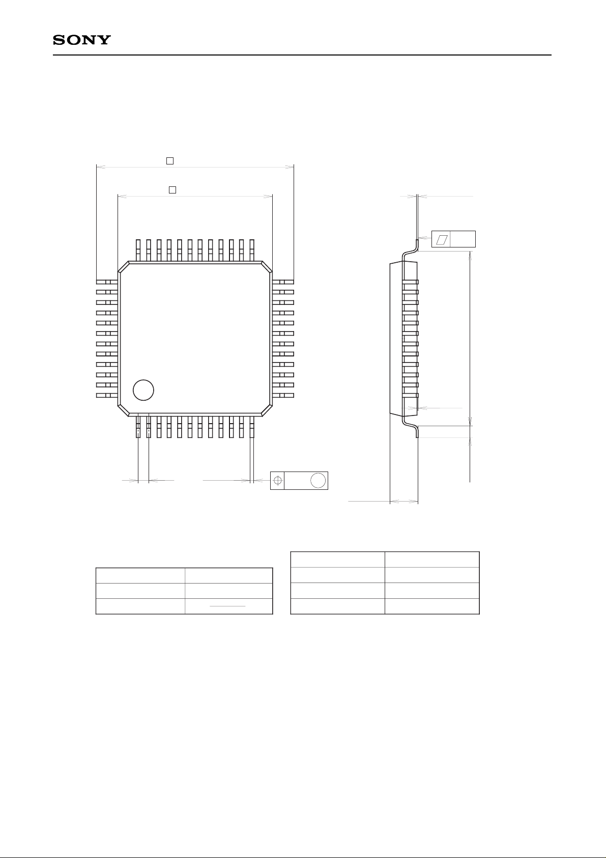
Package Outline Unit: mm
CXA2089Q
SONY CODE
EIAJ CODE
JEDEC CODE
M
PACKAGE STRUCTURE
PACKAGE MATERIAL
LEAD TREATMENT
LEAD MATERIAL
PACKAGE WEIGHT
EPOXY RESIN
SOLDER / PALLADIUM
PLATING
COPPER / 42 ALLOY
48PIN QFP (PLASTIC)
15.3 ± 0.4
12.0 – 0.1
+ 0.4
0.8 0.3 – 0.1
+ 0.15
± 0.12
13
24
2536
37
48
1 12
2.2 – 0.15
+ 0.35
0.9 ± 0.2
0.1 – 0.1
+ 0.2
13.5
0.15
0.15 – 0.05
+ 0.1
QFP-48P-L04
∗QFP048-P-1212-B
0.7g
NOTE : PALLADIUM PLATING
This product uses S-PdPPF (Sony Spec.-Palladium Pre-Plated Lead Frame).
Page 28
– 28 –
CXA2089Q/S
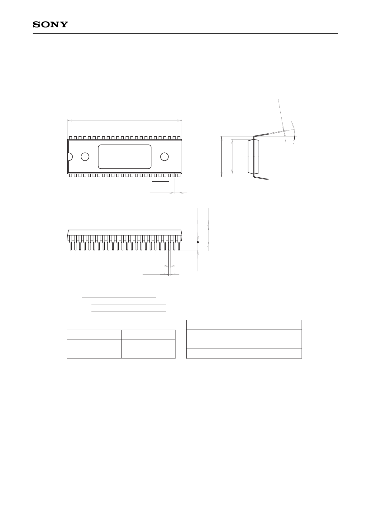
CXA2089S
48PIN SDIP (PLASTIC)
13.0
+ 0.3
– 0.1
4.6
+ 0.4
– 0.1
0.25
+ 0.1
– 0.05
48 25
1 24
1.778
15.24
0° to 15°
0.5 ± 0.1
0.9 ± 0.15
3.0 MIN 0.5 MIN
SONY CODE
EIAJ CODE
JEDEC CODE
PACKAGE STRUCTURE
PACKAGE MATERIAL
LEAD TREATMENT
LEAD MATERIAL
PACKAGE MASS
EPOXY RESIN
PLATING
42/COPPER ALLOY
5.1g
SDIP-48P-02
SDIP048-P-0600
43.2
+ 0.4
– 0.1
SOLDER/PALLADIUM
1.All mat surface type.
Two kinds of package surface:
2.Center part is mirror surface.
 Loading...