

Page 1
—1—
E99857
Sony reserves the right to change products and specifications without prior notice. This information does not convey any license by
any implication or otherwise under any patents or other right. Application circuits shown, if any, are typical examples illustrating the
operation of the devices. Sony cannot assume responsibility for any problems arising out of the use of these circuits.
Absolute Maximum Ratings (Ta=25 °C, GND=0 V)
• Supply voltage VCC/R/G/B 14 V
VCC 7V
• Operating temperature Topr –20 to +75 °C
• Storage temperature Tstg –65 to +150 °C
• Allowable power dissipation
PD 2.05 W
Recommended Operating Conditions
Supply voltage VCC/R/G/B 12±0.5 V
VCC 5±0.5 V
Description
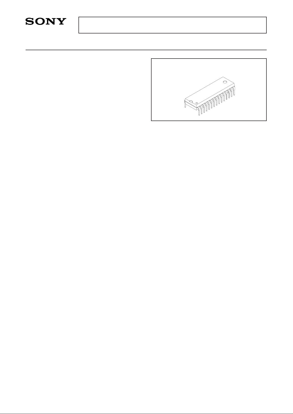
The CXA2067AS is a bipolar IC developed for
high-resolution computer displays.
Features
• Wide-band amplifier: 170 MHz@–3 dB (Typ)
• Input dynamic range: 1.0 Vp-p (typ)
• High gain preamplifier (17 dB)
• R, G and B in a single package (SDIP 30 pins)
• I2C bus control
Contrast control
Sub contrast control
Brightness control
OSD contrast control
Cut-off control: 4 channels of DAC output
2 blanking level modes
(0.5 V fixed, pedestal –0.3 V)
• Sync separator for sync-on-green
• Blanking mixing function
• OSC mixing function
• Video interval detection function
• VBLK sync DAC refresh system
• 12 V power supply interlocked power saving
function
Applications
High-resolution computer displays
Structure
Bipolar silicon monolithic IC
Preamplifier for High-Resolution Computer Display
30 pin SDIP (Plastic)
CXA2067AS
Page 2
—2—
CXA2067AS
LPF
SDA
SCL
COF R
COF G
COF B
COF RGB
RIN
V
CC
GIN
SYNC IN
BIN
CLP
OSD-R
OSD-G
OSD-B
CSYNC/VDET
V
CC R
S/H-R
ROUT
GND-R
S/H-G
GOUT
GND-G
V
CC G
S/H-B
BOUT
GND-B
BLKING
YS
V
CC B
to
OSDSW
to
OSDSW
to
OSDSW
to
OSDSW
Rch
Bch
OSD YS
GENERATOR
GAIN
CONTROL
AMP
GAIN CONTROL DATA
SYNC SEP/VDET
VDET
COMPARATOR
SYNC
SEPARATOR
SVSW
SUB
CONTRAST
CONTRAST
OSD SW
BLANKING
MODE
BLANKING PULSE
BRIGHTNESS
OSD GAIN (R)
OSD PULSE (13PIN)
YS PULSE (17PIN)
To each MODE SW
I C BUS
DECORDER
2
BLANKING
BUFFER AMP
Same as R channel
Same as R channel
Gch
17
18
19
20
21
23
24
25
26
27
28
29
30
1
2
3
4
5
6
7
8
9
10
11
12
13
14
15
12V
5V
12V
12V
22
16
D/A CONVERTOR
CONTRAST
SUB CONTRAST (R)
SUB CONTRAST (G)
SUB CONTRAST (B)
OSD GAIN (R)
OSD GAIN (G)
OSD GAIN (B)
BRIGHTNESS (RGB)
CUTOFF (R)
CUTOFF (G)
CUTOFF (B)
CUTOFF (RGB)
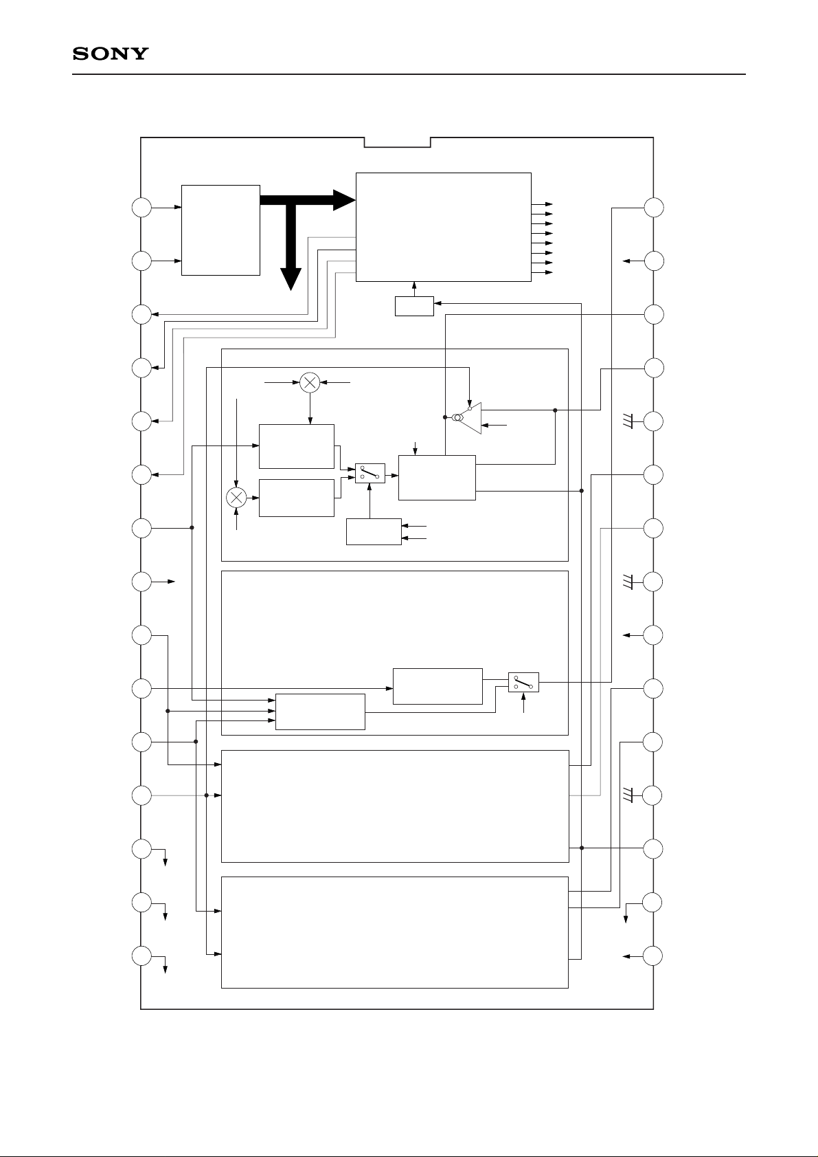
Block Diagram
Page 3
—3—
CXA2067AS
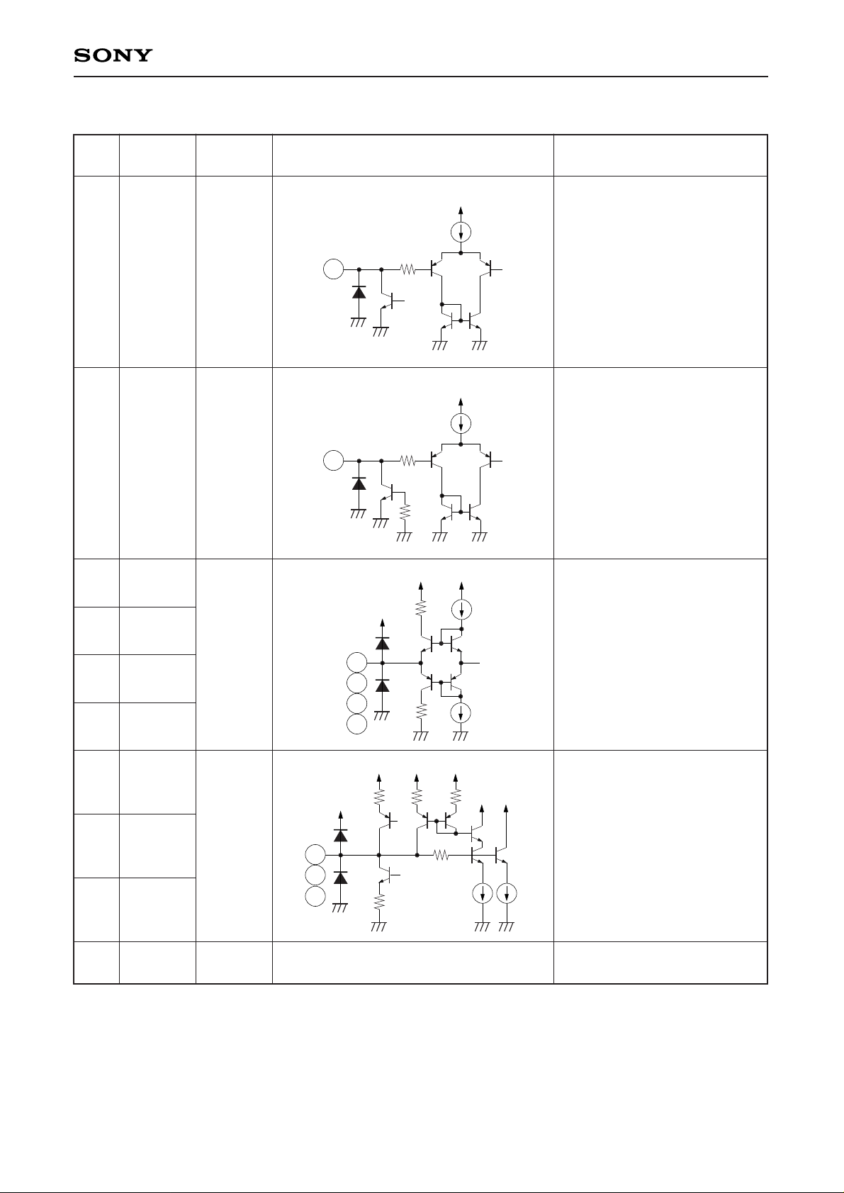
Pin Description
1
2
3
4
5
6
7
9
11
8
SDA
SCL
COF R
COF G
COF B
COF RGB
RIN
GIN
BIN
VCC
—
—
—
1.8 V
(Clamp)
5 V
1
4k
VCC
4k
10k
VCC
2
100
VCC
VCC
3
4
5
6
VCC
1k
1k
VCC
VCC
VCC VCC
14k
V
CC
8k
V
CC
7
9
300
11
I2C bus standard SDA
(serial data) input/output.
VILMAX=1.5 V
VIHMIN=3.5 V
VOLMAX=0.4 V
I2C bus standard SCL
(serial clock) input/output.
VILMAX=1.5 V
VIHMIN=3.5 V
DAC output for cut-off
adjustment.
Output DC is 1 to 4 V.
R, G and B signal inputs.
Input via a capacitor.
5 V power supply.
Pin
Symbol
Pin
Equivalent circuit Description
No. voltage
Page 4
—4—
CXA2067AS
10
12
13
14
15
16
17
SYNC IN
CLP
OSD-R
OSD-G
OSD-B
VCC B
YS
2.8 V
—
—
12 V
—
100
VCC
VCC
VCC
150
10
VCC
VCC
10k
2p
10k10k
12
VCC
VCC
10k
2p
13
14
15
5k
VCC
VCC
10k
2p
5k
17
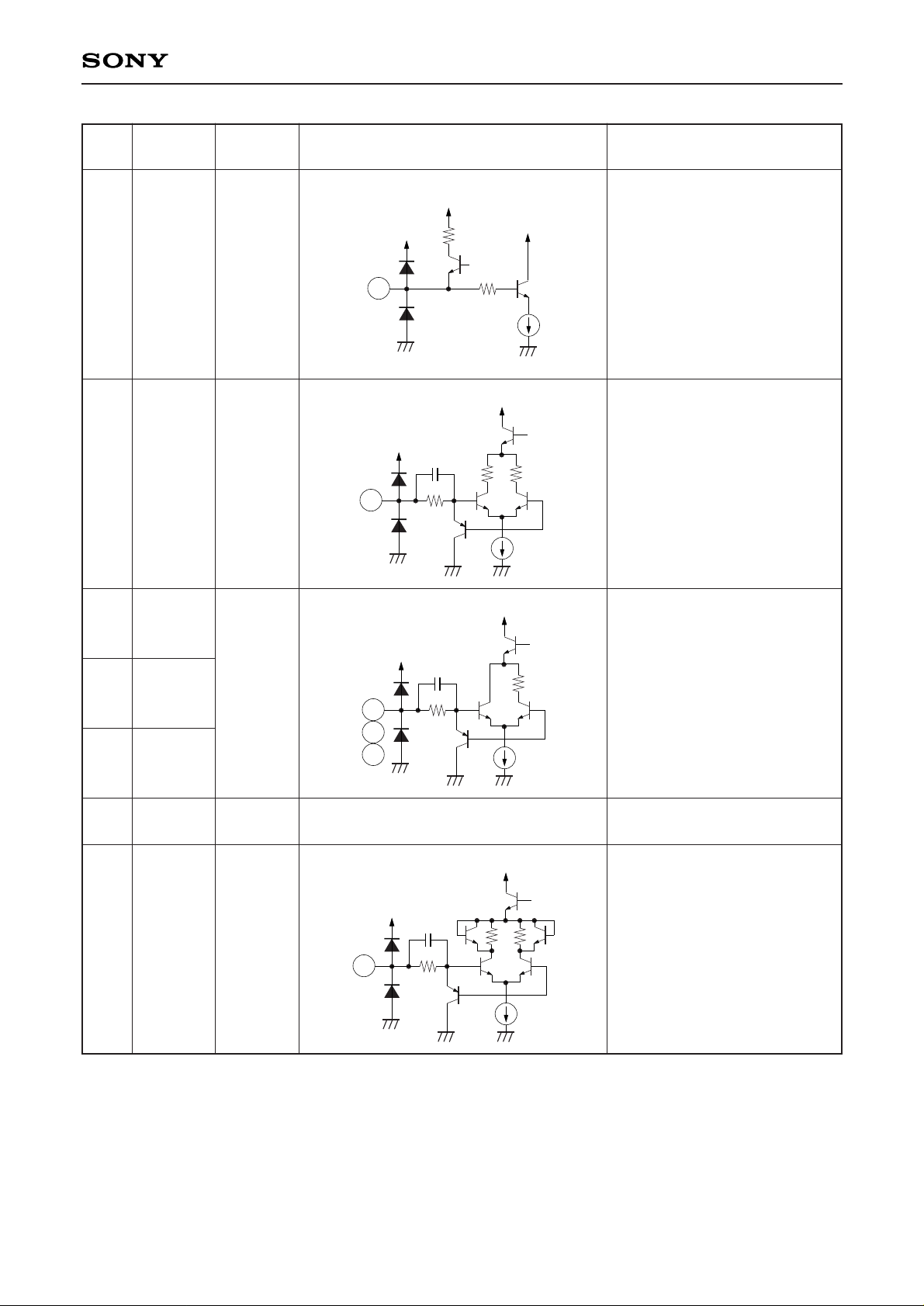
Sync-on-green signal input.
Input via a capacitor.
Clamp pulse (positive polarity)
input.
VILMAX=0.8 V
VIHMIN=2.8 V
OSD control inputs.
VILMAX=0.8 V
VIHMIN=2.8 V
12 V power supply. (B channel)
YS (OSD BLK) control input.
VILMAX=0.8 V
VIHMIN=2.8 V
Pin
Symbol
Pin
Equivalent circuit Description
No. voltage
Page 5
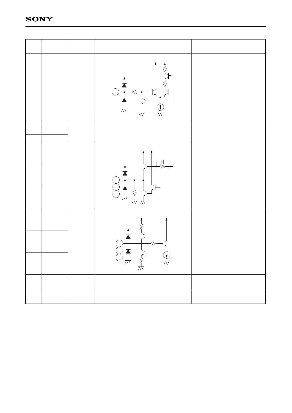
—5—
CXA2067AS
18
19
23
26
20
24
27
21
25
28
22
29
BLKING
GND-B
GND-G
GND-R
BOUT
GOUT
ROUT
S/H-B
S/H-G
S/H-R
VCC G
VCC R
—
0 V
—
—
12 V
12 V
VCC VCC
VCC
10k
30k
4k
18
VCCR/G/B
2p
310
5k
20
24
27
VCCR/G/B VCCR/G/B
1k
VCC
VCC
VCC
1k
300
21
25
28
Blanking pulse input.
Set the V blanking pulse width
to 300 µs or more.
VILMAX=0.8 V
VIHMIN=2.8 V
Ground.
R, G and B outputs.
Brightness sample-and-hold.
Connect to GND via a capacitor.
12 V power supply. (G channel)
12 V power supply. (R channel)
Pin
Symbol
Pin
Equivalent circuit Description
No. voltage
Page 6
—6—
CXA2067AS
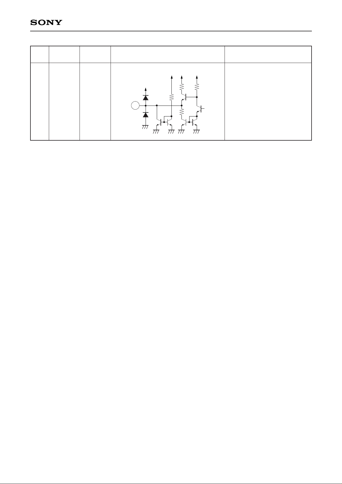
30
CSYNC
/VDET
—
VCC VCC
VCC
500
100
VCC
5k
20k
30
Sync-on-green signal sync
separator output/video detector
output.
Either of them is selected by
SVSW of I2C bus.
Typ. : High=4.3 V
Low=0.2 V
(positive polarity)
Pin
Symbol
Pin
Equivalent circuit Description
No. voltage
Page 7

—7—
CXA2067AS
Definitions of I2C Bus Register
Slave Address
SLAVE RECEIVER : 40 (HEX)
Register Table
SUB ADDRESS
00h
01h
02h
03h
04h
05h
06h
07h
08h
09h
0Ah
BIT7 BIT6 BIT5 BIT4 BIT3 BIT2 BIT1 BIT0
CONTRAST
0 BLK MODE BRIGHTNESS
CUT OFF R
CUT OFF G
CUT OFF B
VDET LEVEL OSD GAIN
CUT OFF RGB
SUB CONTRAST R
SUB CONTRAST G
SUB CONTRAST B
VDET OFF SVSW ∗ ∗ ∗ ∗ ∗ VSOFF
Note) ∗: don’t care
Sub Address CONTRAST (8): Performs the gain control for R, G and B channels in common.
0000 Control is performed by the multiplication with SUB CONTRAST. The white
balance is adjusted by SUB CONTRAST and the luminance is adjusted by
CONTRAST.
0 : Gain minimum (–30 dB or less)
255 : Gain maximum (+17 dB)
Sub Address BLK MODE (1): Switches the blanking level.
0001 0 : Pedestal–0.3 V
1 : 0.3 V fixed
Sub Address BRIGHTNESS (6): Performs the black level control for R, G and B channels in common.
0001 0 : Black level minimum (0.9 V)
63 : Black level maximum (2.8 V)
Sub Address CUT OFF R (8): Performs the Pin 3 (COF R) output voltage control.
0010 0 : Output voltage minimum (1 V)
255 : Output voltage maximum (4 V)
Sub Address CUT OFF G (8): Performs the Pin 4 (COF G) output voltage control.
0011 0 : Output voltage minimum (1 V)
255 : Output voltage maximum (4 V)
Sub Address CUT OFF B (8): Performs the Pin 5 (COF B) output voltage control.
0100 0 : Output voltage minimum (1 V)
255 : Output voltage maximum (4 V)
Page 8

—8—
CXA2067AS
Sub Address VDET LEVEL (2): Controls the signal detection (VDET) slice level.
0101 0 : Slice level minimum (RIN or GIN or BIN=30 mV)
1 : Slice level maximum (RIN or GIN or BIN=220 mV)
Sub Address OSD GAIN (6): Performs the OSD gain control for R, G and B channels in common.
0110 Control is performed by the multiplication with SUB CONTRAST (upper 6
bits) so that the video white balance and tracking are obtained.
0 : Gain minimum (0 Vp-p)
63 : Gain maximum (5 Vp-p)
Sub Address CUT OFF RGB (8): Performs the Pin 6 (COF RGB) output voltage.
0110 0 : Output voltage minimum (1 V)
255 : Output voltage maximum (4 V)
Sub Address SUB CONTRAST R (8): Performs the R channel gain control.
0111 Control is performed by the multiplication with CONTRAST. Use for
the white balance adjustment.
0 : Gain minimum (–30 dB or less)
255 : Gain maximum (+17 dB)
Sub Address SUB CONTRAST G (8): Performs the G channel gain control.
1000 Control is performed by the multiplication with CONTRAST. Use for
the white balance adjustment.
0 : Gain minimum (–30 dB or less)
255 : Gain maximum (+17 dB)
Sub Address SUB CONTRAST B (8): Performs the B channel gain control.
1001 Control is performed by the multiplication with CONTRAST. Use for
the white balance adjustment.
0 : Gain minimum (–30 dB or less)
255 : Gain maximum (+17 dB)
Sub Address VDET OFF (1): Performs the Pin 30 output control.
1010 0 : Output ON
1 : Output OFF
Sub Address SV SW (1): Switches the Pin 30 output signal (sync separator/video detector).
1010 0 : Sync separator output
1 : Video detector output
Sub Address VS OFF (1): Performs the control of VBLK sync DAC refresh function.
1010 0 : Function operation ON
1 : Function operation OFF
Page 9

—9—
CXA2067AS
I2C Bus Logic System
No.
1
2
3
4
5
6
7
8
9
10
11
12
13
14
Item
High level input voltage
Low level input voltage
Low level output voltage with 3 mA
SDA current inflow
Maximum clock frequency
Minimum waiting time for data change
Minimum waiting time for data
transmission start
Low level clock pulse width
High level clock pulse width
Minimum waiting time for start
preparation
Minimum data hold time
Minimum data preparation time
Rise time
Fall time
Minimum waiting time for stop
preparation
Symbol
VIH
VIL
VOL
fSCL
tBUF
tHD : STA
tLOW
tHIGH
tSU : STA
tHD : DAT
tSU : DAT
tR
tF
tSU : STO
Min.
3.0
0
0
0
4.0
4.0
4.7
4.0
4.7
0
250
—
—
4.7
Typ.
—
—
—
—
—
—
—
—
—
—
—
—
—
—
Max.
5.0
1.5
0.4
400
—
—
—
—
—
—
—
1
300
—
Unit
V
V
V
kHz
µs
µs
µs
µs
µs
ns
ns
µs
ns
µs
Page 10

—10—
CXA2067AS
Electrical Characteristics
No.
1
2
3
4
5
6
7
8
Measurement item
Current consumption
(5 V)
Current consumption
(12 V)
Current consumption
(12 V OFF)
Frequency response
(50 MHz)
Frequency response
(100 MHz)
Contrast control 1
Contrast control 2
Sub contrast
control
Symbol
ICC1
ICC2
ICC3
F50
F100
GCONT1
GCONT2
GSUB
Measurement contents
VCC (5 V) pin inflow current
RGB signal input: None
VCC R/G/B (12 V) pin inflow current
RGB signal input: None
VCC pin inflow current for 12 V OFF
RGB signal input: None
Input the continuous 1 MHz, 50 MHz and 100
MHz sine waves (0.7 Vp-p). Measure the
output amplitude gain difference at this time.
Vout (50 MHz)
Gain difference [dB]=20 log
Vout (1 MHz)
Vout (100 MHz)
Gain difference [dB]=20 log
Vout (1 MHz)
Measure the output signal amplitude Vout
level when a 0.7 Vp-p video signal is input.
GCONT1 : Contrast=SubContrast=FF
GCONT2 : Contrast=00/SubContrast=FF
Measure the output signal amplitude Vout
level when a 0.7 Vp-p video signal is input.
Contrast=FF/SubContrast=00
Min. Typ. Max. Unit
85 115 140 mA
29.5 45 55.5 mA
20 30 40 mA
–1.5 0 1.9 dB
–3.0 0 3.0 dB
5.6 6.2 — Vp-p
— 0 100 mVp-p
— 0 100 mVp-p
0.7Vp-p
GND
CLP potential (Approx. 1.7 V)
RGB input signal (RGB input pins)
0.7Vp-p
Input signal
0.7Vp-p
Input signal
Page 11

—11—
CXA2067AS
Min. Typ. Max. Unit
4.5 5 — Vp-p
— 0 150 mVp-p
0.4 0.7 1
V
2.2 2.6 3
— 0.3 0.6
V
— 0.3 0.6
— 30 40
ns
— 60 80
— 20 40
ns
— 30 60
No.
9
10
11
12
13
Measurement item
OSD gain control
Brightness control
BLK control
(BLK MODE=0)
BLK control
(BLK MODE=1)
Sync separator
output rise delay
Sync separator
output fall delay
VDET output
rise delay
VDET output
fall delay
Symbol
GOSD1
GOSD2
VBRT1
VBRT2
VBLK1
VBLK2
SDLYR
SDLYF
DDLYR
DDLYF
Measurement contents
Measure the OSD level of the output
signal when the OSD pulse is input.
GOSD1 : OSD=3F/SubContrast=FF
GOSD2 : OSD=00/SubContrast=FF
Measure the black level of the RGB output
signal.
VBRT1 : Brightness=00
VBRT2 : Brightness=3F
Measure the BLK level of the output signal
when the BLK pulse is input.
RGB output signal
OSD interval
OSD
level
GND
Black level
RGB output signal
GND
BLK level (VBLK1)
BLK level (VBLK2)
Vth=50%
Vth=50%
Rise Delay Fall
Delay
Vth=50%
Vth=50%
Rise
Delay
Fall
Delay
0.7Vp-p
Page 12

—12—
CXA2067AS
Min. Typ. Max. Unit
— 1 1.3
V
3.9 4 —
3.85 4 — Vp-p
No.
14
15
Measurement item
DAC
output voltage
(COFF=00)
DAC
output voltage
(COFF=FF)
VDET output
amplitude
Symbol
VCUT1
VCUT2
VDET
Measurement contents
Measure the DAC output voltage (Pin 6)
for COFF=00/FF.
Input the crosshatch signal of
DotClock=100 MHz/0.7 Vp-p and measure
the VDET output amplitude.
SW SW=1/VDET LEVEL=0
0.7Vp-p
Input signal
10ns 10ns
Page 13
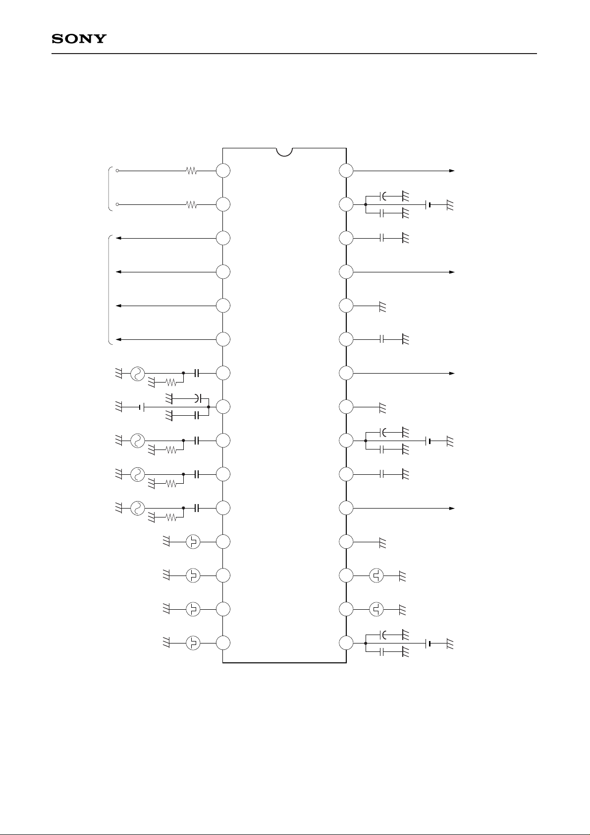
—13—
CXA2067AS
Electrical Characteristics Measurement Circuit
SYNC SEP/VDET Output
47µF
0.1µF
47µF
0.1µF
0.1µF
0.1µF
0.1µF
0.1µF
0.1µF
1
2
3
4
5
6
7
8
9
10
11
12
13
14
15
SDA
SCL
COF R
COF G
COF B
COF RGB
RIN
V
CC
GIN
SYNC IN
BIN
CLP
OSD-R
OSD-G
OSD-B
CSYNC/VDET
VCC R
S/H-R
ROUT
GND-R
S/H-G
GOUT
GND-G
VCC G
S/H-B
BOUT
GND-B
BLKING
YS
VCC B
12V
47µF
0.1µF
12V
47µF
0.1µF
12V
220
220
75
I C BUS
DAC Output
75
0.1µF
75
0.1µF
75
5V
Rch Output
Gch Output
Bch Output
17
18
19
20
21
22
23
24
25
26
27
28
29
30
16
2
Page 14

—14—
CXA2067AS
Electrical Characteristics Measurement Circuit (Frequency response)
SYNC SEP/VDET Output
47µF
0.1µF
47µF
0.1µF
0.1µF
0.1µF
0.1µF
1
2
3
4
5
6
7
8
9
10
11
12
13
14
15
SDA
SCL
COF R
COF G
COF B
COF RGB
RIN
V
CC
GIN
SYNC IN
BIN
CLP
OSD-R
OSD-G
OSD-B
CSYNC/VDET
VCC R
S/H-R
ROUT
GND-R
S/H-G
GOUT
GND-G
VCC G
S/H-B
BOUT
GND-B
BLKING
YS
VCC B
12V
47µF
0.1µF
12V
47µF
0.1µF
12V
220
220
75
I C BUS
DAC Output
75
0.1µF
0.1µF
5V
Rch Output
Gch Output
Bch Output
2
0.1µF
0.1µF
17
18
19
20
21
22
23
24
25
26
27
28
29
30
16
Page 15

—15—
CXA2067AS
The VBLK signal is extracted form the composite BLK signal input to Pin 18. The DAC data rewrite for each control is simultaneously performed,
synchronizing to the VBLK signal. The received I
2
C bus data is held by the latch till the next VBLK signal comes. Therefore, the timing of I
2
C bus data
transmission from the microcomputer is free. The V blanking pulse width input to Pin 18 should be 300µs or more.
VBLK
Bus data
transmission
DAC refresh
Enable signal
DAC refresh
signal
Transmission interval
Data 1 Data 2 Data 3
enable
disable
The latest data which was sent
before VBLK is written to DAC.
In this case, Data 1 is written.
DAC rewrite is not performed when the bus data
transmission is in progress for the VBLK interval.
The sent data is hold.
Rewrite to Data 3.
When Data 3 is not transmitted,
rewrite to Data 2.
VBLK Sync DAC Refresh System
Page 16

—16—
CXA2067AS
Application Circuit
SYNC SEP/VDET Output
47µF
0.1µF
47µF
0.1µF
0.1µF
0.1µF
0.1µF
0.1µF
0.1µF
1
2
3
4
5
6
7
8
9
10
11
12
13
14
15
SDA
SCL
COF R
COF G
COF B
COF RGB
RIN
V
CC
GIN
SYNC IN
BIN
CLP
OSD-R
OSD-G
OSD-B
CSYNC/VDET
VCC R
S/H-R
ROUT
GND-R
S/H-G
GOUT
GND-G
VCC G
S/H-B
BOUT
GND-B
BLKING
YS
VCC B
12V
47µF
0.1µF
12V
47µF
0.1µF
12V
220
220
I C BUS
DAC Output
0.1µF
0.1µF
5V
Rch Output
Gch Output
Bch Output
17
18
19
20
21
22
23
24
25
26
27
28
29
30
16
2
YS input
Application circuits shown are typical examples illustrating the operation of the devices. Sony cannot assume responsibility for
any problems arising out of the use of these circuits or for any infringement of third party patent and other right due to same.
Page 17

—17—
CXA2067AS
Notes on Operation
1. The ROUT, GOUT and BOUT outputs should be received in the high impedance state.
2. The wiring from ROUT, GOUT and BOUT to the power amplifier should be as short as possible.
3. For the decoupling capacitors for VCC and VCC R/G/B, the ceramic capacitor and the electrolysis capacitor
should be connected in parallel as closely to the IC as possible.
4. The clamp capacitors for RIN, GIN, BIN, S/H R, S/H G and S/H B should be connected as close to the IC
as possible.
5. The signals to RIN, GIN and BIN should be input via a clamp capacitor with the low impedance.
6. Set the output OFF when the VDET/CSYNC output is not used. (The cross talk may deteriorate)
Page 18

SONY CODE
EIAJ CODE
JEDEC CODE
30PIN SDIP (PLASTIC)
26.9 – 0.1
+ 0.4
15
16
30
1.778
10.16
8.5 – 0.1
+ 0.3
0.25 – 0.05
+ 0.1
0° to 15°
0.5 ± 0.1
0.9 ± 0.15
3.0 MIN
0.5 MIN
3.7 – 0.1
+ 0.4
SDIP-30P-01
SDIP030-P-0400
1
PACKAGE STRUCTURE
MOLDING COMPOUND
LEAD TREATMENT
LEAD MATERIAL
PACKAGE MASS
EPOXY RESIN
PLATING
COPPER ALLOY
1.8g
SOLDER/PALLADIUM
1.All mat surface type.
Two kinds of package surface:
2.All mirror surface type.
Package Outline Unit : mm
CXA2067AS
—18—
 Loading...