

Page 1

Description
The CXA2020M/S, is a bipolar IC designed as
EIAJ TV sound multiplexing decoder, provides
various functions including sound multiplexing
demodulation, broadcast mode identification
(stereo/bilingual discrimination display), mode
display, and muting.
Features
• Adjustment free of filter.
• High frequency stereo separation improved.
• An internal active filter greatly reduces the external
parts.
• Use of the countdown method for broadcast mode
identification eliminates the necessity of adjusting
the identification system (Cue oscillator).
• Output level: 520mVrms (1kHz, monaural, 100%).
• Internal filter eliminates interference from digital
facsimile signals.
• The discrimination time needed to shift from
multiplexing sound to monaural sound is reduced.
• Forced monaural mode can be set to operate only
for stereo broadcasts or for stereo/bilingual
broadcasts.
Applications
• Color TVs
• Hi-Fi VCRs
Structure
Bipolar silicon monolithic IC
Pin Configuration
Absolute Maximum Ratings (Ta = 25°C)
[ ( ) is the pin No. for the CXA2020S.]
• Supply voltage VCC 10 V
• Input signal (Pin 6) Vis 0.6 Vp-p
• Control voltage
(Pins 5, 12, 13, 14) Vic VCC V
• Operating temperature Topr –20 to +75 °C
• Storage temperature Tstg –65 to +150 °C
• Allowable power dissipation
PD (A2020M) 1000 mW
(A2020S) 900 mW
• LED drive current ILED 10 mA
Operating Supply Voltage Range 8.5 to 9.5 V
– 1 –
CXA2020M/S
E94Y28-ST
EIAJ Sound Multiplexing Decoder
Sony reserves the right to change products and specifications without prior notice. This information does not convey any license by
any implication or otherwise under any patents or other right. Application circuits shown, if any, are typical examples illustrating the
operation of the devices. Sony cannot assume responsibility for any problems arising out of the use of these circuits.
CXA2020S
22 pin SDIP (Plastic)
CXA2020M
28 pin SOP (Plastic)
2
3
4
5
6
7
8
9
10
11
12
13
14
15
16
17
18
19
20
21
22
1
GND
NC
REFL
Vcc
MO MODE
MPX IN
NC
CUBI
LEDST
LEDSU
LEDM
SUBI
SC OUT
SC IN
MC OUT
MC IN
L OUT
R OUT
M OUT
FOMO
MUTE
MODE
CXA2020S
2
3
4
5
6
7
8
9
10
11
12
13
14
15
16
17
18
19
20
21
22
1
GND
NC
REFL
Vcc
MO MODE
MPX IN
NC
CUBI
LEDST
LEDSU
LEDM
SUBI
SC OUT
SC IN
MC OUT
MC IN
L OUT
R OUT
M OUT
FOMO
MUTE
MODE
CXA2020M
NC
23
24
25
26
27
28
NC
NC
NC
NC
NC
CXA2020M CXA2020S
Page 2

– 2 –
CXA2020M/S
Block Diagram
CXA2020M
CXA2020S
GND
NC
REFL
Vcc
MO MODE
MPX IN
NC
CUBI
LEDST
LEDSUB
LEDMAIN
SUBI
SC OUT
SC IN
MC OUT
MC IN
L OUT
R OUT
M OUT
FOMO
MUTE
MODE
2
3
4
5
6
7
8
9
10
11
12
13
14
15
16
17
18
19
20
21
22
1
IBIAS
VOLTAGE
REGULATOR
BIAS
CURRENT
BUFFER
BIAS
VOLTAGE
MPX SIGNAL
IN AMP
4.5fH
TRAP
SUB
BPF
SUB
DET
CUE
BPF
AM
DEMOD
952Hz
BPF
COMP
LED
DRIVE
3.5f
H
VCO
CUE
CARRIER
952Hz
CLOCK
3.5f
H
CLOCK
IIL LOGIC & CONT
MAIN
OUT
OUTPUT AMP
& OUTPUT SW
MATRIX
SUB
MAIN
L R
TEST
MAINDEEM
SUBDEEM
FM
DEMOD
23
24
25
26
27
28
NC
NC
NC
NC
NC
NC
GND
NC
REFL
Vcc
MO MODE
MPX IN
NC
CUBI
LEDST
LEDSUB
LEDMAIN
SUBI
SC OUT
SC IN
MC OUT
MC IN
L OUT
R OUT
M OUT
FOMO
MUTE
MODE
2
3
4
5
6
7
8
9
10
11
12
13
1415
16
17
18
19
20
21
22
1
IBIAS
VOLTAGE
REGULATOR
BIAS
CURRENT
BUFFER
BIAS
VOLTAGE
MPX SIGNAL
IN AMP
4.5fH
TRAP
SUB
BPF
SUB
DET
CUE
BPF
AM
DEMOD
952Hz
BPF
COMP
LED
DRIVE
3.5f
H
VCO
CUE
CARRIER
952Hz
CLOCK
3.5f
H
CLOCK
IIL LOGIC & CONT
MAIN
OUT
OUTPUT AMP
& OUTPUT SW
MATRIX
SUB
MAIN
L R
TEST
MAINDEEM
SUBDEEM
FM
DEMOD
Page 3
– 3 –
CXA2020M/S
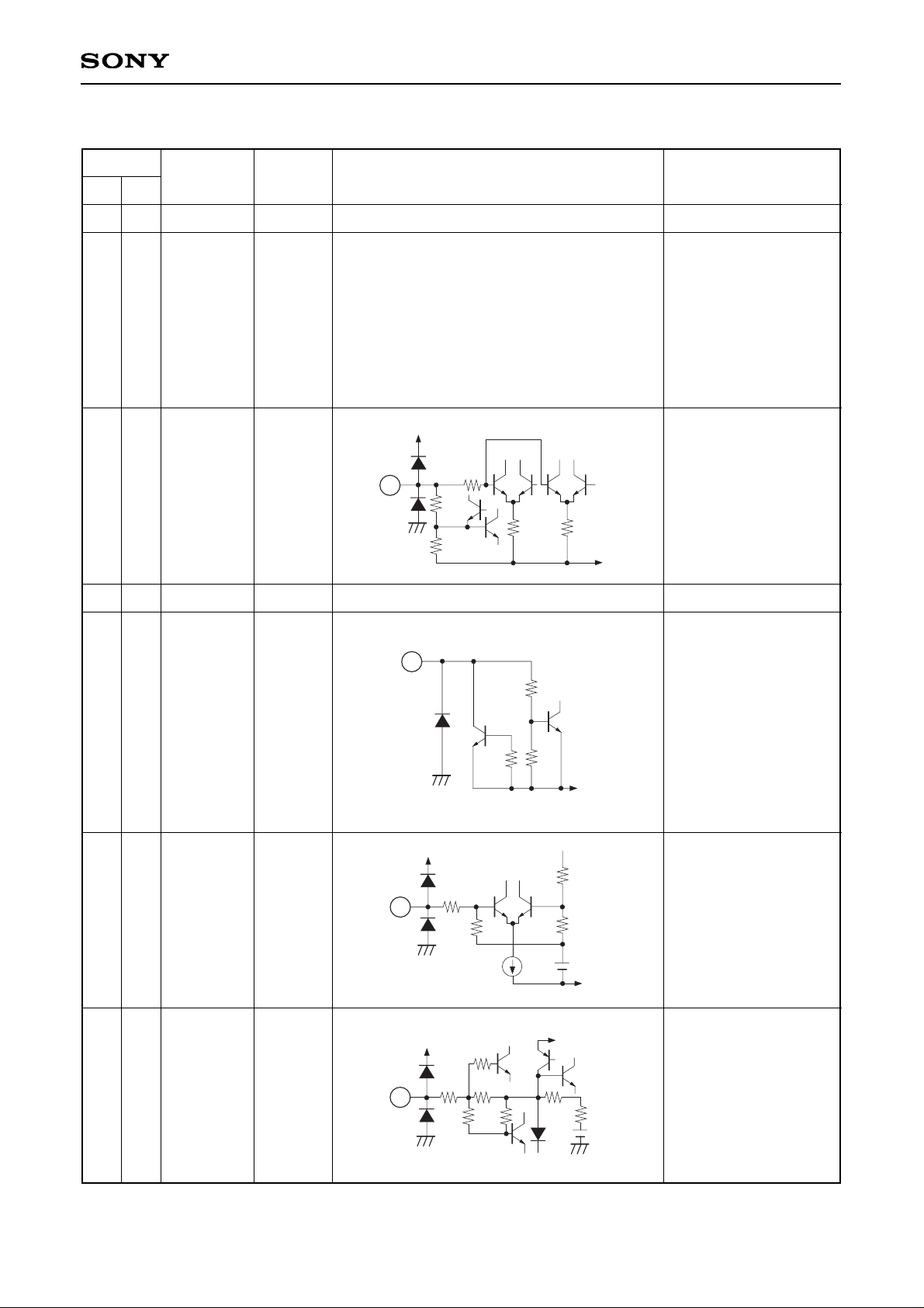
Pin Description (Ta = 25°C, VCC = 9V) The pin numbers in parentheses are for the CXA2020S.
PIn No.
SDIP
SOP
Symbol
11 GND 0 GND.
2
7
2
5
8
10
14
15
24
27
NC
—
Keep these pins open.
(They are not
connected to the chip.)
33 REFL 1.2V
The noise elimination
filter connection of
internal reference
voltage.
67 MPXIN 4.1V
Sound multiplexing
signal input.
Typical input level
= 70mVrms
(monaural, 100%)
89 CUBI 4.1V
Bias capacitor
connection of Cue
pulse generator.
56 MO MODE —
Forced monaural mode
selection.
When Low or open, the
forced monaural mode
operates for stereo
broadcasts only;
if High, the forced
monaural mode
operates for both
stereo and bilingual
broadcasts.
44 VCC — Power supply.
Pin
voltage
Equivalent circuit
Description
Vcc
147
GND
3
3.3k
20k 20k
24k
GND
(5)
10.5k
6
50k
70k
Vcc
147
80µ
GND
138k
(6)
25k
30k
4.2V
7
Vcc
147
(8)
1k
40k
40k
40k
Vcc
11k
2k
4.2V
9
—
Page 4

– 4 –
CXA2020M/S
Pin No.
SDIP
SOP
Symbol
911 LEDST
1113 LEDM
1216 MODE
1012 LEDSU
—
Mode indicator LED
connection.
Pin 11 (9): stereo
Pin 12 (10): sub
Pin 13 (11): main
—
DC voltage-based
output mode switch for
bilingual broadcasts.
1317 MUTE
—
Output muting.
When High, only DC is
output from Pins 19, 20
and 21 (15, 16 and 17).
1418 FOMO
—
Forced monaural.
When High, forced
monaural (main sound)
mode is selected and
the LED turns off.
1519 MOUT
4.1V
Main signal output.
Always outputs the main
signal component,
regardless of the
broadcast mode.
Pin
voltage
Equivalent circuit
Description
GND
(9)
(10)
(11)
11
12
13
64k
16k
10.5k
64k
16k
10.5k
64k
16k
10.5k
(12)
20k
10.5k
40k
16k
Vcc
20µ
GND
16
4.2V
GND
GND
(13)
10.5k
50k
70k
17
GND
GND
(14)
10.5k
50k
70k
18
(15)
Vcc
147
GND
17.2k
1.5m
32k
32k
Vcc
19
Page 5

– 5 –
CXA2020M/S
Pin No.
SDIP
SOP
Symbol
1620 ROUT 4.1V R-ch output.
1721 LOUT 4.1V
L-ch output.
During "TEST", the Cue
signal component
passed through the Cue
BPF is output.
1822 MCIN 4.1V
1923 MCOUT 3.4V
DC cut capacitor
connection of main
signal.
2025 SCIN 4.1V
2126 SCOUT 3.9V
DC cut capacitor
connection of sub
signal.
22
28 SUBI 4.1V
Bias capacitor
connection of sub FM
detector. "TEST" mode,
used for filter
adjustment, is
activated by grounding
this pin.
Pin
voltage
Equivalent circuit
Description
(22)
147
8k
64k
8k
Vcc
20µ80µ
16k
1.7V
4.2V
147
1k16k
Vcc
28
4.2V
147
80µ
20P
Vcc
80µ
GND
(21)
Vcc
147
147
26
(20)
Vcc
16k
25
4.2V
320µ
8k
40k
(19)
(18)
Vcc Vcc
147
147
16k
4.2V
147
160µ
147
80µ
80µ
20P
GND
Vcc
23
22
(17)
Vcc
147
GND
17.2k
1.5m
32k
32k
Vcc
21
(16)
Vcc
147
GND
17.2k
1.5m
32k
32k
Vcc
20
Page 6

– 6 –
CXA2020M/S
Electrical Characteristics Measurement Circuit (CXA2020M)
CXA2020M
GND
SIGNAL
SIG
ATT
SW5
E1
9V
C2
47µF
C1
10µF
A
GND
C3
10µF
E5
C4
10µF
R2
910
STEREO
R3
910
SUB
R4
910
MAIN
GND
E4
GND
E3
GND
E2
SW1
SW2
SW3
15kHz
LPF
CCIR
FILTER
MEASUREMENT
SYSTEM
RMS
DISTORTION
DCVOLT
L OUT
R OUT
MAIN OUT
C10
1µF
C9
1µF
C10
10µF
ON
OFF
SW6
TEST
(ON)
NORM
(OFF)
SW4
∗
ATT is set to bring L → R stereo separation to a minimum.
15
16
17
18
19
20
21
22
23
24
25
26
27
28
2
3
4
5
6
7
8
9
10
11
12
13
14
1
Page 7
– 7 –
CXA2020M/S
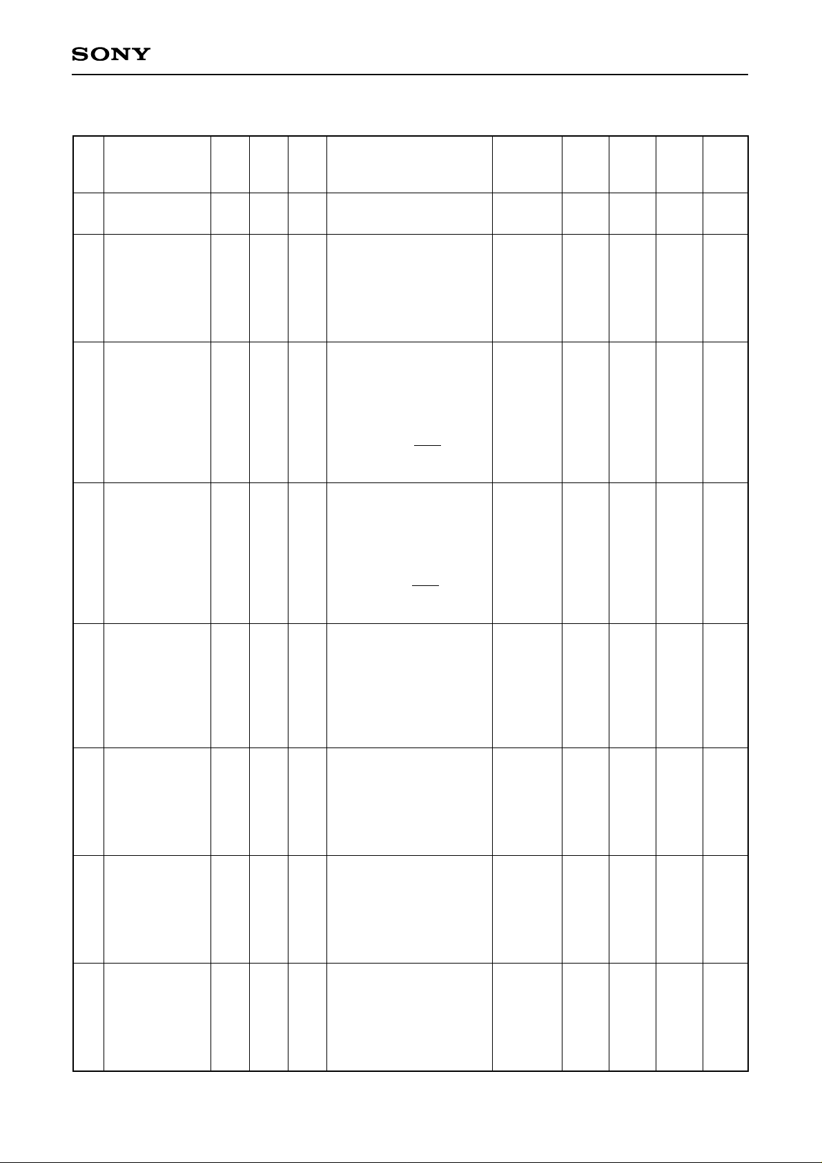
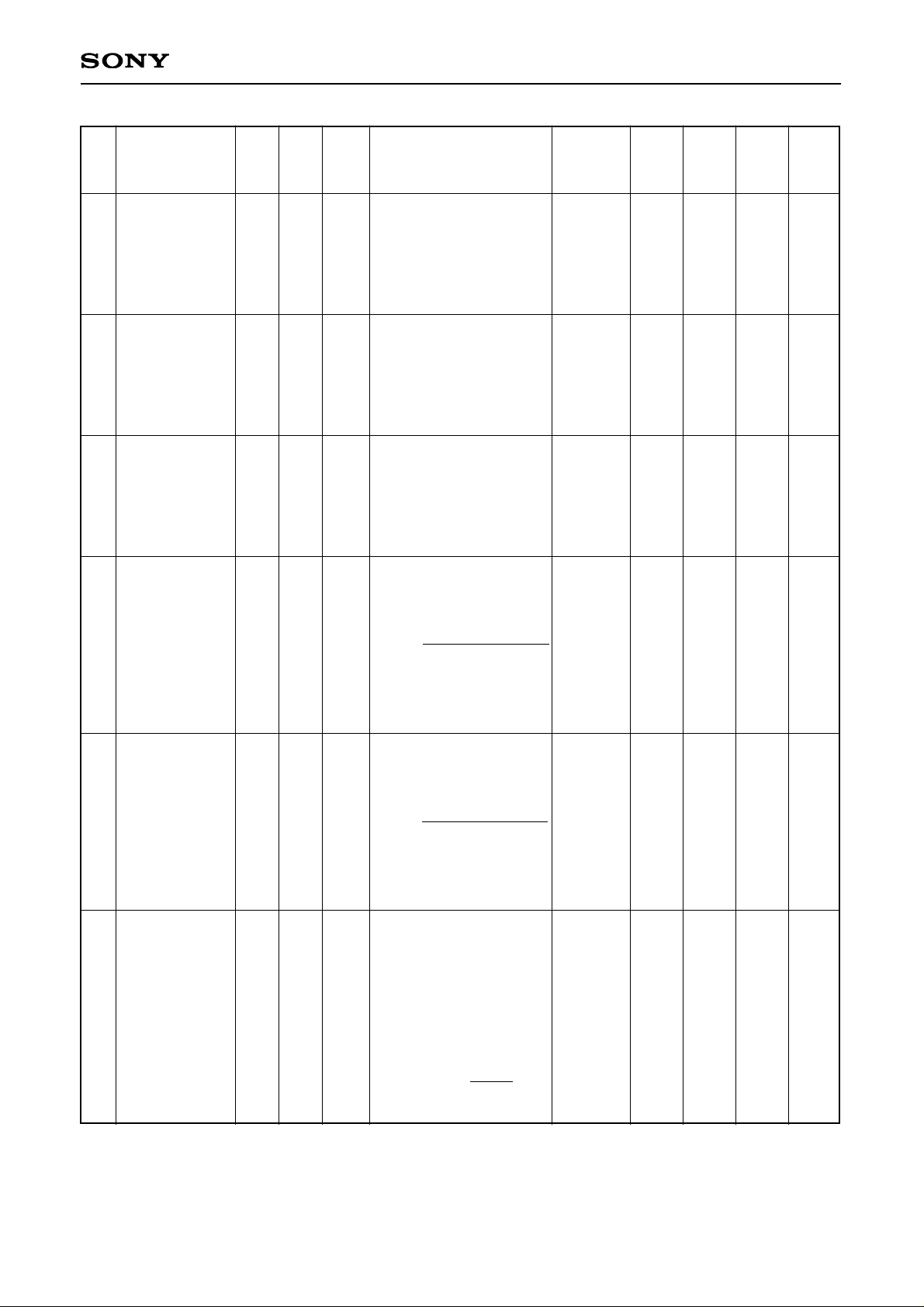
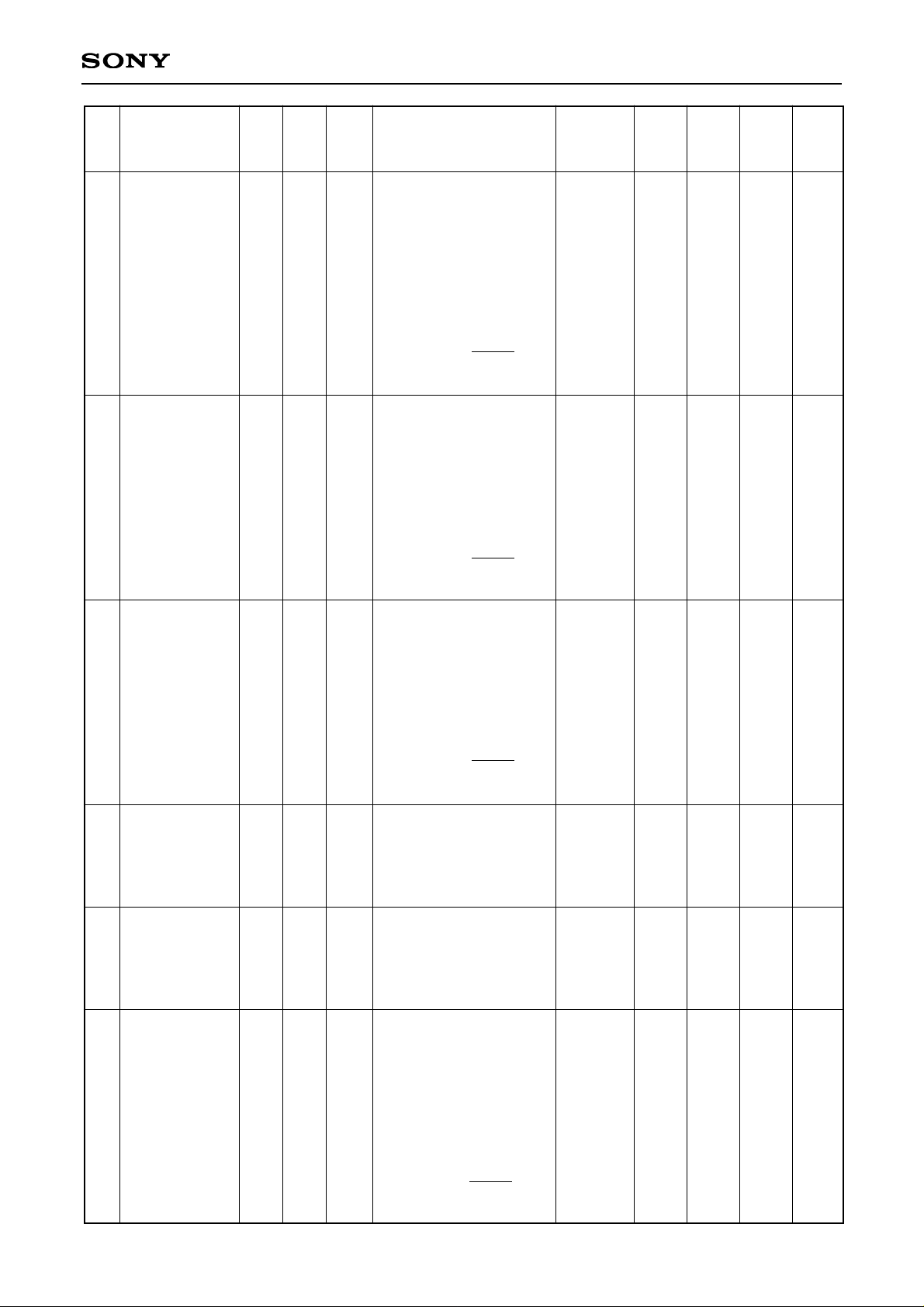
Electrical Characteristics (Ta = 25°C, VCC = 9V) The pin numbers in parentheses are for the CXA2020S.
No. Item
Symbol
SW
condi-
tions
Bias
condi-
tions
Conditions
Measure-
ment
point
Min. Typ. Max. Unit
1
2
3
4
5
6
7
8
Current
consumption
Sub output
level 400Hz
Sub frequency
characteristics
1kHz
Sub frequency
characteristics
10kHz
Sub distortion
Sub S/N ratio
Stereo
distortion
L-ch
Stereo
distortion
R-ch
ICC
Vs1
Fs1
Fs2
Ds
Ns
Dstl
Dstr
1
4
4
4
4
4
4
4
1
2
and
3
2
and
3
2
and
3
2
and
3
2
and
3
2
2
Measure current
input to Pin 4
Input signal: SIG1
Measure output amplitude
(400Hz, sine wave)
of Pins 20 and 21
(16 and 17): Vs1
(15kLPF)
Input signal: SIG2
Measure output amplitude
(1kHz, sine wave)
of Pins 20 and 21
(16 and 17): Vs2
Fs1 = 20log
(15kLPF)
Input signal: SIG3
Measure output amplitude
(10kHz, sine wave)
of Pins 20 and 21
(16 and 17): Vs3
Fs2 = 20log
(15kLPF)
Input signal: SIG2
Measure distortion
of output signal
(1kHz, sine wave)
of Pins 20 and 21
(16 and 17)
(15kLPF)
Input signal: SIG2
Measure S/N ratio
of output (1kHz)
of Pins 20 and 21
(16 and 17)
(15kLPF, RMS)
Input signal: SIG4
Measure distortion
of output signal
(1kHz, sine wave)
of Pin 21 (17)
(15kLPF)
Input signal: SIG5
Measure distortion
of output signal
(1kHz, sine wave)
of Pin 20 (16)
(15kLPF)
Pin 4
Pins 20
and 21
(16 and
17)
∗1
Pins 20
and 21
(16 and
17)
∗1
Pins 20
and 21
(16 and
17)
∗1
Pins 20
and 21
(16 and
17)
∗1
Pins 20
and 21
(16 and
17)
∗1
Pin 21
(17)
Pin 20
(16)
17
480
–1.6
–19.0
—
59
—
—
25
580
–0.6
–16.5
1
64
0.2
0.2
36
690
0
–14.0
2
—
1.5
1.5
mA
mVrms
dB
dB
%
dB
%
%
Vs2
Vs1
Vs3
Vs1
∗1
When bias condition is "3", measurement point is Pin 20 only.
Page 8

– 8 –
CXA2020M/S
9
10
11
12
13
14
15
Stereo
output level
L-ch 1kHz
Stereo
output level
R-ch 1kHz
Main
output level
MAIN OUT
Main
output level
Main
frequency
characteristics
1kHz
Main
frequency
characteristics
10kHz
Main distortion
MAIN OUT
Vstl
Vstr
Vm1
Vm2
Fm1
Fm2
Dm1
4
4
4
4
4
4
4
2
2
2
2
2
2
2
Input signal: SIG4
Measure output
amplitude
(1kHz, sine wave)
of Pin 21 (17)
(15kLPF)
Input signal: SIG5
Measure output
amplitude
(1kHz, sine wave)
of Pin 20 (16)
(15kLPF)
Input signal: SIG6
Measure output signal
(400Hz, sine wave) of
Pin 19 (15)
(15kLPF)
Input signal: SIG6
Measure amplitude of
output signal
(400Hz, sine wave) of
Pins 20 and 21 (16 and 17)
(15kLPF)
Input signal: SIG7
Measure output amplitude
(1kHz, sine wave) of
Pins 20 and 21
(16 and 17): Vm3
Fm1 = 20log
(15kLPF)
Input signal: SIG8
Measure output amplitude
(10kHz, sine wave) of
Pins 20 and 21
(16 and 17): Vm4
Fm2 = 20log
(15kLPF)
Input signal: SIG7
Measure distortion of
output signal
(1kHz, sine wave) of
Pin 19 (15)
(15kLPF)
Pin 21
(17)
Pin 20
(16)
Pin 19
(15)
Pins
20 and 21
(16 and
17)
Pins
20 and 21
(16 and
17)
Pins
20 and 21
(16 and
17)
Pin 19
(15)
440
440
480
480
–1.6
–16.0
—
540
540
580
580
–0.6
–14.0
0.2
640
640
690
690
0
–12.0
1
mVrms
mVrms
mVrms
mVrms
dB
dB
%
Vm3
Vm2
Vm4
Vm2
No. Item
Symbol
SW
condi-
tions
Bias
condi-
tions
Conditions
Measure-
ment
point
Min. Typ. Max. Unit
Page 9
– 9 –
CXA2020M/S
16
17
18
19
20
21
Main distortion
Main distortion
at maximum
input
Main S/N ratio
Stereo
separation
L → R
Stereo
separation
R → L
Cross talk
MAIN → SUB
Dm2
Dm3
Nm
Sstr
Sstl
Cms1
4
4
4
4
4
2
2
2
2
2
2
2
Input signal: SIG7
Measure distortion of
output signal
(1kHz, sine wave) of
Pins 20 and 21
(16 and 17) (15kLPF)
Input signal: SIG9
Measure distortion of
output signal
(1kHz, sine wave) of
Pins 20 and 21
(16 and 17) (15kLPF)
Input signal: SIG7
Measure S/N ratio of
output signal (1kHz) of
Pins 20 and 21
(16 and 17)
(15kLPF. RMS)
Input signal: SIG4
Sstr =
20log
(dB)
(15kLPF)
Input signal: SIG5
Sstl =
20log
(dB)
(15kLPF)
Input signal: SIG15
Calculate the level
difference between the
output amplitude of Pins
20 and 21 (16 and 17)
(Vms1) and the
measured value (Vm3)
in measurement No. 13
Cms1 = 20log (dB)
(15kLPF, 1kBPF)
Pins
20 and 21
(16 and
17)
Pins
20 and 21
(16 and
17)
Pins
20 and 21
(16 and
17)
Pins
20 and 21
(16 and
17)
Pins
20 and 21
(16 and
17)
Pins
20 and 21
(16 and
17)
—
—
65
35
35
55
0.2
0.3
73
45
45
58
1
2
—
—
—
—
%
%
dB
dB
dB
dB
Output amplitude
Pin 21 (17)
Output amplitude
Pin 20 (16)
Output amplitude
Pin 20 (16)
Output amplitude
Pin 21 (17)
Vm3
Vms1
No. Item
Symbol
SW
condi-
tions
Bias
condi-
tions
Conditions
Measure-
ment
point
Min. Typ. Max. Unit
Page 10
– 10 –
CXA2020M/S
22
23
24
25
26
27
Cross talk
SUB → MAIN
Cross talk
MAIN → SUB
BOTH mode
Cross talk
SUB → MAIN
BOTH mode
Residual
carrier
SUB
Residual
carrier
MAIN
Mute volume
MAIN
Csm1
Cms2
Csm2
Lcs
Lcm
Mm
2
2
2
3
3
4
1
3
3
2
1
4
Input signal: SIG2
Calculate the level
difference between the
output amplitude of Pins
20 and 21 (16 and 17)
(Vsm1) and the
measured value (Vs2)
in measurement No. 3.
Csm1 = 20log (dB)
(15kLPF, 1kBPF)
Input signal: SIG15
Calculate the level
difference between the
output amplitude of
Pin 20 (16) (Vms2) and
the output amplitude of
Pin 21 (17) (Vms3).
Cms2 = 20log (dB)
(15kLPF, 1kBPF)
Input signal: SIG2
Calculate the level
difference between the
output amplitude of
Pin 21 (17) (Vsm2) and
the output amplitude of
Pin 20 (16) (Vsm3).
Csm2 = 20log (dB)
(15kLPF, 1kBPF)
Input signal: SIG11
Measure subcarrier
component amplitude
of the output of Pins 20
and 21 (16 and 17).
Input signal: SIG11
Measure the subcarrier
component amplitude
of the output of Pins 20
and 21 (16 and 17).
Input signal: SIG7
Calculate the level
difference between the
output amplitude of Pins
20 and 21 (16 and 17)
(VMm) and the
measured value (Vm3)
in measurement No. 13.
Mm = 20log (dB)
(15kLPF, 1kBPF)
Pins
20 and 21
(16 and
17)
Pins
20 and 21
(16 and
17)
Pins
20 and 21
(16 and
17)
Pins
20 and 21
(16 and
17)
Pins
20 and 21
(16 and
17)
Pins
20 and 21
(16 and
17)
60
55
60
—
—
70
70
58
70
10
12
80
—
—
—
30
20
—
dB
dB
dB
mVrms
mVrms
dB
Vs2
Vsm1
Vms3
Vms2
Vsm3
Vsm2
Vm3
VMm
No. Item
Symbol
SW
condi-
tions
Bias
condi-
tions
Conditions
Measure-
ment
point
Min. Typ. Max. Unit
Page 11

– 11 –
CXA2020M/S
28
29
30
31
32
33
34
Mute volume
SUB
Mute volume
stereo
DC offset
stereo L-ch
DC offset
stereo R-ch
DC offset
MAIN OUT
Cue detection
sensitivity
SUB detection
sensitivity
Ms
Mst
Ostl
Ostr
Om
CD
SD
4
4
3
3
3
4
4
4
2
and
4
2
and
4
2
and
4
2
and
4
2
2
Input signal: SIG2
Caluculate the level
difference between the
output amplitude of Pins
20 and 21 (16 and 17)
(VMs) and the
measured value (Vs2)
in measurement No. 3.
Ms = 20log (dB)
(15kLPF, 1kBPF)
Input signals: SIG4, 5
Measure the level
difference between the
output signals of Pins 20
and 21 (16 and 17)
under bias conditions
2 and 4.
Mst =
20log
Input signal: SIG18
Measure the fluctuation
in the output DC level of
Pin 21 (17) under bias
conditions 2 and 4.
Input signal: SIG18
Measure the fluctuation
in the output DC level of
Pin 20 (16) under bias
conditions 2 and 4.
Input signal: No signal
Measure the fluctuation
in the output DC level of
Pin 19 (15) under bias
conditions 2 and 4.
Input signal: SIG12
Change SIG12 and
measure amount of
attenuation at the point
"monaural" switches to
"Sound multiplex".
Input signal: SIG13
Change SIG13 and
measure amount of
attenuation at the point
"monaural" switches to
"Sound multiplex".
Pins
20 and 21
(16 and
17)
Pins
20 and 21
(16 and
17)
∗2
Pin 21
(17)
Pin 20
(16)
Pin 19
(15)
—
—
70
70
—
—
—
9
10
80
80
20
20
20
14
13
—
—
100
100
100
17
18
dB
dB
mV
mV
mV
dB
dB
Vs2
VMs
Measured value
under bias
condition 2 (mVrms)
Measured value
under bias
condition 4 (mVrms)
∗2
Measure Pin 21 for SIG4 input; Pin 20 for SIG5 input.
No. Item
Symbol
SW
condi-
tions
Bias
condi-
tions
Conditions
Measure-
ment
point
Min. Typ. Max. Unit
Page 12

– 12 –
CXA2020M/S
35
36
Cue BPF gain
4.5fH trap
attenuation
level
CGTG5
6
2
2
Input signal: SIG14
Measure the output
amplitude of Pin 21 (17).
Input signal: SIG16, 17
Measure output
amplitude of Pin 28 (22)
and then measure the
level difference in the
output signal for SIG16
input and SIG17 input.
TG =
20log
Pin 21
(17)
Pin 28
(22)
3302048038620—mVrms
dB
Measured value
for SIG16
(mVrms)
Measured value
for SIG17
(mVrms)
SW Condition Table
1 2 3 4 5 6
SW
NO
1
2
3
4
5
6
off
off
off
on
off
off
BIAS Condition Table
E5
BIAS
NO
1
2
3
4
0.5V
0.5V
0.5V
0.5V
E4
0.5V
0.5V
0.5V
0.5V
E2
0.5V
4.5V
2.5V
4.5V
E1
9V
9V
9V
9V
E3
0.5V
0.5V
0.5V
4.5V
off
on
off
off
off
off
off
off
on
off
on
on
off
off
off
off
on
off
off
off
off
off
on
on
off
off
off
off
off
on
No. Item
Symbol
SW
condi-
tions
Bias
condi-
tions
Conditions
Measure-
ment
point
Min. Typ. Max. Unit
Page 13

– 13 –
CXA2020M/S
Input Signal Definition
SIG1 : Sound MPX signal
Main :0%
Sub :400Hz, 100% MOD
Cue : Bilingual
SIG2 : Sound MPX signal
Main :0%
Sub :1kHz, 100% MOD
Cue : Bilingual
SIG3 : Sound MPX signal
Main :0%
Sub :10kHz, 100% MOD
Cue : Bilingual
SIG4 : Sound MPX signal
L-ch :1kHz, 100%
R-ch : 0%
Cue : Stereo
SIG5 : Sound MPX signal
L-ch :0%
R-ch : 1kHz, 100%
Cue : Stereo
SIG6 : Sound MPX signal
Main :400Hz, 100%
Sub :Carrier off
Cue : Cue signal off
SIG7 : Sound MPX signal
Main :1kHz, 100%
Sub :Carrier off
Cue : Cue signal off
SIG8 : Sound MPX signal
Main :10kHz, 100%
Sub :Carrier off
Cue : Cue signal off
SIG9 : Sound MPX signal
Main :1kHz, 300%
Sub :Carrier off
Cue : Cue signal off
SIG10 : Sound MPX signal
L-ch : 1kHz, 100%
R-ch : 0%
Cue : Cue signal off
SIG11 : Sound MPX signal
Main : 0%
Sub : 0% (Carrier only)
Cue : Bilingual
SIG12 : Sound MPX signal
Main : 0%
Sub : 0% (Carrier only)
Cue : Bilingual (level adjusted to minimum)
SIG13 : Sound MPX signal
Main : 0%
Sub : 0% (level adjusted to minimum)
Cue : Bilingual
SIG14 : 55.069kHz sine wave
5.6mVrms
SIG15 : Sound MPX signal
Main : 1kHz, 100%
Sub : 0% (Carrier only)
Cue : Bilingual
SIG16 : 31.47kHz sine wave
42mVrms
SIG17 : 70.80kHz sine wave
42mVrms
SIG18 : Sound MPX signal
L-ch : 0%
R-ch : 0%
Cue : Stereo
∗
Sound MPX signal level is defined as 100% MONO
at 1Vp-p.
Page 14

– 14 –
CXA2020M/S
Output and LED On/Off Table
MODE SW
SUB BOTH MAIN
Forced
monaural
MODE
Forced
monaural
MUTE
L R MAIN
STEREO
SUB MAIN
Output condition
LED On/Off condition
Broadcast
condition
Stereo
×
×
×
ON
ON
×
×
×
×
×
×
×
ON
ON
×
×
×
×
×
×
×
ON
ON
×
×
×
×
×
×
×
F.MONO
F.MONO
F.MONO
F.MAIN
F.MAIN
F.MAIN
F.MAIN
×
×
×
OFF
ON
×
×
×
×
OFF
OFF
OFF
ON
×
×
×
OFF
OFF
ON
OFF
OFF
OFF
OFF
OFF
OFF
OFF
ON
OFF
ON
L
L + R
DC
SUB
MAIN
MAIN
SUB
MAIN
MAIN
MAIN
DC
MONO
DC
R
L + R
DC
SUB
SUB
MAIN
SUB
SUB
MAIN
MAIN
DC
MONO
DC
L + R
L + R
DC
MAIN
MAIN
MAIN
MAIN
MAIN
MAIN
MAIN
DC
MONO
DC
ON
OFF
OFF
OFF
OFF
OFF
OFF
OFF
OFF
OFF
OFF
OFF
OFF
OFF
OFF
OFF
ON
ON
OFF
ON
ON
OFF
OFF
OFF
OFF
OFF
OFF
OFF
OFF
OFF
ON
ON
OFF
ON
ON
OFF
OFF
OFF
OFF
Bilingual
Monaural
×: No response
Control Voltage Range The information in parentheses is for the CXA2020S.
MODE SW
Pin 16 (Pin12)
SUB
BOTH
MAIN
on
off
on
off
F.MAIN
F.MONO
Voltage range
4.5V to VCC
2V to 3V(or open)
0V to 0.5V
3V to VCC
0V to 0.5V (or open)
3V to VCC
0V to 0.5V (or open)
3V to VCC
0V to 0.5V (or open)
Forced monaural
Pin 18 (Pin 14)
MUTE
Pin 17 (Pin 13)
Forced monaural mode
Pin 6 (Pin 5)
Description of Operation The information in parentheses is for the CXA2020S.
The sound mutiplexing signal input from Pin 7 (Pin 6) is passed through IN AMP and is applied to the Cue
BPF, Sub BPF, and Main de-emphasis circuit.
1. Discrimination circuits
Cue BPF passes only the Cue signal component from the multiplex signal. In the AM demodulator, the
signal (AM wave) is AM detected and one of two sine waves is generated, either a 922.5Hz signal for
bilingual broadcasts or a 982.5Hz signal for stereo broadcasts.
In the 952Hz BPF, the 3.5fH carrier component is eliminated from the Cue signal after AM wave detection.
The Cue signal, from which the carrier component has been eliminated, is waveform shaped by COMP,
with the resulting 922.5Hz or 982.5Hz pulse being applied to the Logic section.
In the 3.5fH VCO, a 3.5fH pulse locked onto the Cue signal carrier (3.5fH) is created and sent to the Logic
section.
In the Logic section, the broadcast mode is identified using the countdown method. Depending on this
result as well as the presence of a SUB signal from SUB detector and the MUTE ON/OFF, MODE
switching, and FOMO ON/OFF instructions from CONT, the output switching control signal is created. This
signal is used to control the output condition of OUTPUT SW and MAIN OUT.
Page 15
– 15 –
CXA2020M/S
2. Main circuits
In MAIN DEEM, de-emphasis is applied to the Main signal component and the Sub and Cue components
are removed.
After passing through the MAIN DEEM, the Main signal is applied to MATRIX, OUTPUT AMP, and
MAINOUT.
3. Sub circuits
In SUB BPF, only the SUB signal component out of multiplex signals is passed through. In the 4.5fH trap,
the digital facsimile signal component is removed.
In FM Demod, the SUB signal is FM demodulated.
In SUB DEEM, the FM demodulated Sub signal is de-emphasized and the carrier component is removed.
After passing through SUB DEEM, the Sub signal is applied to MATRIX and OUTPUT AMP.
4. MATRIX and output circuits
In MATRIX, the L and R signals are created by adding and subtracting the Main signal from MAIN DEEM
and the Sub signal from SUB DEEM in stereo broadcast.
In OUTPUT AMP and OUTPUT SW, the output signal is switched under the control of Logic.
In addition, MAIN OUT always outputs the MAIN signal component, regardless of the broadcast mode.
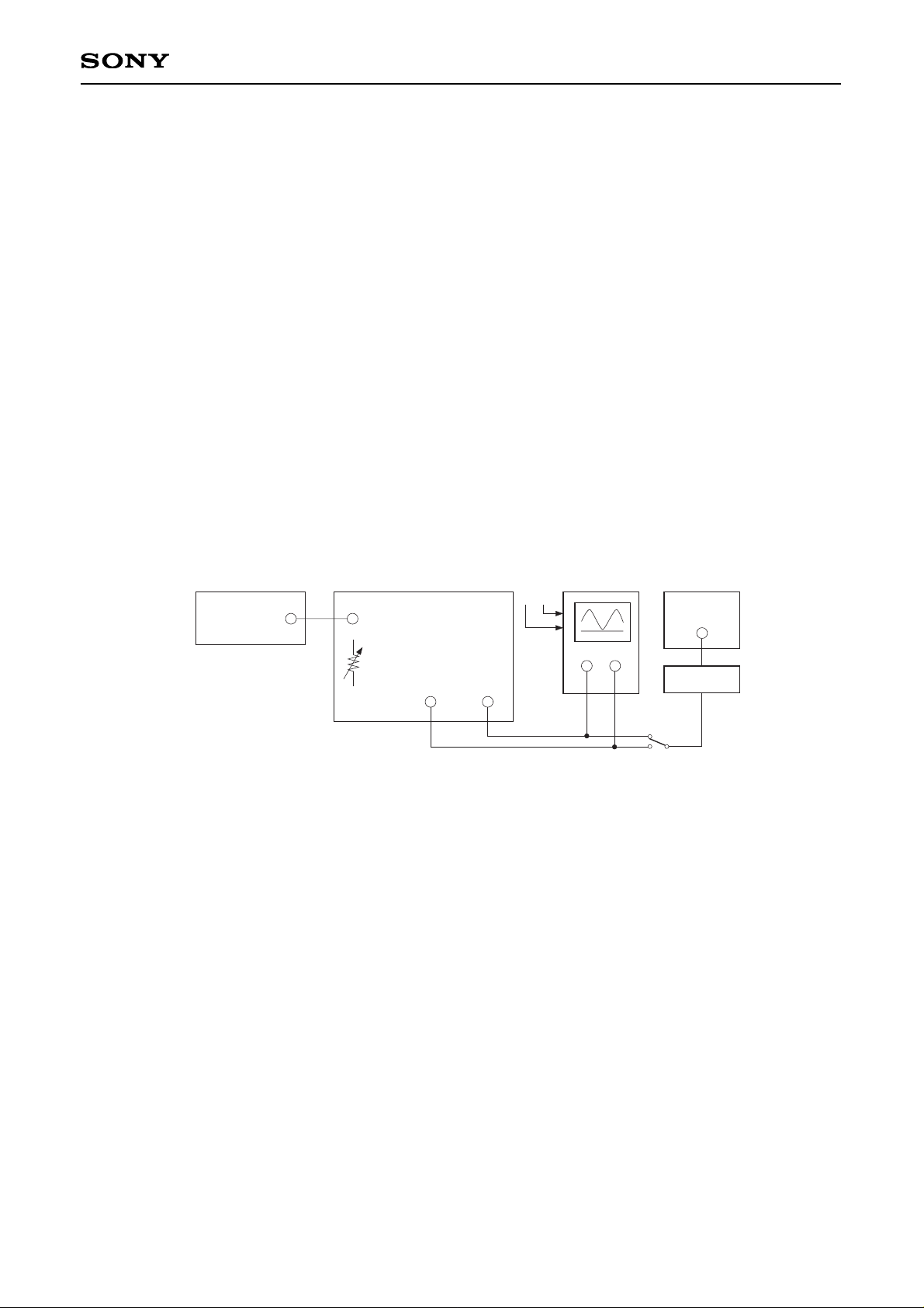
Adjustment
Separation adjustment
Fig. 1
Procedure
1) Connect components as shown in Fig. 1. (Set SW4 to NORM.)
2) Set the encoder to stereo mode, and input a 100% modulated 1kHz signal; also set the encoder so that
only the L-ch is output.
3) Monitor the oscilloscope and AC voltmeter and adjust VR2 so that the R-ch is at a minimum.
(Separation standard: 35dB or more)
EIAJ sound multiplexing encoder
MPX IN
VR2
Oscilloscope
Application circuit
L. OUT
R. OUT
LR
CH1 CH2
Switch
1kHz BPF
AC Voltmeter
Page 16
– 16 –
CXA2020M/S
CXA2020S
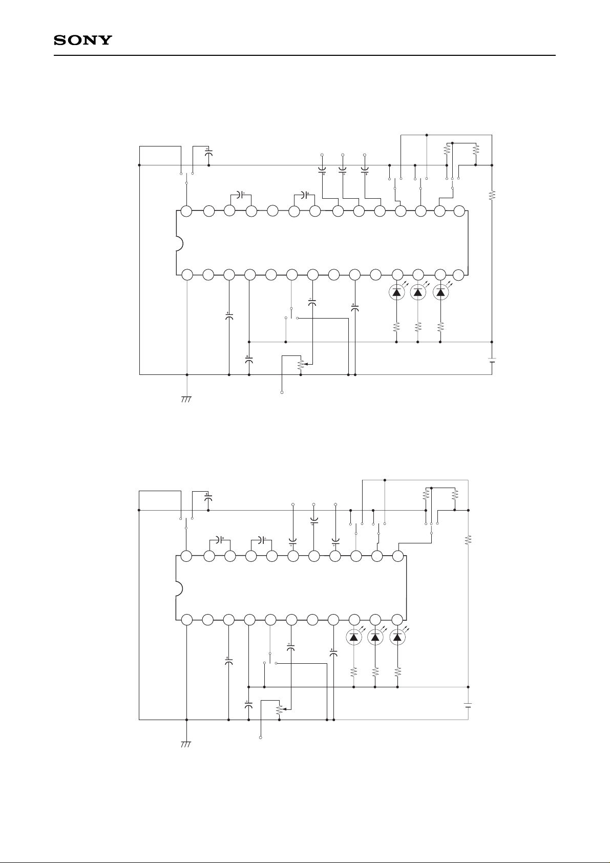
Application Circuit
CXA2020M
CXA2020M
2
3
4
5
6
7
8
9
10
11
12
13
14
15
16
17
18
19
20
21
22
1
GND
C2
47µF
C1
10µF
C3
10µF
C4
10µF
R2
910
STEREO
R3
910
SUB
R4
910
MAIN
R7
3.6k
L OUT
R OUT
MAIN OUT
C8
1µF
C9
1µF
C10
10µF
TEST
(ON)
NORM
(OFF)
SW4
VR2
1k
MPX IN
70mVrms
(MONO
100%)
SW5
∗
F. MAIN
F. MONO
Vcc
9V
SUB
MAIN
SW1
BOTH
R5
2.4k
R6
2.4k
SW2
ON
OFF
ON
SW3
OFF
C5
10µF
C7
10µFC610µF
23
24
25
26
27
28
∗
SW5:
F. MONO- Forced monaural mode operates only for stereo.
F. MAIN- Forced monaural mode operates for both stereo and bilingual.
CXA2020S
2
3
4
5
6
7
8
9
10
11
12
13
1415
16
17
18
19
20
21
22
1
GND
C2
47µF
C1
10µF
C3
10µF
C4
10µF
R2
910
STEREO
R3
910
SUB
R4
910
MAIN
R7
3.6k
L OUT
R OUT
MAIN OUT
C8
1µF
C9
1µF
C10
10µF
TEST
(ON)
NORM
(OFF)
SW4
VR2
1k
MPX IN
70mVrms
(MONO
100%)
SW5
∗
F. MAIN
F. MONO
Vcc
9V
SUB
MAIN
SW1
BOTH
R5
2.4k
R6
2.4k
SW2
ON
OFF
ON
SW3
OFF
C5
10µF
C7
10µF
C6
10µF
∗
SW5:
F. MONO- Forced monaural mode operates only for stereo.
F. MAIN- Forced monaural mode operates for both stereo and bilingual.
Application circuits shown are typical examples illustrating the operation of the devices. Sony cannot assume responsibility for
any problems arising out of the use of these circuits or for any infringement of third party patent and other right due to same.
Page 17
– 17 –
CXA2020M/S
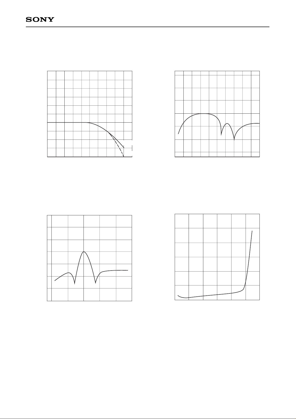
Example of Representative Characteristics
De-emphasis characteristics
Output level [dB]
Frequency [Hz]
Main
100 1k 10k
–15
–10
–5
0
SUB BPF frequency characteristics
Output level [dB]
Frequency [kHz]
10
–60
–40
–20
0
20 30 40 50 60 70 80 10090
Cue BPF frequency characteristics
Attenuation level [dB]
Frequency [Hz]
3.5f
H
–40k
–60
–40
–20
0
3.5fH
–20k
3.5fH 3.5fH
+20k
3.5fH
+40k
MAIN distortion characteristics
Distortion [%]
MAIN modulation factor [%]
100
1
2
3
200 300 400 500
Sub
Page 18
– 18 –
CXA2020M/S
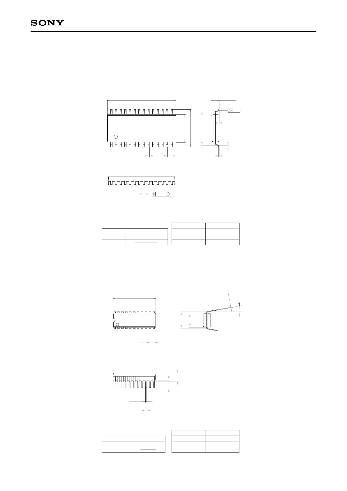
Package Outline Unit: mm
CXA2020M
CXA2020S
SONY CODE
EIAJ CODE
JEDEC CODE
SOP-28P-L04
PACKAGE STRUCTURE
PACKAGE MATERIAL
LEAD TREATMENT
LEAD MATERIAL
PACKAGE WEIGHT
42 ALLOY
SOLDER PLATING
EPOXY / PHENOL RESIN
28PIN SOP (PLASTIC) 375mil
18.8 – 0.1
+ 0.4
1528
0.45 ± 0.1
1.27
9.3
2.3 – 0.15
+ 0.4
0.1 – 0.05
+ 0.2
0.5 ± 0.2
0.2 – 0.05
+ 0.1
7.6 – 0.1
+ 0.3
10.3 ± 0.4
14
0.15
M
± 0.12
∗SOP028-P-0375-D
1
0.7g
SONY CODE
EIAJ CODE
JEDEC CODE
PACKAGE STRUCTURE
MOLDING COMPOUND
LEAD TREATMENT
LEAD MATERIAL
PACKAGE WEIGHT
EPOXY RESIN
SOLDER PLATING
COPPER ALLOY
22PIN SDIP (PLASTIC)
SDIP-22P-01
SDIP022-P-0300
0.95g
1.778
11
12
1
22
19.2 – 0.1
+ 0.4
7.62
6.4 – 0.1
+ 0.3
0.25 – 0.05
+ 0.1
0° to 15°
0.5 ± 0.1
0.9 – 0.1
+ 0.15
3.25 – 0.2
+ 0.15
0.51 MIN
3.9 – 0.1
+ 0.4
 Loading...