

Page 1

CXA2000Q
For the availability of this product, please contact the sales office.
Y/C/RGB/D for PAL/NTSC Color TVs
Description
The CXA2000Q is a bipolar IC which integrates the
luminance signal processing, chroma signal
processing, RGB signal processing, and sync and
deflection signal processing functions for NTSC/PAL
system color TVs onto a single chip. This IC includes
deflection processing functions for wide-screen TVs,
and is also equipped with a SECAM decoder
interface, making it possible to construct a TV
system that supports multiple color systems.
Features
• I2C bus compatible
• Compatible with both PAL and NTSC systems
(also compatible with SECAM if a SECAM decoder is connected)
• Built-in deflection compensation circuit capable of supporting various wide modes
• Countdown system eliminates need for H and V oscillator frequency adjustment
• Automatic identification of 50/60Hz vertical frequency (forced control possible)
• Non-interlace display support (even/odd selectable)
• Automatic identification of PAL, NTSC, and SECAM color systems (forced control possible)
• Automatic identification of 4.43MHz/3.58MHz crystal (forced control possible)
• Non-adjusting Y/C block filter
• One CV input, one set of Y/C inputs, two sets of analog RGB inputs (one set of which can serve as both
analog and digital inputs)
• Built-in AKB circuit
• Support for forcing YS1 off
64 pin QFP (Plastic)
Applications
Color TVs (4:3, 16:9)
Structure
Bipolar silicon monolithic IC
Absolute Maximum Ratings (Ta = 25°C, SGND, DGND = 0V)
• Supply voltage SVCC1, 2, DVCC1, 2 –0.3 to 12 V
• Operating temperature Topr –20 to +65 °C
• Storage temperature Tstg –65 to +150 °C
• Allowable power dissipation PD 1.7 W
(when mounted on 50mm × 50mm board)
• Voltages at each pin –0.3 to SVCC1, SVCC2,
DVCC1, DVCC2 + 0.3 V
Operating Conditions
Supply voltage SVCC1, 2 9.0 ± 0.5 V
DVCC1, 2 9.0 ±0.5 V
Sony reserves the right to change products and specifications without prior notice. This information does not convey any license by
any implication or otherwise under any patents or other right. Application circuits shown, if any, are typical examples illustrating the
operation of the devices. Sony cannot assume responsibility for any problems arising out of the use of these circuits.
– 1 –
E96103-ST
Page 2
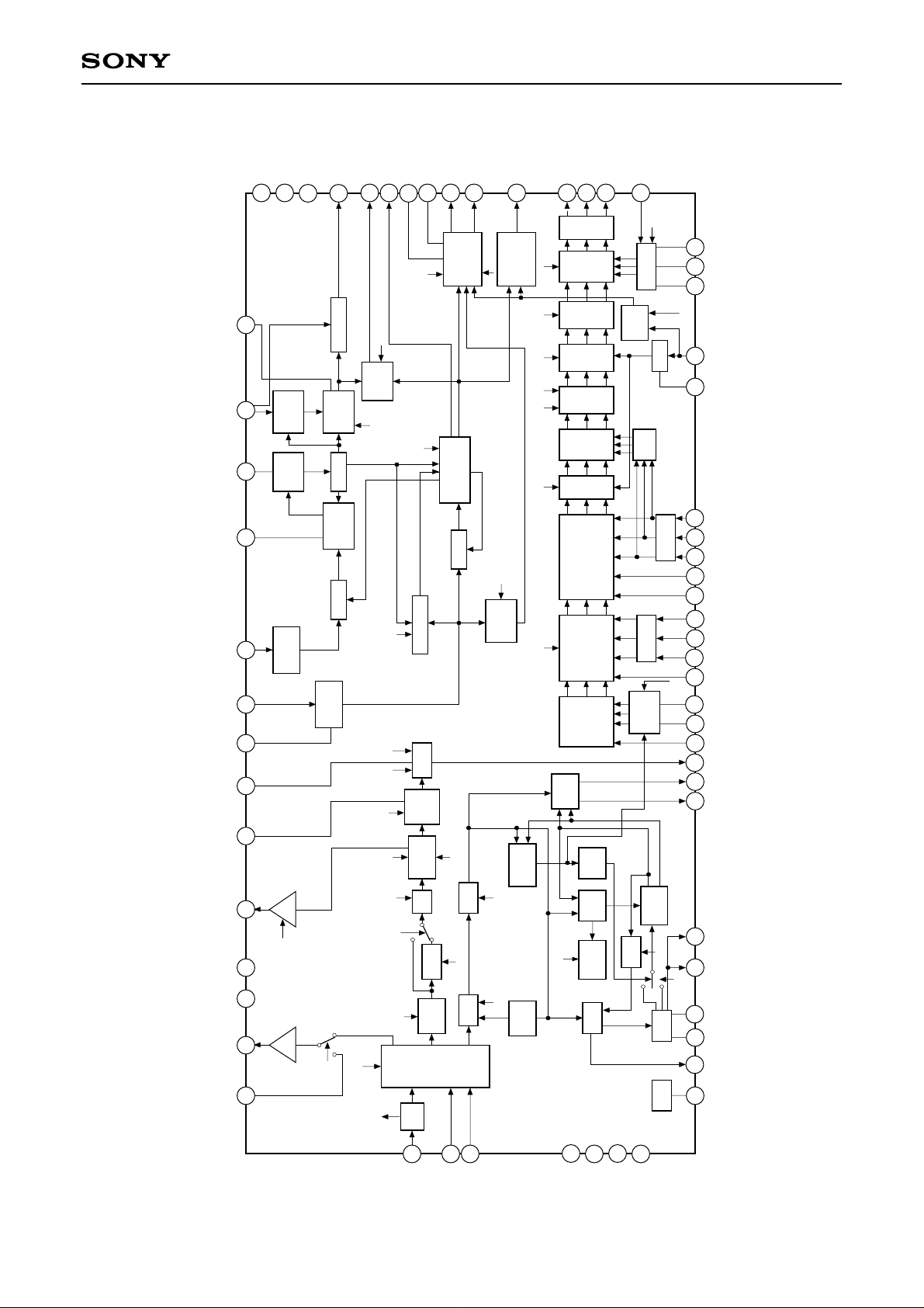
CXA2000Q
Block Diagram
CC2DVCC1
DV
44
36
L2FIL
39
HOFF
AFCPIN/
38
PHASE
CERA
41
32fH
AFCFIL
40
HSIN
47
H SYNC
VSIN
46
VSFIL
45
BLHOLD
52
DCTRAN
54
VM
49
SCL
50
51
48
56
VM OFF
2Vp-p
SDA
SYNCOUT
EXT SYNC IN
DET
VCO
SEP
6dB
DGND
42
V SYNC
EXT
HD OUT
37
H.DRIVE
SHIFT
PHASE
1/32
2fH
DET.
PHASE
GATE
SEP
CV/YC
SYNC
VAGCSH
VTIM
SCPOUT
34
10
30
VPOSI, VOFF,
SCP BGR/BGF
Sand
Castle
AFC
H POSI
C MODE
50/60 ID
V FREQ
D PICAGING
DC
DC
TRAN
SHARP
SHARP
DL
TRAP OFF
SUB CONT
S
SEP
STATUS
53
CVIN
SAWOSC
VD+OUT
32
35
WIDE
VSIZE
Count Down
D PIC
CLP
TRAN
NESS
DL
TRAP
SUB
CONT
SW
VIDEO
1Vp-p
55
YIN
VD–OUT
/VPROT
/VPROT
31
VLIN, SCORR
Gen.
Sawtooth
525/625
GATE
INTER
PRE/OVER
TOT
TRAP F0
ACC
57
CIN
E-WOUT
33
GB CUT
Gen.
WIDE
Parabola
GB DRV
BRT
γ
D-COL
PIC
INTERLACE
-LACE
YS1 OFF
1Vp-p
DET
KILLER
TOT
SUB COLOR
DET
ACC
GOUT
ROUT
24
22
BLK
OFF
CUT
GB
DRV
BRT
γ
D-
COL
MIX
OSD
PIC
SW
YS/YM
YS
SW
Y/C
MIX
DEM
ID
fsc
ID
PAL
PAL/
NTSC
COLOR SW
APC
59
20
CC1SVCC2
SV
BOUT
26
2
SGND1
IKIN
27
HV
COMP
DIG
COLOR
fsc R-Y
HUE
9
SGND2
AKB OFF
AKB
ABL
CLP
CLP
& AXIS
fsc B-Y
DEM
AXIS
HUE
VCO
IREF
25
23
21
EHT H, V
28
29
19
18
17
16
15
14
13
12
11
COL
8
7
6
5
4
3
64
XTAL
61
62 1
60
43
BSH
YM
YS2
YS1
GSH
RSH
ABLIN/
ABLFIL
B2IN
G2IN
R2IN
B1IN
G1IN
R1IN
YRET
YOUT
X443
X358
IREF
VCOMP
–(B-Y) IN
–(R-Y) IN
–(B-Y) OUT
–(R-Y) OUT
SECAMREF
FSCOUT
APCFIL
– 2 –
Page 3

Pin Configuration
CXA2000Q
BLHOLD
CVIN
DCTRAN
YIN
EXT SYNC IN
CIN
TEST
SV
CC1
APCFIL
X443
X358
NC
FSCOUT
52
53
54
55
56
57
58
59
60
61
62
63
64
51
1
SDA
50
2
SCL
VM
49
3
HSIN
SYNCOUT
48
47
5
4
46
6
VSIN
45
7
VSFIL
44
8
2
CC
DV
43
9
IREF
10
DGND
4142
11
CERA
40
12
L2FIL
AFCFIL
39
13
AFCPIN/HOFF
HDOUT
37
38
14 15
36
16
1
CC
DV
35
17
VAGCSH
SAWOSC
33
34
19
18
E-WOUT
32
30
24
23
20
VD+OUT/VPROT
VD–OUT/VPROT
31
VTIM
ABLFIL
29
ABLIN/VCOMP
28
IKIN
27
BOUT
26
BSH
25
GOUT
GSH
ROUT
22
RSH
21
SV
CC2
SGND1
SECAMREF
–(R-Y) OUT
YRET
YOUT
–(B-Y) OUT
–(B-Y) IN
–(R-Y) IN
SGND2
SCPOUT
YS1
R1IN
G1IN
B1IN
YS2
YM
R2IN
G2IN
B2IN
– 3 –
Page 4
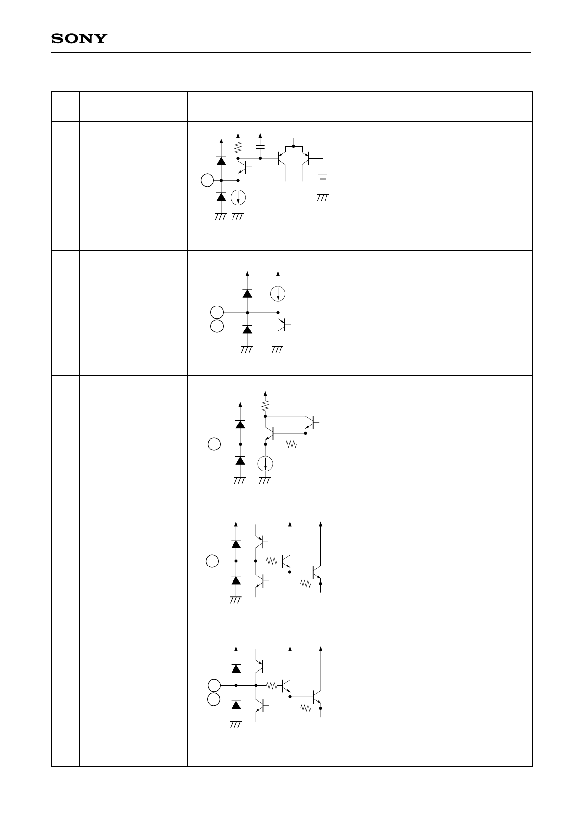
Pin Description
CXA2000Q
Pin
No.
Symbol Equivalent circuit Description
20p
6k
SECAM decoder interface. This pin
SECAMREF
1
SGND1 GND for Y/C block.
2
1
250µA
7.2V
—
serves as both a 4.43MHz output and as
a SECAM identification input/output pin.
Color difference signal outputs. Go to
3
4
–(R-Y) OUT
–(B-Y) OUT
200µA
3
4
high impedance when the SECAM
system is detected.
Standard output levels for 75% CB:
B-Y: 0.665Vp-p
R-Y: 0.525Vp-p
5
6
7
8
YOUT
YRET
–(R-Y) IN
–(B-Y) IN
500
Luminance signal output.
Black level is 3.5VDC.
5
30k
400µA
Standard output level for 100 IRE input:
1Vp-p
Luminance signal input.
6
1.5k
Clamped to 4.8V at the burst timing.
Standard input level for 100 IRE input:
1Vp-p
70k
Color difference signal inputs.
Clamped to 5.5V at the burst timing.
7
8
1.5k
70k
Standard input levels for 75% CB:
B-Y: 1.33Vp-p
R-Y: 1.05Vp-p
SGND2 GND for the RGB block.
9
– 4 –
Page 5

CXA2000Q
Pin
No.
10
11
Symbol Equivalent circuit Description
SCPOUT
YS1
11
10
40k
10k
1k
1k
100µA
Sand castle pulse output. The 0 to 5V
BGP pulse, the phase of which is
controlled through the bus, is
superimposed with the 0 to 2V H and
VBLK pulse for output.
YSSW control input.
When YS is high, the RGB1 block signal
is selected; when YS is low, the Y/C block
is selected. This function can be disabled
by the YS1OFF setting for the I2C bus.
VILMAX = 0.4V
VIHMIN = 1.0V
12
13
14
15
16
R1IN
G1IN
B1IN
YS2
YM
12
13
14
15
16
40k
40k
30k
100µA
100µA
Analog R, G and B signal inputs.
200
Input a 0.7Vp-p (no sync, 100 IRE) signal
via a capacitor.
The signal is clamped to 5.7V at the burst
timing of the signal input to the HSIN
input pin (Pin 47).
YS/YMSW YS control input.
When YS is high, the RGB2 block signal
is selected; when YS is low, the YSSW
output signal is selected.
VILMAX = 0.4V
VIHMIN = 1.0V
YS/YMSW YM control input.
When YM is high, the YSSW output
signal is attenuated by 9.6dB.
VILMAX = 0.4V
VIHMIN = 1.0V
– 5 –
Page 6

CXA2000Q
Pin
No.
17
18
19
20
21
23
25
R2IN
G2IN
B2IN
SVCC2
RSH
GSH
BSH
Symbol Equivalent circuit Description
Analog/digital (dual-purpose) RGB signal
inputs.
The input signals are input via capacitors.
100µA
200
17
18
19
30k
When using analog input, input a 0.7Vp-p
signal (no sync, 100 IRE); when using
digital input, input a signal of at least
1.5Vp-p (Vth = 1.2V).
The display level is 67 IRE. When using
digital input, digital input is selected
regardless of the YS setting.
In addition, the VM output is turned off.
These pins are clamped to 5.7V at the
burst timing of the signal input to the
sync input pin (Pin 47).
Power supply for RGB block.
200
21
23
25
Sample-and-hold for R, G and B AKB.
Connect to GND via a capacitor.
When not using AKB (manual CUTOFF
mode), R, G and B cut-off voltage can be
controlled by applying a control voltage to
each pin. The control voltage is 4.5 ± 1V.
22
24
26
27
ROUT
GOUT
BOUT
IKIN
27
22
24
26
200
1.1mA
1k
12k
50µA
R, G and B signal outputs.
2.5Vp-p is output during 100% white
input.
Input the signal converted from the CRT
beam current (cathode current Ik) to a
voltage via a capacitor. The V blanking
part is clamped to 2.7V at the V retrace
timing.
The input for this pin is the reference
pulse return, and the loop operates so
that the Rch is 1Vp-p and the G and Bch
are 0.81Vp-p. The G and Bch can be
varied by ±0.5V by the bus CUTOFF
control. When not using AKB, this pin
should be open.
– 6 –
Page 7

CXA2000Q
Pin
No.
ABLIN/VCOMP
28
ABLFIL
29
Symbol Equivalent circuit Description
ABL control signal input and VSAW high
voltage fluctuation compensation signal
input.
1.5V
High voltage compensation has linear
control characteristics for the pin voltage
range of about 8V to 1V. The control
28
147
characteristics can be varied through
EHT-V control of the bus. ABL begins to
have effect below a threshold voltage of
about 1.2V.
ABL functions as PIC/BRT-ABL (average
value type).
100k
29
1.2k
Connect a capacitor to form the LPF of
the ABL control signal.
VTIM
30
VD–OUT/VPROT
31
32
VD+OUT/VPROT
31
32
30
700
400µA
700
400µA
10k
30k
30k
1k
1k
24k
24k
V timing pulse output.
Outputs the timing pulse from V sync
identification to the end of V blanking.
Pulses are positive polarity from 1 to 6V.
During zoom mode, the V blanking pulse
which has been expanded before and
after the V sync is superimposed and
output as the 1 to 3V pulse.
V sawtooth wave output and V protect
signal input.
When a large current (3mA) is drawn
from this pin, the RGB outputs are all
blanked and "1" is output to the status
register VNG.
Serves as both a V sawtooth wave output
with the reverse polarity of VD–OUT,
and a Vprotect signal input. The Vprotect
function can even be applied to this pin.
– 7 –
Page 8

CXA2000Q
Pin
No.
33
34
Symbol Equivalent circuit Description
E-WOUT
VAGCSH
33
34
1.4k
800µA
1.2k
15k
V parabola wave output.
78k
Sample-and-hold for AGC which
maintains the V sawtooth wave at a
constant amplitude.
Connect to GND via a capacitor.
Connect a capacitor to generate the V
SAWOSC
35
36
DVCC1 Power supply for the V deflection block.
HD OUT
37
35
37
300
100
147
20k
sawtooth wave. For the capacitor, use an
MPS (metalized polyester capacitor), etc.,
with a small tan δ.
H drive signal output.
This signal is output with the open
collector.
H deflection pulse input for H AFC.
Input an about 5Vp-p pulse via a
capacitor. Set the pulse width to 10 to
12µs. This pin is also used as the hold-
38
AFCPIN/HOFF
38
147
10k
68k
down signal input for the HD output, and
if this pin is 1V or less for a 7V cycle or
4.2V
longer, the hold-down function operates
10k
and the HD output is held to 9VDC. In
addition, the RGB outputs are all blanked.
Outputs "1" to the status register XRAY.
– 8 –
Page 9

CXA2000Q
Pin
No.
39
40
L2FIL
AFCFIL
Symbol Equivalent circuit Description
Filter for H AFC.
Connect to GND via a capacitor.
The H phase can also be controlled from
39
100
this pin by leading current in and out of
this capacitor.
As the pin voltage rises, the picture shifts
to the left; as the pin voltage drops, the
picture shifts to the right.
40
1.2k
46k
CR connection for the AFC lag-lead filter.
10k
41
42
CERA
DGND
41
400µA
Connect the 32 × FH VCO ceramic
oscillator.
GND for the deflection block.
Internal reference current setting.
43
IREF
43
147
20k
Connect to GND via a resistor with an
error of less than 1% (such as a metal
film resistor).
44
DVCC2 Power supply for the H deflection block.
45
VSFIL
45
1k
– 9 –
Filter for V sync separation.
Connect to GND via a capacitor.
Page 10

CXA2000Q
Pin
No.
46
47
VSIN
HSIN
Symbol Equivalent circuit Description
15k
Sync signal input for V sync separation.
Input a 2Vp-p Y signal (or a 0.6Vp-p
sync signal).
46
147
20µA
14k
4.1V
Sync signal input for H sync separation.
47
147
10µA
3.2V
Input a 2Vp-p Y signal (or a 0.6Vp-p sync
signal).
48
49
50
SYNCOUT
VM
SCL
49
50
48
147
147
1.2k
240µA
500
1.2k
400µA
4k
40k
30k
Sync signal output for VSIN and HSIN.
The output can be selected from the
internal sync signals (Pin 53 or Pin 55) or
the external sync signal (Pin 56) by the
I2C bus.
Output signal level: 2Vp-p
(0.6Vp-p sync only)
Input/output gain: 6dB
Outputs the differential waveform of the
VM (Velocity Modulation) Y signal.
(6.6VDC, 1.1Vp-p)
The signal advanced for 200ns from
YOUT is output. The delay time versus
YIN is determined by the DL setting of
the I2C bus. This output can be turned off
through the I2C bus.
This output can also be turned off by
YS1, YM, and YS2.
I2C bus protocol SCL (Serial Clock) input.
VILMAX = 1.5V
VIHMIN = 3.5V
– 10 –
Page 11

CXA2000Q
Pin
No.
51
52
SDA
BLHOLD
Symbol Equivalent circuit Description
51
4k
I2C bus protocol SDA (Serial Data) I/O.
VILMAX = 1.5V
VIHMIN = 3.5V
VOLMAX = 0.4V
9µA
4.6V
20k
20k
1.2k
Capacitor connection for black peak hold
of the dynamic picture (black expansion).
4k
52
53
54
55
CVIN
DCTRAN
YIN
54
53
55
4k
1µA
1µA
2k
2V
4.6V
4.6V
1.2k
Composite video signal input.
Input the 1Vp-p (100% white including
sync) CV signal via a capacitor. The
sync level of the input signal is
clamped to 3.8V.
In addition, this pin detects input video
signal HSYNC, and outputs the status
via the status register CVSYNC.
Connect a capacitor that determines the
DC transmission ratio to GND.
Y signal input.
Input a 1Vp-p (100% white including
sync) Y signal via a capacitor. The
sync level of the input signal is
clamped to 3.8V.
– 11 –
Page 12

CXA2000Q
Pin
No.
56
57
Symbol Equivalent circuit Description
EXT SYNC IN
CIN
57
56
1µA
30k
50k
4.6V
External sync signal input.
Input a 0.3Vp-p sync signal (or a 1Vp-p
CV signal or Y signal) via a capacitor.
The sync level of the input signal is
clamped to 3.8V.
Chroma signal input.
Input a C signal with a burst level of
300mVp-p via a capacitor. Input signal is
5.2V
biased to 4.5V internally.
1k
Test pin.
TEST
58
59
SVCC1 Power supply for Y/C block.
60
APCFIL
58
15k
4.6V
1.2k
60
1.2k
4k
Outputs a 0 to 3V V-SYNC SEP with
positive polarity. If not used, leave this
pin open.
CR connection for the chroma APC laglead filter.
61
X443
61
Connect a 4.433619MHz crystal oscillator.
500
200µA
– 12 –
Page 13
CXA2000Q
Pin
No.
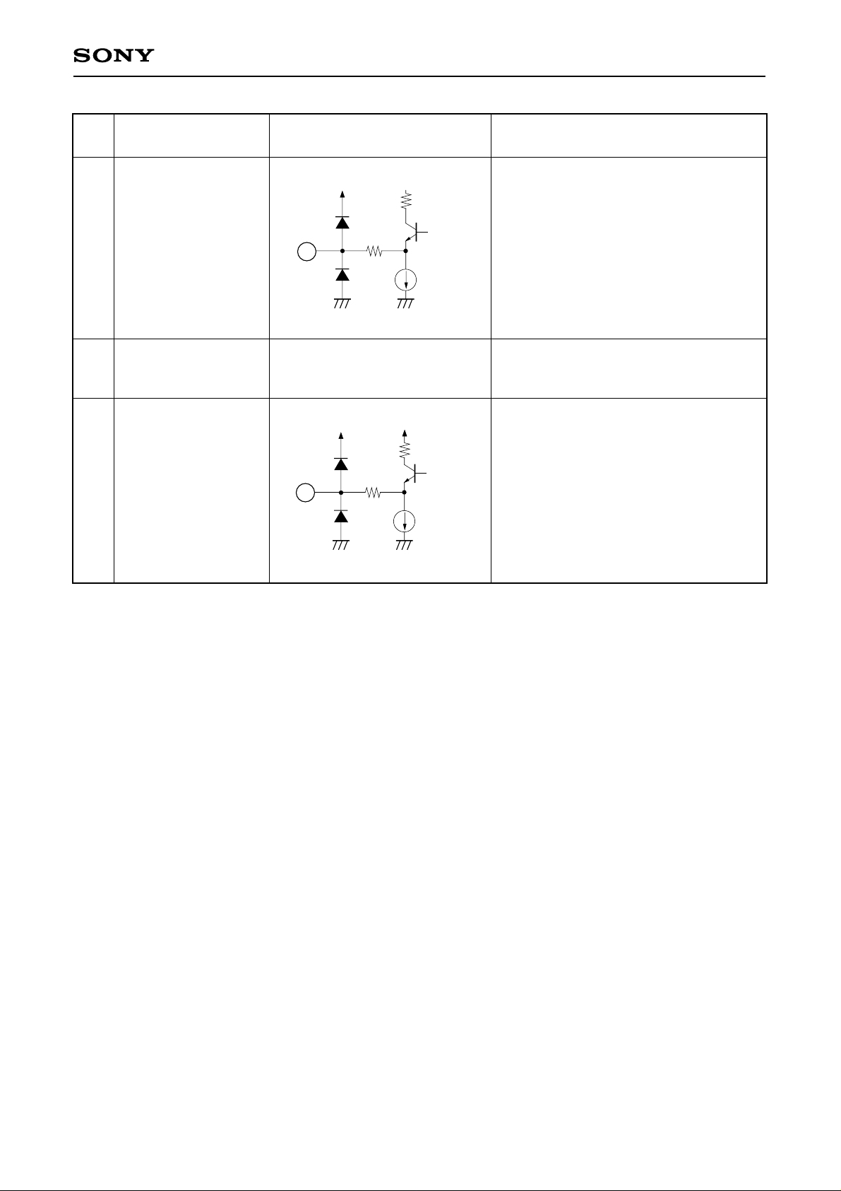
X358 Connect a 3.579545MHz crystal oscillator.
62
Symbol Equivalent circuit Description
4k
62
500
200µA
Not connected.
63
NC
Normally connected to GND to prevent
interference with other pins.
1.2k
64
FSCOUT
64
147
280µA
Subcarrier output.
Output level: 5.2VDC, 0.4Vp-p
– 13 –
Page 14

CXA2000Q
mA
86
65
mA
65
48
kHz
15.90
15.734
42
30
C Bus Register Initial Settings".
2
Measurement contents Min. Typ. Max. Unit
Measure the pin inflow current.
Measure the pin inflow current.
15.55
HDRIVE output frequency
Hz
400
—
–400
C status register
2
H is shifted from
HLOCK is 1 (the pull-in range
when f
Confirm that I
µs
26.5
25.5
24.5
15.734kHz).
Measure the pulse width for the section
where the HDRIVE output is high.
µs
12.6
12.1
11.6
VBGPh
µs
3.3
2.9
2.5
VBLKh
V
1.1
1.0
0.9
VSp-p
46: VSIN in
V
3.1
3.0
2.9
VDRIVE+
Measure the VDRIVE output Vp-p.
VSdc
10.79ms
20, 59
36, 44
37
—
Measurement pins
C bus register as shown in "I
2
Measurement conditions
CC = 9.0V,
V
CC = 9.0V,
Bus data = center
V
Bus data = center
AFC MODE = 0h
SYNCIN: composite sync
Symbol
SICC
DICC
fHFR
∆fHR
• Measures the following after setting the I
37
SYNCIN: composite sync
HDw
10
SCP
Measure the pulse width for the
VBLKh
10
section where the BLK output is high.
SCP
Measure the pulse width for the section
where the BGP output is high.
VBGPh
31, 32
VSp-p
31, 32
SYNCIN: composite sync
VSdc
Signal block current
consumption
Sync block current
consumption
1
2
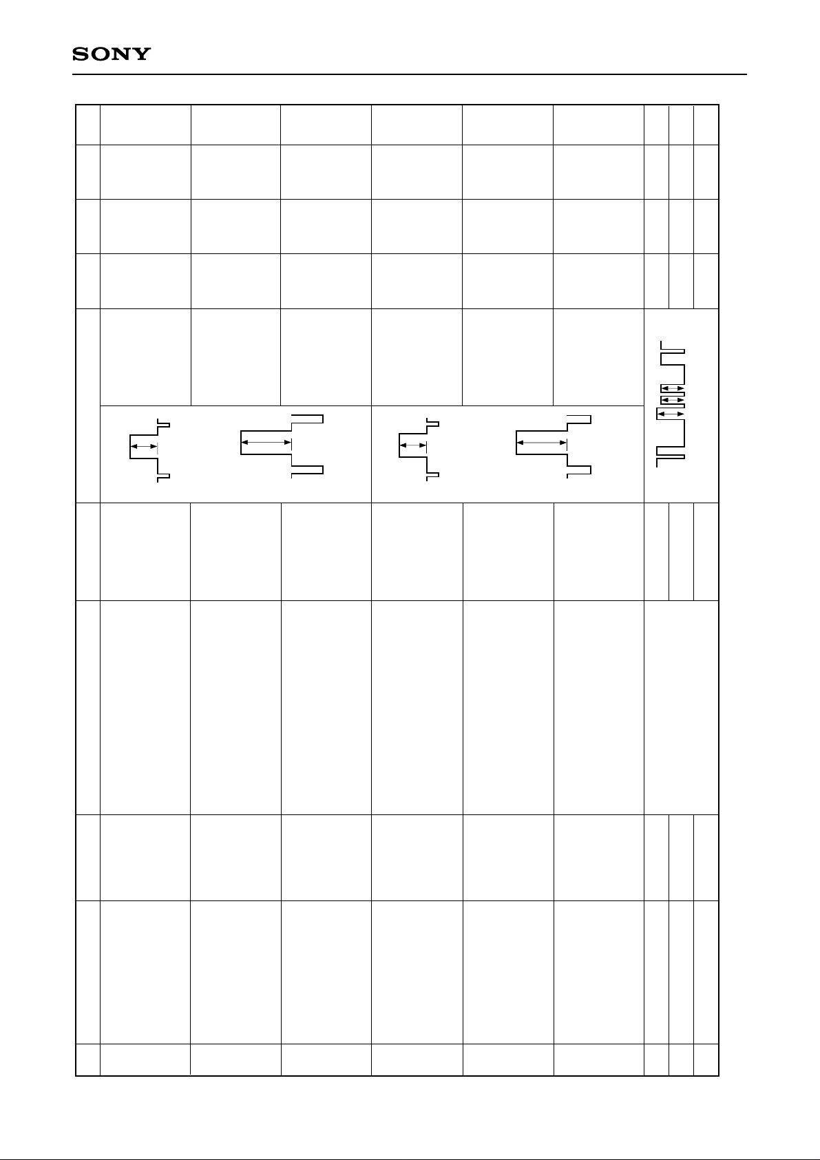
Electrical Characteristics
Setting conditions • Ta = 25°C, SVCC1, 2 = DVCC1, 2 = 9V, SGND1, 2 = DGND = 0V
No. Item
Sync deflection block items
Horizontal free-running
frequency
3
Horizontal sync pull-in
range
4
– 14 –
HD output pulse width
5
SCP
BLK output pulse width
SCP
6
7
BGP output pulse width
VDRIVE output
amplitude
8
VDRIVE output center
potential
9
Page 15

CXA2000Q
Unit
V
0.62
0.52
0.42
VEWp-p
Measurement contents Min. Typ. Max.
Measure the EWDRIVE output
Vp-p.
46: VSIN in
V
4.1
3.95
3.8
VEW dc
10.79ms
V
2.85
2.5
2.25
Output amplitude when a video
signal with an amplitude of
0.7Vp-p/100 IRE is input.
V1
V2
%
104
100
96
× 100
V1
Lin =
V2 × 2
dB
—
–30
—
f = 3.58MHz
Input fsc to CVIN.
Ratio of the fsc component of the
Yout amplitude when CTRAP = 1
against the Yout amplitude when
CTRAP = 0.
33
Measurement pins
Measurement conditions
SYNCIN: composite sync
VEWp-p
33
VEWdc
22, 24, 26
0.7Vp-p
/100 IRE
CVIN:
VRout1
22, 24, 26
100 IRE
50 IRE
CVIN:
Lin
22
CVIN:
fsc, 50 IRE
C-Trap3.58
TRAPOFF = 0/1
TRAP-F0 = 7h
No. Item Symbol
EWDRIVE output
amplitude
10
EWDRIVE output
center potential
11
Signal block items
R, G and B output
amplitude
12
– 15 –
R, G and B output
linearity
13
C-TRAP attenuation
(3.58MHz)
14
Page 16

CXA2000Q
Unit
dB
—
–30
—
Measurement contents Min. Typ. Max.
Input fsc to CVIN.
Ratio of the fsc component of the
Yout amplitude when CTRAP = 1
f = 4.43MHz
against the Yout amplitude when
CTRAP = 0.
50 IRE
f = 3MHz
V
1.15
0.95
0.75
Vvm
mV
570
510
440
OUT
–(R-Y)
Vr-y
mV
710
640
570
OUT
–(B-Y)
Vb-y
V
1.8
1.6
1.4
ROUT
Vcolr-y
V
1.5
1.3
1.1
Vcolb-y
BOUT
22
Measurement pins
CVIN:
Measurement conditions
fsc, 50 IRE
TRAPOFF = 0/1
TRAP-F0 = 7h
C-Trap4.43
49
burst fsc 300mVp-p
CVIN: 3MHz, 50 IRE
VMOFF = 0
4.43MHz PAL input
Vvm
3
450mVp-p
CIN
640mVp-p fsc + 90°
Vr-y
4
fsc + 0°, fsc + 180°
Vb-y
22
–(R-Y) IN: 525mVp-p
SUB-COLOR = 7h
PAL input: COLOR = 1Fh
Vcolr-y
24
–(B-Y) IN: 665mVp-p
PAL input: COLOR = 1Fh
Vcolb-y
No. Item Symbol
C-TRAP attenuation
(4.43MHz)
15
VM output
16
Color difference
–(R-Y) output
17
– 16 –
Color difference
–(B-Y) output
18
Color gain
–(R-Y)
19
Color gain
–(B-Y)
20
Page 17
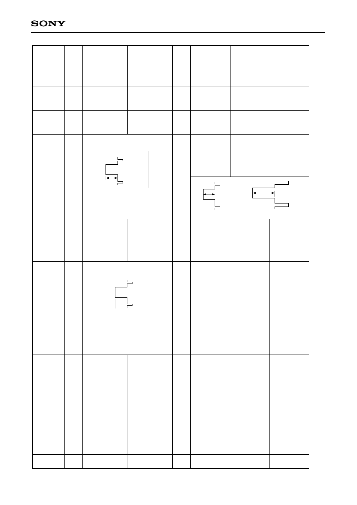
CXA2000Q
Unit
Measurement contents Min. Typ. Max.
deg
8
0
–8
dB
Hz
—
400
—
–35
—
–400
Confirm that the burst frequency
is pulled in at 3.58MHz ±400Hz.
%
98
96
94
Vp-p
ROUT, BOUT
%
106
104
102
× 100
× 100
Vp-p (DCOL = 1)
Vp-p (DCOL = 1)
Vp-p (DCOL = 0)
∆GdcolR =
∆GdcolB =
dB
–8.6
–9.6
–10.6
Vp-p (DCOL = 0)
Output amplitude ratio when the
R, G and BOUT YM = 1 and 0
V
2.25
2.05
1.85
VLR1out = Vout
IN
RGB1
V
2.25
2.05
1.85
VLG1out = Vout
out
R, G, B
V
2.25
2.05
1.85
VLB1out = Vout
—
—
—
Measurement pins
Measurement conditions
HUE = 1Fh, SUB – HUE = 7h
CVIN: Burst only
φoffset
KP
∆fAPC
22
CVIN: 100 IRE
∆GdcolR
24
D-COL = 0/1
∆GdcolB
22, 24, 26
∆GYM
22
YS1: 1V
RGB1IN: 0.7Vp-p
VLR1out
24
YS1: 1V
RGB1IN: 0.7Vp-p
VLG1out
26
YS1: 1V
RGB1IN: 0.7Vp-p
VLB1out
Hue center offset
Killer point
21
No. Item Symbol
22
APC pull-in range
23
Dynamic color
operation R output
24
Dynamic color
operation B output
25
– 17 –
YM gain
26
R output amplitude
during linear R1 input
G output amplitude
27
during linear G1 input
28
B output amplitude
29
during linear B1 input
Page 18
CXA2000Q
Unit
Measurement contents Min. Typ. Max.
V
2.25
2.05
1.85
VLR2out = Vout
IN
RGB2
V
2.25
2.05
1.85
VLG2out = Vout
out
R, G, B
V
2.25
2.05
1.85
VLB2out = Vout
IRE
75
67
58
VDRout = Vout
IN
RGB2
IRE
75
67
58
VDGout = Vout
out
R, G, B
IRE
75
67
58
VDBout = Vout
V
1.15
1.00
0.85
V
0.5
0.35
0.22
VIKG
V
0.5
0.35
0.22
VIKR VIKB
22
Measurement pins
Measurement conditions
YS2: 1V
RGB2IN: 0.7Vp-p
VLR2out
24
YS2: 1V
RGB2IN: 0.7Vp-p
VLG2out
26
YS2: 1V
RGB2IN: 0.7Vp-p
VLB2out
22
RGB2IN: 1.5Vp-p
VDRout
24
RGB2IN: 1.5Vp-p
VDGout
26
RGB2IN: 1.5Vp-p
VDBout
27
27
SYNCIN: composite sync
GCUTOFF = 0h
VIKR
VIKG
27
BCUTOFF = 0h
VIKB
R output amplitude
during linear R2
No. Item Symbol
30
input
G output amplitude
during linear G2
input
31
B output amplitude
during linear B2
32
input
R output amplitude
during digital R2
input
33
– 18 –
G output amplitude
during digital G2
input
34
B output amplitude
during digital B2
35
input
IK level R
IK level G
36
37
IK level B
38
Page 19
CXA2000Q
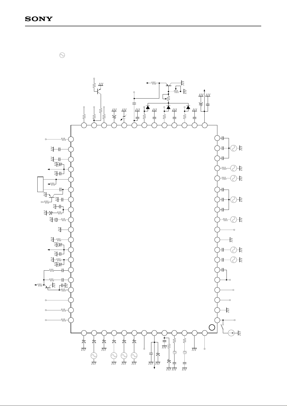
Electrical Characteristics Measurement Circuit
Signal sources are all GND unless otherwise specified in the Measurement conditions column of Electrical
Characteristics.
+9V
E/W
+9V
+9V
HP GEN.
HOFF
+9V
1k
VM
SCL
SDA
10k
1µ
330k
100
560
2.7k
500k
10k
100p
1µ
100
0.1µ
0.1µ
0.01µ
270
3.3k
220
220
(MPS)
0.01µ 47µ
4700p
0.01µ
8.2k
0.47µ 0.01µ 47µ
4700p
33
34
35
1
36
37
38
39
40
4142
43
2
44
45
46
47
48
49
50
51
VPROT
VDRV–
VDRV+
820
100 10k
100
VD+OUT/VPROT
CC
CC
VM
32
E-WOUT
VAGCSH
DV
HDOUT
L2FIL
AFCFIL
CERA
DGND
IREF
DV
VSFIL
VSIN
HSIN
SCL
SDA
BLHOLD
52
10µ
31
VD–OUT/VPROT
SAWOSC
AFCPIN/HOFF
SYNCOUT
CVIN
53
10µ
VTIM
VTIM
DCTRAN
CV IN
30
54
100
0.47µ
10µ
29
ABLFIL
YIN
55
10µ
Y IN
IK IN
1µ
B OUT
9V
28
ABLIN/VCOMP
EXT SYNC IN
56
0.001µ
27
IKIN
CIN
57
10µ
10µ
C IN
EXT SYNC IN
+9V
100
26
BOUT
TEST
58
0.01µ
TEST
51k
25
BSH
CC1
SV
59
G OUT
0.1µ
470p
24
GOUT
APCFIL
60
47µ
0.47µ
100
20k
15k
20k
0.1µ
23
GSH
X443
61
470
4.43MHz
15p
R OUT
100
22
ROUT
X358
62
1.5k
3.58MHz
15p
47µ
21
RSH
NC
63
0.1µ
+9V
0.01µ
20
CC2
B2IN
SV
G2IN
R2IN
YM
YS2
B1IN
G1IN
R1IN
YS1
SCPOUT
SGND2
–(B-Y) IN
–(R-Y) IN
YRET
YOUT
–(B-Y) OUT
–(R-Y) OUT
SGND1
SECAMREF
64
FSC OUT
FSC OUT
0.01µ
19
0.01µ
18
0.01µ
17
220
16
220
0.01µ
14 15
0.01µ
13
0.01µ
12
220
11
10
9
0.1µ
8
0.1µ
7
0.1µ
6
5
4
3
2
1
SCP OUT
Y OUT
–(B-Y) OUT
–(R-Y) OUT
SECAMREF
120µ
RGB2IN
YM
YS2
RGB1IN
YS1
–(B-Y) IN
–(R-Y) IN
– 19 –
+9V
Page 20
CXA2000Q
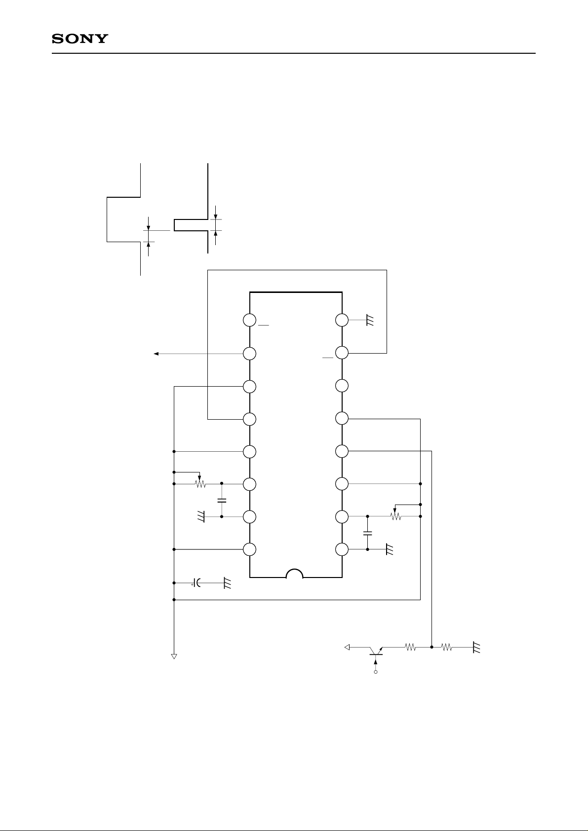
width12µs
delay 7µs
HDOUT
to AFCPIN
AFCPIN
10k
2000p
9
10
11
12
13
1415
16
2Q
2B
2A
DD
2Q
2T1
V
2CD
2T2
SS
TC4538BP
V
1Q
1Q
1B
1A
1CD
1T2
1T1
8
7
6
5
4
3
10k
2
2000p
1
HP GEN.
5V
47µ
– 20 –
9V
1k
from HDOUT
1k
Page 21
V parabola wave output
+9V
HD output
2.7k
100
HP outputHold-down input
0.1µ
10k
+9V
330k
100
2.2k
+9V
100p
VM
output
C BUS
2
I
input/output
2.2µ
470
CXA2000Q
V protect
signal input
V timing
pulse output
V sawtooth
wave outputs
100
100
VD+OUT/VPROT
32
100
33
0.1µ
34
2
∗
0.1µ
35
36
0.01µ 47µ
37
E-WOUT
VAGCSH
SAWOSC
DV
CC
1
HDOUT
0.1µ
38
4700p
0.01µ
5.6k
470
500k
1
∗
10k
1µ
0.47µ 47µ 0.01µ
0.0047µ
220
3.3k
220 220
L2FIL
39
AFCFIL
40
CERA
4142
DGND
IREF
43
DV
CC
2
44
VSFIL
45
VSIN
46
HSIN
47
48
49
50
51
SYNCOUT
VM
SCL
SDA
BLHOLD
52
4.7µ
10k
100
820
31
30
VTIM
29
ABLFIL
VD–OUT/VPROT
AFCPIN/HOFF
DCTRAN
CVIN
53
2.2µ
54
YIN
55
0.47µ
ABL/Vertical high
voltage fluctuation
compensation signal
input
Ik input
220
10µ
1k
10µ
1µ
28
27
IKIN
ABLIN/VCOMP
EXT SYNC IN
CIN
57
56
2.2µ
2.2µ
0.47µ
0.001µ
26
BOUT
TEST
58
0.01µ
100
25
BSH
CC1
SV
59
47µ
470p
RGB outputs
0.1µ
24
GOUT
APCFIL
60
0.47µ
100
0.1µ
23
GSH
X443
61
15k
510
4.433619MHz
15p
100
22
ROUT
X358
62
1.5k
3.579545MHz
15p
47µ
21
RSH
NC
63
0.1µ
CC2
SV
+9V
0.01µ
20
B2IN
G2IN
R2IN
YM
YS2
B1IN
G1IN
R1IN
YS1
SCPOUT
SGND2
–(B-Y) IN
–(R-Y) IN
YRET
YOUT
–(B-Y) OUT
–(R-Y) OUT
SGND1
SECAMREF
64
FSC OUT
1: Metal film resistor recommended
2: MPS capacitor recommended
∗
∗
0.01µ
19
0.01µ
18
0.01µ
Analog/digital
17
RGB inputs
16
220 220
YS2/YM
inputs
0.01µ
14 15
0.01µ
13
0.01µ
Analog RGB
12
inputs
220
YS1
11
input
10
9
0.1µ
Sand castle
pulse output
8
0.1µ
7
0.1µ
Color difference
outputs from
1H delay line
6
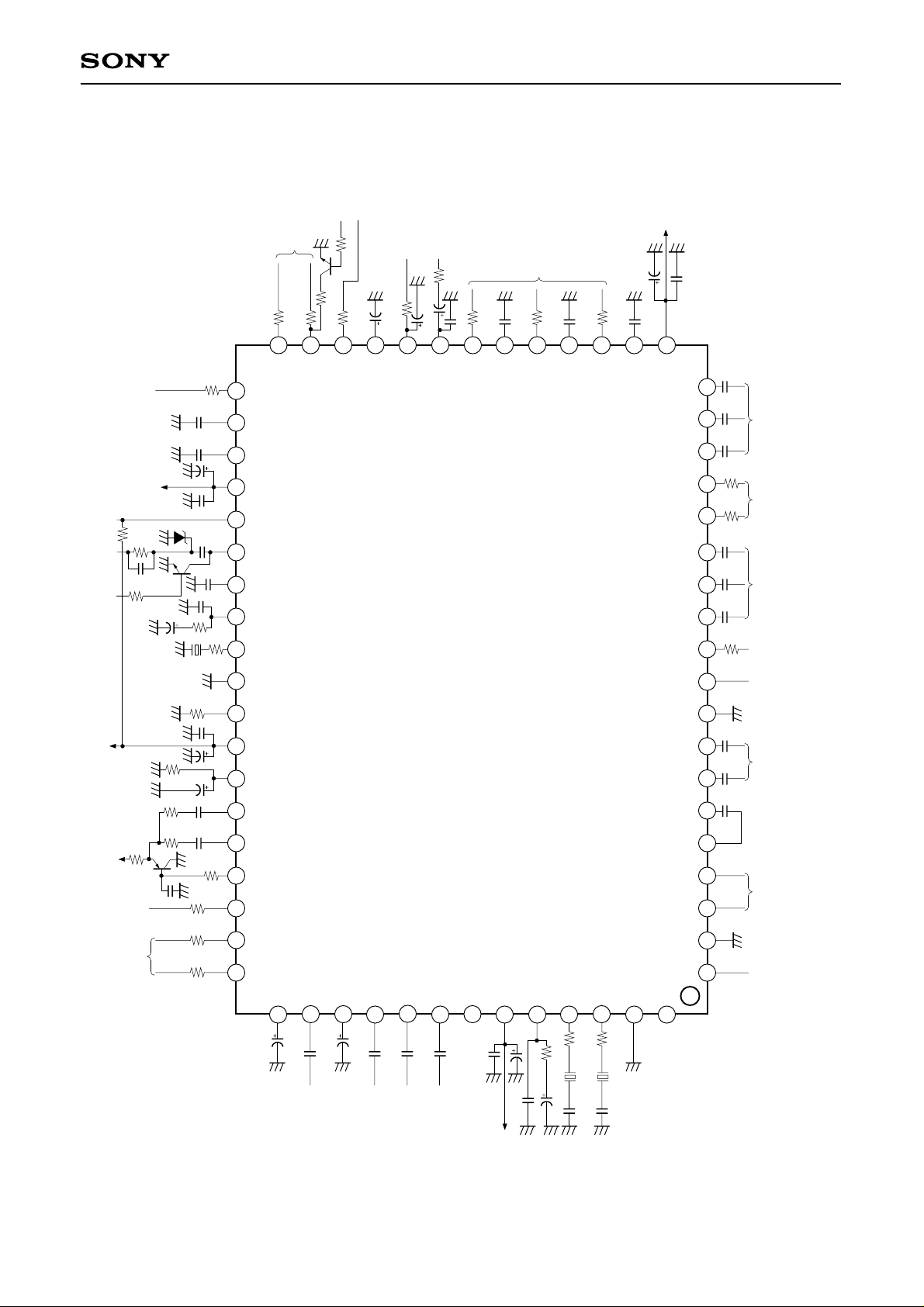
Application circuits shown are typical examples illustrating the operation of the devices. Sony cannot assume responsibility for
any problems arising out of the use of these circuits or for any infringement of third party patent and other right due to same.
5
4
3
Color difference
outputs for 1H
delay line
2
1
SECAM reference
input/output for
SECAM IC
Application Circuit
CV signal input
Y signal input
External sync
signal input
C signal input
– 21 –
+9V
Page 22
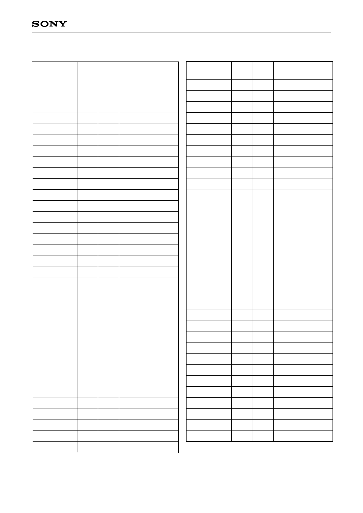
Electrical Characteristics Measurement Conditions "I2C Bus Register Initial Settings"
CXA2000Q
Register
name
PICTURE
TRAPOFF
VMOFF
HUE
DCTRAN
D-PIC
COLOR
TOT
BRIGHT
D-COL
SHARPNESS
PRE-OVER
COLOR SW
SUB-CONT
TRAP F0
SUB-COLOR
SUB-HUE
SUB-BRIGHT
GAMMA
G-DRIVE
AGING
B-DRIVE
INTERLACE
G-CUTOFF
B-CUTOFF
RON
GON
BON
PICON
VOFF
FHHI
CD-MODE
AKBOFF
No. of
bits
6
1
1
6
1
1
6
1
6
1
4
2
2
4
4
4
4
6
2
6
1
6
2
4
4
1
1
1
1
1
1
1
1
Initial
setting
3Fh
1h
1h
1Fh
0h
0h
1Fh
0h
1Fh
0h
7h
3h
0h
7h
7h
7h
7h
1Fh
0h
2Ah
0h
2Ah
0h
0h
0h
1h
1h
1h
1h
0h
0h
0h
0h
Description
Maximum value
TRAP off
VM off
Center value
DCTRAN off
DPIC off
Center value
TOT off
Center value
DCOL off
Center value
Maximum value
Automatic switching
Center value
Center value
Center value
Center value
Center value
Minimum value
Center value
AGING off
Center value
Interlace
Minimum value
Minimum value
R output on
G output on
B output on
Picture mute off
VD output on
FH normal
Automatic switching
AKB on
Register
name
V FREQ
V-POSITION
AFC-MODE
S-CORR
V-LIN
H-SIZE
REF-POSI
PIN-COMP
VBLKW
H-POSITOPN
PIN-PHASE
AFC-BOW
AFC-ANGLE
SCP BGR
SCP BGF
XTAL
EXT SYNC
CV/YC
V-ASPECT
ZOOM SW
HBLKSW
V-SCROLL
JMPSW
HSIZESW
UP-VLIN
LO-VLIN
LEFT-BLK
RIGHT-BLK
EHT H
EHT V
CORNER-PIN
YS1OFF
DL
No. of
bits
2
6
2
4
4
6
2
6
2
4
4
4
4
2
2
2
1
1
6
1
1
6
1
1
4
4
4
4
2
2
4
1
3
Initial
setting
0h
1Fh
1h
0h
7h
1Fh
3h
1Fh
0h
7h
7h
7h
7h
1h
1h
0h
0h
0h
0h
0h
0h
1Fh
0h
0h
0h
0h
7h
7h
0h
0h
7h
0h
3h
Description
Automatic switching
Center value
Low gain
Minimum value
Center value
Center value
Maximum value
Center value
Minimum value
Center value
Center value
Center value
Center value
Center value
Center value
Automatic switching
Internal sync
CV input
Minimum value
ZOOM SW off
HBLKSW off
Center value
JMPSW off
HSIZESW off
Minimum value
Minimum value
Center value
Center value
EHT H off
EHT V off
Center value
YS1 normal
Center value
V-SIZE
6
1Fh
Center value
– 22 –
Page 23
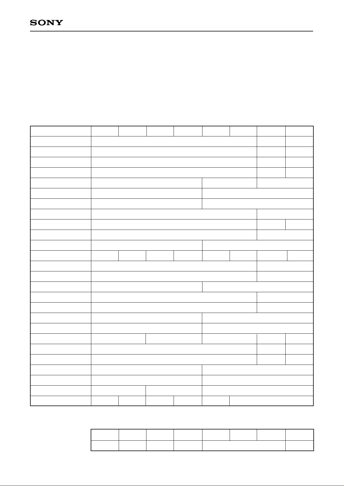
Definition of I2C Bus Registers
Slave Addresses
88h: Slave Receiver
89h: Slave Transmitter
Register Table
"∗": Undefined
Control Register
CXA2000Q
Sub Address
×××0 0 0 0 0 00 h
×××0 0 0 0 1 01 h
×××0 0 0 1 0 02 h
×××0 0 0 1 1 03 h
×××0 0 1 0 0 04 h
×××0 0 1 0 1 05 h
×××0 0 1 1 0 06 h
×××0 0 1 1 1 07 h
×××0 1 0 0 0 08 h
×××0 1 0 0 1 09 h
×××0 1 0 1 0 0A h
×××0 1 0 1 1 0B h
×××0 1 1 0 0 0C h
×××0 1 1 0 1 0D h
×××0 1 1 1 0 0E h
×××0 1 1 1 1 0F h
SHARPNESS
SUB-CONT
SUB-COLOR
SUB-BRIGHT
G-CUTOFF
V-POSITION
S-CORR
PICTURE
HUE
COLOR
BRIGHT
G-DRIVE
B-DRIVE
V-SIZE
H-SIZE
PRE-OVER
FHHIVOFFPICONBONGONRON
TRAPOFF
DC-TRAN
TOT
D-COL
TRAP F0
SUB-HUE
AGING 0
B-CUTOFF
CD-MODE
V-LIN
Bit0Bit1Bit2Bit3Bit4Bit5Bit6Bit7
VMOFF
D-PIC
∗
∗
COLOR SW
GAMMA
INTERLACE
AKBOFF
V-FREQ
AFC-MODE
REF-POSI
×××1 0 0 0 0 10 h
×××1 0 0 0 1 11 h
×××1 0 0 1 0 12 h
×××1 0 0 1 1 13 h
×××1 0 1 0 0 14 h
×××1 0 1 0 1 15 h
×××1 0 1 1 0 16 h
×××1 0 1 1 1 17 h
×××1 1 0 0 0 18 h
×××1 1 0 0 1 19 h
Status Register
PIN-COMP
H-POSITION
AFC-BOW
SCP BGR SCP BGF XTAL
V-ASPECT
V-SCROLL
UP-VLIN
LEFT-BLK
EHT H EHT V
∗∗ ∗
Bit7
H LOCK
Bit6
IKR
∗
Bit5
VNG
YS1 OFF DL
Bit4
XRAY
– 23 –
PIN-PHASE
AFC-ANGLE
LO-VLIN
RIGHT-BLK
CORNER-PIN
COLOR SYS
VBLKW
EXT SYNC
ZOOM SW
JMP SW
Bit1Bit2Bit3
CV/YC
HBLKSW
HSIZESW
Bit0
CV SYNC
Page 24

Description of Registers
Register name (No. of bits)
1. Video switch register
CV/YC (1) : CV input/YC input selector
0 = CV input selected
1 = YC input selected
EXT SYNC (1) : EXT SYNC selector switch
0 = Internal sync (CV or Y) selected
1 = EXT SYNC selected
2. Y signal block register
SUB-CONT (4) : Contrast gain control (Y gain control)
0h = –3.5dB
7h = 0dB
Fh = +2.5dB
CXA2000Q
TRAP-F0 (4) : Chroma trap f0 fine adjustment (Y block chroma trap current control)
0h = High
7h = Center
Fh = Low
SHARPNESS (4) : Sharpness gain control (Sharpness F0 3MHz)
0h = –6dB
7h = +2.5dB
Fh = +6.5dB
PRE-OVER (2) : Sharpness preshoot/overshoot ratio control
0h = 1:1 (PRE: OVER)
3h = 2:1
VM OFF (1) : Y signal output ON/OFF for VM
0 = ON
1 = OFF
TRAP OFF (1) : Y block chroma trap ON/OFF
0 = Trap ON
1 = Trap OFF
DL (3) : Y signal delay time control (80ns/step)
0h = Max.
7h = Min.
– 24 –
Page 25

DC-TRAN (1) : Y DC transmission ratio selector switch
0 = 100%
1 = 81%
D-PIC (1) : Y black expansion ON/OFF switch
0 = OFF
1 = ON Point of inflection: 30 IRE
3. C signal block register
TOT (1) : Chroma TOT filter band selector switch
0 = TOT — TRAP OFF
1 = TOT — TRAP ON (TRAP fo 2MHz)
COLOR (6) : Color gain control (Chroma gain control)
0h = Color OFF (–40dB or less)
1Fh = 0dB B output: 1.02Vp-p (I/O gain: +11dB, 0.285Vp-p input)
3Fh = +6dB
CXA2000Q
SUB-COLOR (4) : Color gain control (ACC reference level control)
0h = –5dB
7h = 0dB
Fh = +3dB
HUE (6) : Hue control (Phase control for chroma demodulation axis when SUB-HUE is 7h)
Control not possible for a PAL system.
0h = +35° Flesh color appears red.
1Fh = 0°
3Fh = –35° Flesh color appears green.
SUB-HUE (4) : Hue control (Phase control for chroma demodulation axis when HUE is 1Fh)
B-Y axis adjustable to 0°.
Control not possible for a PAL system.
0h = +10°
7h = 0°
Fh = –10°
XTAL (2) : XTAL selection setting switch
0h = Automatic identification
1h = Force to XTAL1 (3.58MHz)
2h = Force to XTAL2 (4.43MHz)
COLOR SW (2) : Color system setting
0h = Automatic identification
1h = Force to PAL
2h = Force to NTSC
3h = Force to SECAM
– 25 –
Page 26

4. RGB signal block register
PICTURE (6) : Picture gain control (RGB gain control)
0h = –14dB
3Fh = 0dB RGB output: 2.5Vp-p (I/O gain: +8dB, 1Vp-p input)
BRIGHT (6) : Bright control (RGB DC bias control)
0h = –440mV
1Fh = 0mV (–300mV for REF-P level)
3Fh = +450mV
SUB-BRIGHT (6) : Bright control (RGB DC bias control)
0h = –440mV
1Fh = 0mV (–300mV for REF-P level)
3Fh = +450mV
G-DRIVE (6) : Gch drive gain adjustment (Gch gain control)
0h = G/R –4.5dB
2Ah = G/R 0dB (G/R 0dB)
3Fh = G/R +1.5dB
CXA2000Q
B-DRIVE (6) : Bch drive gain adjustment (Bch gain control)
0h = B/R –4.5dB
2Ah = B/R 0dB (B/R 0dB)
3Fh = B/R +1.5dB
G-CUTOFF (4) : Gch cut-off adjustment (Gch reference pulse value control of IKIN pin input)
0h = +34%
7h = +81% (G/R)
Fh = +135%
B-CUTOFF (4): Bch cut-off adjustment (Bch reference pulse value control of IKIN pin input)
0h = +34%
7h = +81% (B/R)
Fh = +135%
D-COL (1) : Dynamic color ON/OFF switch
0 = Dynamic color OFF
1 = Dynamic color ON (R, Bch level control)
GAMMA (2) : Gamma control (RGB gamma correction amount control)
0h = Gamma OFF
3h = Gamma peak 17 IRE (at input 40 IRE), +400mV (at 2.5Vp-p OUT)
– 26 –
Page 27

REF-POSITION (2) : Reference pulse timing setting
0h = From rising edge of V TIM: Rch 22H, Gch 23H, Bch 24H
1h = From rising edge of V TIM: Rch 20H, Gch 21H, Bch 22H
2h = From rising edge of V TIM: Rch 18H, Gch 19H, Bch 20H
3h = From rising edge of V TIM: Rch 16H, Gch 17H, Bch 18H
PIC-ON (1) : ON/OFF switch for RGB output with a reference pulse
(Set to OFF mode at power-on.)
0 = RGB output OFF (All blanked status)
1 = RGB output ON
R ON (1) : ON/OFF switch for Rch video output without a reference pulse
(Operates when PIC ON = 1, set to OFF mode at power-on.)
0 = Rch video output OFF (Blanked status, reference pulse only output)
1 = Rch video output ON
G ON (1) : ON/OFF switch for Gch video output without a reference pulse
(Operates when PIC ON = 1, set to OFF mode at power-on.)
0 = Gch video output OFF (Blanked status, reference pulse only output)
1 = Gch video output ON
CXA2000Q
B ON (1) : ON/OFF switch for Bch video output without a reference pulse
(Operates when PIC ON = 1, set to OFF mode at power-on.)
0 = Bch video output OFF (Blanked status, reference pulse only output)
1 = Bch video output ON
AKB OFF (1) : AKB ON/OFF switch (Set to ON mode at power-on.)
0 = AKB ON
1 = AKB OFF (IK CLAMP, IK S/H and reference pulse fixed to OFF)
R, G and B cut-off adjustment at AKB OFF performed by voltage applied to RSH,
GSH and BSH pins, respectively.
YS1 OFF (1) : YS1 forced OFF mode/YS1 normal mode
0 = YS1 normal mode
1 = YS1 forced OFF mode
– 27 –
Page 28

5. Deflection block register
AFC-MODE (2) : AFC loop gain control (PLL between H SYNC and H VCO)
0h = H free run mode
1h = Small gain
2h = Medium gain
3h = Large gain
FH-HI (1) : H oscillator frequency fixation ON/OFF switch
(Set to ON mode at power-on.)
0 = H oscillator frequency fixation OFF AFC normal mode
1 = H oscillator frequency fixation ON Oscillator frequency fixed to maximum value
(approx. 16.2kHz).
V FREQ (1) : V frequency mode setting
0, 1h = Automatic identification
2h = Forced mode (50Hz)
3h = Forced mode (60Hz)
CXA2000Q
V OFF (1) : V sawtooth wave oscillation stop ON/OFF switch
(Set to OFF mode at power-on.)
0 = Oscillation stop OFF (V DRIVE– and V DRIVE+: normal output)
1 = Oscillation stop ON (V DRIVE– and V DRIVE+: DC output and DC value vary
according to V POSITION.)
CD-MODE (1) : V countdown system mode selector
(Set to automatic selection mode during power-on.)
0 = Non-standard signal mode, standard signal mode and no signal mode
automatically selected
1 = Fixed to non-standard signal mode
(V oscillator frequency is 55Hz during no signal mode "free run".)
VBLKW (2) : VBLK width control (Blanked pulses after reference pulse. Operates when
JMPSW = 1; blanked pulses after reference pulse fixed to 1H when JMPSW = 0.)
0h = 12H from Bch reference pulse
1h = 11H from Bch reference pulse
2h = 10H from Bch reference pulse
3h = 9H from Bch reference pulse
H-POSITION (4) : Horizontal position adjustment (HAFC phase control)
0h = 1µs delay Picture position shifts to right. (Picture delayed with respect to HD.)
7h = 0µs
Fh = 1µs advance Picture position shifts to left. (Picture advanced with respect to HD.)
V-POSITION (6) : Vertical position adjustment (V SAW output DC bias control)
0h = –0.09V Picture position drops, V DRIVE+ output DC Down.
1Fh = 0V Center potential: DC 3V
3Fh = +0.09V Picture position rises, V DRIVE+ output DC Up.
– 28 –
Page 29

CXA2000Q
V-SIZE (6) : Vertical amplitude adjustment (V SAW output gain control)
0h = –14% Vertical picture size decreases.
1Fh = 0% Amplitude: 1.23Vp-p, center potential: DC 3V when V-ASPECT is 2FH.
3Fh = +14% Vertical picture size increases.
V-LIN (4) : Vertical linearity adjustment (Gain control for V SAW secondary component)
0h = 115% (Bottom/top of picture) Top of picture compressed; bottom of picture
expanded.
7h = 100% (Bottom/top of picture)
Fh = 85% (Bottom/top of picture) Top of picture expanded; bottom of picture
compressed.
S-CORR (4) : Vertical S correction amount adjustment (V SAW secondary component gain control)
0h = Secondary component amplitude by adding sawtooth and other signals = 0
Fh = Secondary component amplitude by adding sawtooth and other signals = Maximum
AFC-BOW (4) : Vertical line bow compensation amount adjustment (Phase control according to
HAFC parabola wave)
0h = Top and bottom of picture delayed 500ns with respect to picture center.
7h = 0 ns
Fh = Top and bottom of picture advanced 500ns with respect to picture center.
AFC-ANGLE (4) : Vertical line slope compensation amount adjustment (Phase control according to
HAFC V SAW)
0h = Top of picture delayed 500ns, bottom of picture advanced 500ns with respect to
picture center.
7h = 0 ns
Fh = Top of picture advanced 500ns, bottom of picture delayed 500ns with respect to
picture center.
PIN-COMP (6) : Horizontal pin distortion compensation amount adjustment (V parabola wave gain
control)
0h = 0.10Vp-p Horizontal size for top/bottom of picture increases. (Compensation
amount minimum)
1Fh = 0.58Vp-p Amplitude, center potential: DC 4V when V-ASPECT is 2Fh
3Fh = 1.06Vp-p Horizontal size for top/bottom of picture decreases. (Compensation
amount maximum)
H-SIZE (6) : Horizontal amplitude adjustment (V parabola wave DC bias control)
0h = –0.5V Horizontal picture size decreases, EW-DRIVE output DC Down.
1Fh = 0V Amplitude: 0.58Vp-p, center potential: DC 4 V when V-ASPECT is 2Fh
3Fh = +0.5V Horizontal picture size increases, EW-DRIVE output DC Up.
EHT-H (2) : Horizontal high-voltage fluctuation compensation amount setting (DC adjustment for
parabolic output)
0h = 0V (Compensation amount when 1V is applied to ABL IN versus 8V applied
to ABL IN)
3h = –0.1V (Compensation amount when 1V is applied to ABL IN versus 8V applied
to ABL IN)
EHT-V (2) : Vertical high-voltage fluctuation compensation amount setting (V SAW output gain control)
0h = 0% (Compensation amount when 1V is applied to ABL IN versus 8V applied to
ABL IN)
3h = –7% (Compensation amount when 1V is applied to ABL IN versus 8V applied to
ABL IN)
INTERLACE (1) : Interlace mode and non-interlace display selector switch
0,1h = Interlace mode
2h = Interlace mode; 1/2H shift applied to EVEN lines
3h = Interlace mode; 1/2H shift applied to ODD lines
– 29 –
Page 30

CXA2000Q
PIN-PHASE (4) : Horizontal trapezoidal distortion compensation amount adjustment (V parabola wave
center timing control)
0h = 1.5ms advance Horizontal size for top of picture increases; horizontal size for
bottom of picture decreases.
7h = 0ms 8.9ms from 4VDC VTIM
Fh = 1.5ms delay Horizontal size for top of picture decreases; horizontal size
for bottom of picture increases.
CORNER-PIN (4) : Horizontal pin distortion compensation amount adjustment for top/bottom of picture
(V parabola wave top/bottom gain control)
0h = –0.2V Horizontal size for top/bottom of picture decreases.
(compensation amount maximum)
7h = 0V (0.7Vp-p 4:3 mode)
Fh = +0.2V Horizontal size for top/bottom of picture increases.
(compensation amount minimum)
V-ASPECT (6) : Aspect ratio control. (Gain control for sawtooth wave)
0h = 75% 16:9 CRT full
2Fh = 100% 4:3 CRT full, amplitude: 1.23Vp-p
3Fh = 112%
ZOOM SW (1) : Zoom mode ON/OFF switch for 16:9 CRT (25% of video cut)
0 = Zoom OFF Sawtooth wave amplitude: 1.23Vp-p
1 = Zoom ON Sawtooth wave amplitude: 70%
HBLKSW (1) : HBLK width control ON/OFF switch during 4:3 software full display mode on a 16:9
CRT
0 = Control OFF HBLK pulse generated from HPIN.
1 = Control ON HBLK pulse generated as pulse generated from HPIN or as
pulse generated from HVCO and width adjusted.
Width adjustment is performed by the LEFT-BLK and
RIGHT-BLK registers.
V-SCROLL (6) : Vertical picture scroll control during zoom mode on a 16:9 CRT
(DC component added to sawtooth wave AGC output to control ZOOMSW cut
timing.)
0h = –0.2V Scrolled toward top of screen by 32H and top of picture zoomed.
1Fh = 0V
3Fh = +0.2V Scrolled toward bottom of screen by 32H and bottom of picture zoomed.
JUMPSW (1) : Reference pulse jump mode ON/OFF switch (In addition to V-ASPECT control, sawtooth
wave gain control performed for 100% of VBLK interval and 67% of picture interval)
0 = Jump mode OFF
1 = Jump mode ON
On a 4:3 CRT, jump mode expands the sawtooth wave amplitude to 112% with VASPECT; on a 16:9 CRT, jump mode compresses the sawtooth wave amplitude to
75% with V-ASPECT. The V blanking width is expanded at both the top and bottom
of the picture. Blanking for the bottom of the picture starts 251H after VTIM, and
blanking for the top of the picture can be varied as the blanking width after the
reference pulse from the VBLKW register.
HSIZESW (1) : Lowers the E-W OUT DC level (during H-SIZE compression)
0 = Normal
1 = –1.35V
– 30 –
Page 31

CXA2000Q
UP-VLIN (4) : Vertical linearity adjustment for top of picture (Secondary component gain control for
sawtooth wave added to sawtooth wave AGC output)
0h = 100% (Bottom/top of picture)
Fh = 115% (Bottom/top of picture) Top of picture compressed.
LO-VLIN (4) : Vertical linearity adjustment for bottom of picture (Tertiary component gain control
for sawtooth wave added to sawtooth wave AGC output)
0h = 100% (Bottom/top of picture)
Fh = 85% (Bottom/top of picture) Bottom of picture compressed.
LEFT-BLK (4) : HBLK width control for the left side of picture when HBLKSW = 1 (Phase control for
timing pulse generated from HVCO)
0h = +1.3µs HBLK width maximum
7h = 0µs Center HBLK: 13µs
Fh = –1.3µs HBLK width minimum
RIGHT-BLK (4) : HBLK width control for the right side of picture when HBLKSW = 1 (Phase control for
timing pulse generated from HVCO)
0h = +1.3µs HBLK width maximum
7h = 0µs Center HBLK: 13µs
Fh = –1.3µs HBLK width minimum
SCP BGR (2) : Controls the phase of the rising edge of the burst pulse in sand castle pulse output
(0.4µs/step)
0h = +0.4µs
1h = Center
3h = –0.8µs
SCP BGF (2) : Controls the phase of the falling edge of the burst pulse in sand castle pulse output
(0.4µs/step)
0h = +0.4µs
1h = Center
3h = –0.8µs
6. Other
AGING (1) : White output aging mode ON/OFF switch
(Takes priority over RGB ON and PIC ON control. Set to OFF mode at power-on.)
0 = Aging mode OFF
1 = Aging mode ON (When there is no input signal, a 60 IRE flat signal is output
from the Y block)
– 31 –
Page 32

7. Status register
HLOCK (1) : Lock status between H SYNC and H VCO
0 = HVCO free run status
1 = Locked to H SYNC
IKR (1) : AKB operation status
0 = REF-P at Ik small and AKB loop unstable.
1 = REF-P at Ik sufficient and AKB loop stable.
VNG (1) : Signal input status to V PROT pin
0 = No V PROT input
1 = V PROT input (In this case, the RGB output is blanked.)
XRAY (1) : Signal input status to XRAY control pin (HOFF pin)
0 = No XRAY control input
1 = XRAY control input (In this case, the RGB output is blanked.)
CXA2000Q
COLOR SYS (3) : Color system status
0h = —
1h = —
2h = NO STANDARD
3h = SECAM
4h = 3.58MHz NTSC
5h = 4.43MHz NTSC
6h = 3.58MHz PAL
7h = 4.43MHz PAL
CV SYNC (1) : CV input SYNC SEP result
When VIDEO is input to CVIN, "1" is returned when the SYNC level is 100mV or
more (standard: 300mV)
0 = No SYNC
1 = SYNC
– 32 –
Page 33

CXA2000Q
Description of Operation
1. Power-on sequence
The CXA2000Q does not have an internal power-on sequence. Therefore, power-on sequence is all controlled
by the set microcomputer (I2C bus controller).
1) Power-on
The IC is reset and the RGB outputs are all blanked. Hdrive starts to oscillate, but oscillation is at the
maximum frequency (16kHz or more) and is not synchronized to the input signal. Output of vertical signal
VTIM starts, but Vdrive is DC output. Bus registers which are set by power-on reset are as follows.
AGING = 0: All white output aging mode OFF
RON = 0: Rch video blanking ON
GON = 0: Gch video blanking ON
BON = 0: Bch video blanking ON
PICON = 0: RGB all blanking ON
VOFF = 1: VDRIVE output stopped mode
VFREQ = 0: Automatic identification mode (identification starts at 50Hz)
FHHI = 1: H oscillator maximum frequency mode
HSIZESW = 0: Normal
CD-MODE = 0: Automatic selection mode of the countdown mode
AKBOFF = 0: AKB mode
2) Bus register data transfer
The register setting sequence differs according to the set sequence. Register settings for the following
sequence are shown as an example.
Set sequence CXA2000Q register settings
Power-on Reset status in 1) above.
↓↓
Degauss Reset status in 1) above.
The CRT is degaussed in the completely darkened condition.
↓↓
VDRIVE oscillation The IC is set to the power-on initial settings. (See the following page.)
A sawtooth wave is output to VDRIVE and the IC waits for the vertical
deflection to stabilize. The HDRIVE oscillator frequency goes to the standard
frequency.
↓↓
AKB operation start PICON is set to 1 and a reference pulse is output from Rout, Gout and Bout.
Then, the IC waits for the cathode to warm up and the beam current to start
flowing.
↓↓
AKB loop stable Status register IKR is monitored.
IKR = 0: No cathode current
IKR = 1: Cathode current
Note that the time until IKR returns to 1 differs according to the initial status
of the cathode.
↓↓
Video output RON, GON and BON are set to 1 and the video signal is output from Rout,
Gout and Bout.
– 33 –
Page 34
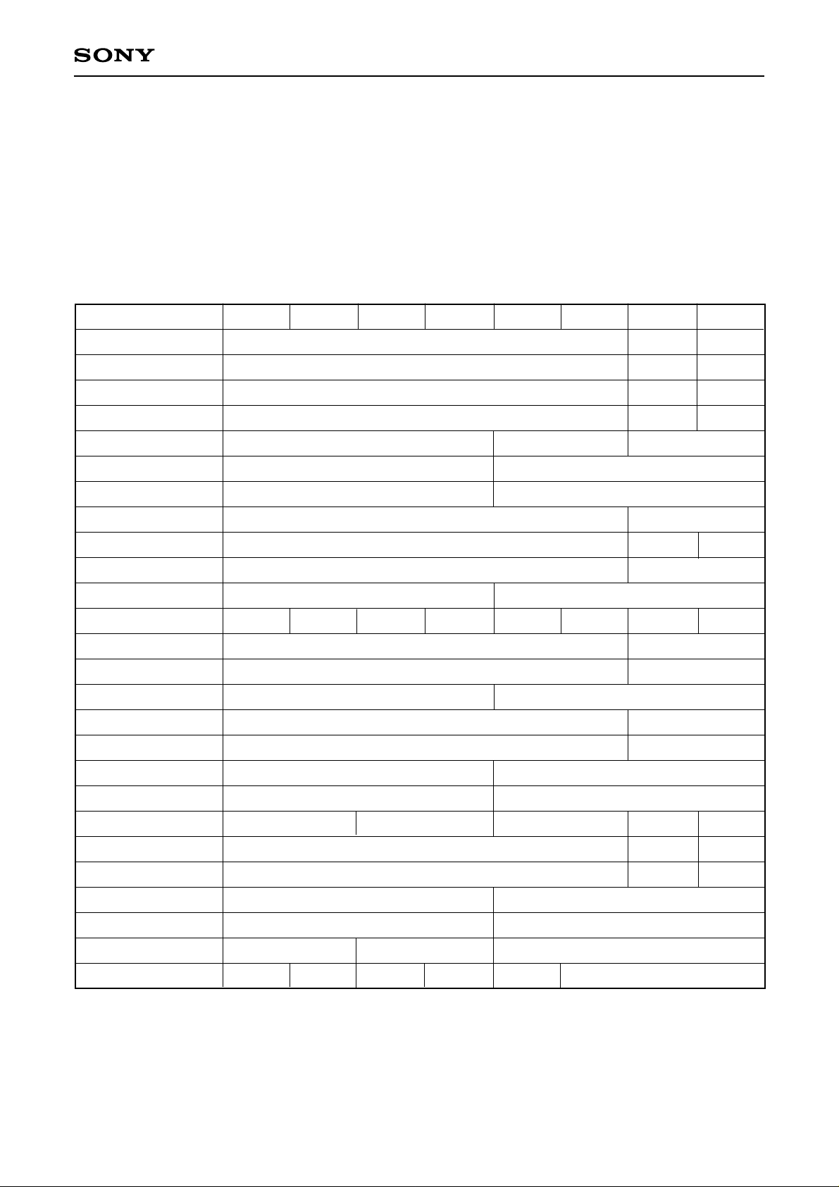
CXA2000Q
I2C bus power-on initial settings
The initial settings listed here for power-on when VDRIVE starts to oscillate are reference values; the actual
settings may be determined as needed according to the conditions under which the set is to be used.
Register Table
"∗" Undefined
Control Register
Sub Address
×××0 0 0 0 0 00 h
×××0 0 0 0 1 01 h
×××0 0 0 1 0 02 h
×××0 0 0 1 1 03 h
×××0 0 1 0 0 04 h
×××0 0 1 0 1 05 h
×××0 0 1 1 0 06 h
×××0 0 1 1 1 07 h
×××0 1 0 0 0 08 h
×××0 1 0 0 1 09 h
×××0 1 0 1 0 0A h
×××0 1 0 1 1 0B h
×××0 1 1 0 0 0C h
×××0 1 1 0 1 0D h
×××0 1 1 1 0 0E h
×××0 1 1 1 1 0F h
Bit0Bit1Bit2Bit3Bit4Bit5Bit6Bit7
1
0
0
0
0
0
0
0
0
0
0
0
0
0
0
0
1
1
1
1
1
1
1
1
1
1
1
0
1
1
1
1
1
1
1
1
1
1
1
1
1
1
1
0
1
1
1
1
1
1
1
1
1
1
1
1
1
1
1
0
1
1
1
1
1
1
1
1
0
0
0
1
1
1
0
0
1
1
0
1
1
1
1
1
0
1
1
1
1
1
1
0
1
1
1
1
0
0
0
1
0
1
1
0
0
0
1
0
0
1
1
0
0
1
∗
∗
0
1
1
0
0
0
1
0
0
0
1
0
×××1 0 0 0 0 10 h
×××1 0 0 0 1 11 h
×××1 0 0 1 0 12 h
×××1 0 0 1 1 13 h
×××1 0 1 0 0 14 h
×××1 0 1 0 1 15 h
×××1 0 1 1 0 16 h
×××1 0 1 1 1 17 h
×××1 1 0 0 0 18 h
×××1 1 0 0 1 19 h
0
0
0
0
0
0
0
0
0
∗
1
1
1
1
0
1
1
1
0
∗
1
1
1
0
0
1
1
1
1
∗
1
1
1
1
0
1
1
1
1
∗
1
0
0
0
0
1
0
1
0
0
1
1
1
0
0
1
1
1
1
0
0
1
1
0
1
0
1
1
1
1
0
1
1
0
1
0
1
1
1
1
– 34 –
Page 35

CXA2000Q
3) Power-on initial settings
The initial settings listed here for power-on when VDRIVE starts to oscillate are reference values; the actual
settings may be determined as needed according to the conditions under which the set is to be used.
PICTURE = 3Fh Max (User Control)
TRAP OFF = 0 Chroma Trap ON
VM OFF = 0 VM out ON
HUE = 1Fh Center (User Control)
DC-TRAN = 0 Y DC transmission ratio 100%
D-PIC = 1 Y black expansion ON
COLOR = 1Fh Center (User Control)
TOT = 0 Chroma low frequency increased
BRIGHT = 1Fh Center (User Control)
D-COL = 1 Dynamic Color ON
SHARPNESS = 7h Center (User Control)
PRE-OVER = 0 Sharpness pre/over ratio 1:1
COLOR SW = 0 AUTO
SUB-CONT = 7h Center (Adjust)
TRAP F0 = 7h Center (Adjust)
SUB-COLOR = 7h Center (Adjust)
SUB-HUE = 7h Center (Adjust)
SUB-BRIGHT = 1Fh Center (Adjust)
GAMMA = 0 Gamma OFF
G-DRIVE = 1Fh Center (Adjust)
AGING = 0 Aging Mode OFF
B-DRIVE = 1Fh Center (Adjust)
INTERLACE = 0 INTERLACE mode
G-CUTOFF = 7h Center (Adjust)
B-CUTOFF = 7h Center (Adjust)
RON = 0 Rch video output OFF
GON = 0 Gch video output OFF
BON = 0 Bch video output OFF
PICON = 0 RGB all blanked
VOFF = 0 Vdrive oscillation
FHHI = 0 Horizontal oscillator frequency standard
CD-MODE = 0 V countdown auto mode
AKBOFF = 0 AKB ON
V-SIZE = 1Fh Center (Adjust)
V-FREQ = 0 AUTO
V-POSITION = 1Fh Center (Adjust)
AFC-MODE = 2 Center
S-CORR = 7h Center (Adjust)
V-LIN = 7h Center (Adjust)
H-SIZE = 1Fh Center (Adjust)
REF-POSI = 0
PIN-COMP = 1Fh Center (Adjust)
VBLKW = 0
– 35 –
Page 36

(Power-on initial settings cont.)
H-POSITION = 7h Center (Adjust)
PIN-PHASE = 7h Center (Adjust)
AFC-BOW = 7h Center (Adjust)
AFC-ANGLE = 7h Center (Adjust)
SCP BGR = 1 Center
SCP BGF = 1 Center
XTAL = 0 AUTO
EXT SYNC = 0 Internal SYNC
CV/YC = 0 CV input
V-ASPECT = 0h 16:9 CRT Full Mode
ZOOMSW = 1 16:9 CRT
HBLKSW = 1 Hblk width adjust ON
V-SCROLL = 1Fh Center (User Control)
JMPSW = 0 16:9 CRT Full Mode
HSIZE SW = 0 Normal
UP-VLIN = 7h 16:9 CRT Full Mode
LO-VLIN = 7h 16:9 CRT Full Mode
LEFT-BLK = Fh Hblk width Min.
RIGHT-BLK = Fh Hblk width Min.
EHT-H = 0 Hdrive high-voltage compensation OFF
EHT-V = 3 Vdrive high-voltage compensation amount maximum
CORNERPIN = 7h Center (Adjust)
YS1 OFF = 0 Normal
DL = 3 Normal (Adjust)
CXA2000Q
2. Various mode settings
The CXA2000Q contains bus registers for deflection compensation which can be set for various wide modes.
Wide mode setting registers can be used separately from registers for normal picture distortion adjustment,
and once deflection adjustment has been performed in full mode, wide mode settings can be made simply by
changing the corresponding register data.
• VDRIVE signal picture distortion adjustment registers
V-SIZE, V-POSITION, S-CORR, V-LIN
• E/WDRIVE signal picture distortion adjustment registers
H-SIZE, PIN-COMP, PIN-PHASE, CORNER-PIN
• Wide mode setting registers
V-ASPECT, ZOOMSW, HBLKSW, V-SCROLL, JMPSW, HSIZESW, UP-VLIN, LO-VLIN,
LEFT-BLK, RIGHT-BLK
– 36 –
Page 37

CXA2000Q
Examples of various modes are listed below. These modes are described using 570 (NTSC: 480) lines as the
essential number of display scanning lines. Wide mode setting register data is also listed, but settings may
differ slightly due to IC variation. The standard setting data differs for 16:9 CRTs and 4:3 CRTs.
Register 16:9 CRT 4:3 CRT
V-ASPECT 0h 2Fh
V-SCROLL 1Fh 1Fh
ZOOMSW 1 0
UP-VLIN 0h 0h
LO-VLIN 0h 0h
JMPSW 0 0
HSIZESW 0 0
HBLKSW 0 0
LEFT-BLK 7h 7
RIGHT-BLK 7h 7h
1) 16:9 CRT full mode
This mode reproduces the full 570 (NTSC:480) lines on a 16:9 CRT. 4:3 images are reproduced by stretching
the picture to the left and right.
Normal images are compressed vertically, but 16:9 images can be reproduced in their original 16:9 aspect
ratio with a video source which compresses (squeezes) 16:9 images to 4:3 images. The register settings are
the 16:9 CRT standard values.
2) 16:9 CRT normal mode
In this mode, 4:3 images are reproduced without modification. A black border appears at the left and right of
the picture. In this mode, the H deflection size must be compressed by 25% compared to full mode. The
CXA2000Q permits compression with a register (HSIZESW) that compresses the H size by 25%. Because
excessive current flows to the horizontal deflection coil in this case, adequate consideration must be given to
the allowable power dissipation, etc., of the horizontal deflection coil in the design of the set. In addition, this
concern can also be addressed through measures taken external to the IC, such as by switching the horizontal
deflection coil. Full mode should be used when using memory processing to add a black border to the video
signal.
H blanking of the image normally uses the flyback pulse input to AFCPIN (Pin 38). However, the blanking
width can be varied according to the control register setting when blanking is insufficient for the right and left
black borders.
The following three settings are added to the 16:9 CRT standard values for the register settings.
HBLKSW = 1
LEFT-BLK = Adjustment value
RIGHT-BLK = Adjustment value
The H angle of deflection also decreases, causing it to differ from the PIN compensation amount during H size
full status. Therefore, in addition to the wide mode registers, PIN-COMP must also be readjusted only for this
mode.
3) 16:9 CRT zoom mode
In this mode, 4:3 images are reproduced by enlarging the picture without other modification. The top and
bottom of normal 4:3 images are lost, but almost the entire picture can be reproduced for vista size video
software, etc. which already has black borders at the top and bottom. The enlargement ratio can be controlled
by the V-ASPECT register, and enlarging the picture by 33% compared to full mode allows zooming to be
performed for 4:3 images without distortion. In this case, the number of scanning lines is reduced to 430 lines
compared to 570 lines for full mode. The zooming position can be shifted vertically by the V-SCROLL register.
V blanking of the image normally begins from V sync and continues for 2H after the AKB reference pulse, and
the top and bottom parts are also blanked during this mode.
Adjust the following two registers with respect to the 16:9 CRT standard values for the register settings.
V-ASPECT = 2Fh
V-SCROLL = 1Fh or user control
– 37 –
Page 38

CXA2000Q
4) 16:9 CRT subtitle-in mode
When CinemaScope size images which have black borders at the top and bottom of the picture are merely
enlarged with the zoom mode in 3) above, subtitles present in the black borders may be lost. Therefore, this
mode is used to super-compress only the subtitle part and reproduce it on the display.
Add the LO-VLIN adjustment to the zoom mode settings for the register settings.
V-ASPECT = 2Fh
V-SCROLL = 1Fh or user control
LO-VLIN = Adjustment value
The LO-VLIN register causes only the linearity at the bottom of the picture to deteriorate. Therefore, UP-VLIN
should also be adjusted if the top and bottom of the picture are to be made symmetrical. Since the picture is
compressed vertically, the number of scanning lines exceeds 430 lines.
5) 16:9 CRT V compression mode
This mode is used to reproduce two 4:3 video displays such as for PandP. The V size must be compressed to
67% in order to reproduce two displays on a 16:9 CRT without distortion using 480 scanning lines, and this can
be set by JMPSW. Compression is performed after the AKB reference pulse, so the reference pulse remains in
the overscan position. The V blanking width after the reference pulse becomes larger than normal and can be
varied by the VBLKW register. During this mode, the bottom V blanking width is also expanded to 3H wider
than normal so that the bottom of the picture is not overscanned.
16:9 CRT standard values are used with only the JMPSW setting changed for the register settings.
JMPSW = 1
6) 16:9 CRT wide zoom mode
This mode reproduces 4:3 video software naturally on wide displays by enlarging 4:3 images without other
modification and compressing the parts of the image which protrude from the picture into the top and bottom
parts of the picture. The display enlargement ratio is controlled by V-ASPECT, and the compression ratios at
the top and bottom of the picture are controlled by UP-VLIN and LO-VLIN.
Adjust the following three registers with respect to the 16:9 CRT standard values for the register settings.
V-ASPECT = Adjustment value
UP-VLIN = Adjustment value
LO-VLIN = Adjustment value
7) 4:3 CRT normal mode
This is the standard mode for 4:3 CRTs.
The register settings are the 4:3 CRT standard values.
8) 4:3 CRT V compression mode
This mode is used to reproduce M-N converter output consisting of 16:9 images expanded to a 4:3 aspect ratio
and other squeezed signals without distortion on a 4:3 CRT. The V size must be compressed to 75% in order
to reproduce a 4:3 squeezed signal at a 16:9 aspect ratio without any distortion. Compressing the V size with
the JMPSW register used in mode 5) above, compresses the V size to 67%. Therefore, V-ASPECT is set to
enlarge the V size by 8%. AKB reference pulse handling and V blanking are the same as for mode 5) above.
4:3 CRT standard values are used with the V-ASPECT and JMPSW settings changed for the register settings.
V-ASPECT = 3Fh
JMPSW = 1
– 38 –
Page 39
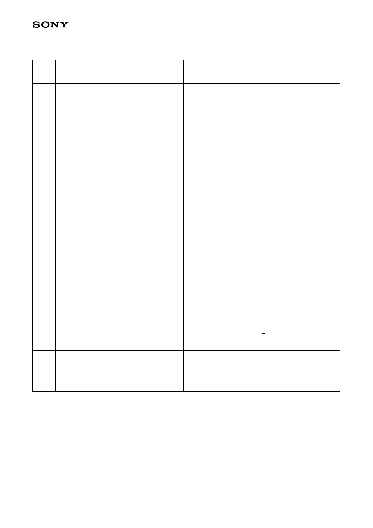
Mode Settings
CXA2000Q
Setting CRT SIZE
1)-1
1)-2
2)
3)
4)
16:9
16:9
16:9
16:9
16:9
SOFT SIZE
16:9
4:3
4:3
4:3
4:3
(16:9
+ subtitle
area)
MODE NAME I2C BUS REGISTER
16:9 CRT full
Wide full
V-ASPECT = 0h: V size 75%
V-ASPECT = 0h: V size 75%
V-ASPECT = 0h: V size 75%
HBLKSW = 1h: HBLK width adjustment ON
16:9 CRT normal
LEFT-BLK = Adjustable
RIGHT-BLK = Adjustable
PIN-COMP = Adjustable
(External support: H-DY H amplitude 75%)
V-ASPECT = 2Fh: V size 100%
ZOOMSW = 1h: Zoom ON
V size limited at 75%
16:9 CRT zoom
V-SCROLL = 0h: Zoom bottom of video image
1Fh: Zoom center of video image
3Fh: Zoom top of video image
Adjustable: Open to user
V-ASPECT = 2Fh: V size 100%
UP-VLIN = Adjustable: Slightly compresses top of
16:9 CRT with
subtitle area on
LO-VLIN = Adjustable: Significantly compresses
video image
bottom of video image
ZOOMSW 1h: V size limited at 75%
(V-SCROLL = Adjustable)
V-ASPECT = 0h: V size 75%
JMPSW = 1h: Reference pulse skipping ON
5)
16:9
4:3
16:9 CRT V
compression
V size compressed 67% after the reference pulse
(compressed to 50% total)
VBLKW = Adjustable: VBLK width expanded at
top and bottom of video image
V-ASPECT = Adjustable: V size 90%
6)
7)
16:9
4:3
4:3
4:3
16:9 CRT wide
zoom
4:3 CRT normal
UP-VLIN = Adjustable:
LO-VLIN = Adjustable:
(S-CORR = Adjustable):
Compression of top and
bottom of video image
V-ASPECT = 2Fh: V size 100%
V-ASPECT = 3Fh: V size 112%
JMPSW = 1h: Reference pulse skipping ON
(compressed to 75% total)
VBLKW = Adjustable: VBLK width expanded at
8)
4:3
16:9
4:3 CRT V
compression
top and bottom of video image
∗
The amount of picture distortion compensation in a vertical direction position of the CRT does not change in
response to the above modes; as a result, the initial values of each picture distortion register can be used as
is.
– 39 –
Page 40

CXA2000Q
3. Signal processing
The CXA2000Q is comprised of sync signal processing, H deflection signal processing, V deflection signal
processing, and Y/C/RGB signal processing blocks, all of which are controlled by the I2C bus.
1) Sync signal processing
Pin 48 (SYNC OUT) outputs at 2Vp-p either the internal signal (CVIN/YIN) selected by the internal video
switch, or the external sync signal input from Pin 56 (EXT SYNC IN).
This selection is controlled by the I2C bus. The signal output from Pin 48 is buffered by a PNP Tr. and is then
input to HSIN (Pin 47) or VSIN (Pin 46) through a suitable filter.
The Y signals input to Pins 46 and 47 are sync separated by the horizontal and vertical sync separation
circuits. The resulting horizontal sync signal and the signal (FH = 15625Hz or 15734Hz) obtained by frequency
dividing the 32FH-VCO output using the ceramic oscillator (frequency 500kHz or 503.5kHz) by 32 are phasecompared, the AFC loop is constructed, and an H pulse synchronized with the H sync is generated inside the
IC. Adjustment of the H oscillator frequency is unnecessary. When the AFC is locked to the H sync, 1 is output
to the status register (HLOCK) and that can be used to detect the presence of the video signal.
The vertical sync signal is sent to the V countdown block where the most appropriate window processing is
performed to obtain V sync timing information which resets the counter. AKB and other V cycle timing are then
generated from this reset timing.
2) H deflection signal processing
The H pulse obtained through sync processing is phase-compared with the H deflection pulse input from Pin
38 to control the phase of the HDRIVE output and the horizontal position of the image projected on the CRT.
In addition, the compensation signal generated from the V sawtooth wave is superimposed, and the vertical
picture distortion is compensated.
The H deflection pulse is used to H blanking of the video signal. When the pulse input from Pin 38 has a
narrow width, the pulse generated by the IC can be added to the H deflection pulse and used as the H
blanking pulse (HBLKSW).
Pin 38 is normally pulse input, but if the pin voltage drops to the GND level, HDRIVE output stops and 1 is
output to the status register (XRAY). To release this status, turn the power off and then on again.
3) V deflection signal processing
The V sawtooth wave is generated at the cycle of the reset pulse output from the countdown system. After
performing wide deflection processing for this sawtooth wave, picture distortion adjustment is performed by the
VDRIVE and E/WDRIVE function circuits and the signal is output as the VDRIVE and E/WDRIVE signals.
4) Y signal processing
Either CVIN, input from Pin 53, or YIN, output from Pin 55, is selected by the video switch and then is passed
to the Y signal processing circuit as the Y signal. The input level is 1Vp-p.
The Y signal passes through the subcontrast control, the trap for eliminating the chroma signal, the delay line,
the sharpness control, the clamp and the black expansion circuits, and is then output to Pin 5 as YOUT. The
differential waveform of the Y signal, advanced for about 200ns from YOUT is output from Pin 49 as the VM
signal. The delay time is set by the bus register (DL).
When CVIN is selected, the trap is on; when YIN is selected, the trap is off.
The f0 of the internal filter is automatically adjusted within the IC. Because the f0 of the filter is not specified
when the color killer function is operating, turn the trap off if there are any difficulties. In addition, the f0 of the
trap will be affected slightly by variations among IC, so fine adjustment through the I2C bus (TRAP-F0) may be
required.
– 40 –
Page 41

CXA2000Q
5) C signal processing
The CVBS signal or chroma signal (specified input level: burst level of 300mVp-p) selected by the video switch
passes through the ACC, TOT, chroma amplifier and demodulation circuits, becomes the R-Y and B-Y color
difference signals, and is inverted for output on Pins 3 and 4. The color difference signals are averaged
together by the external 1H delay line, and are input to Pins 7 and 8. Both color difference signals are clamped
together with the Y signal input to Pin 5. They are then combined with the G-Y signal in the color control and
axis control circuits. After Y/C mixing, the signals become the RGB signals.
If the burst level goes to –35dB or less with respect to the specified input level, the color killer operates.
In addition, the color system (PAL/NTSC) and the subcarrier frequency (4.43MHz/3.58MHz) are automatically
identified according to the input chroma signal, and the internal VCO, demodulation circuit, axis control circuit,
etc., are adjusted automatically.
Furthermore, SECAM signals can also be identified if an external SECAM decoder is connected to Pin 1. In
this case, Pins 3 and 4 and the SECAM decoder color difference output are linked together directly, and
automatically one side goes to high impedance, the other goes to low impedance according to the input
chroma signal, and then they are input to the external 1H delay line.
System identification can be set to automatic or forced mode by the I2C bus (XTAL and COLOR SW). The
color system is output to the status register (COLOR SYS).
6) RGB Signal processing
The RGB signals obtained from the Y/C block pass through the half-tone switch circuit (YM SW), the two
switch circuits for the external RGB signals (YS1, YS2 SW), the picture control, dynamic color, gamma
compensation, clamp, brightness control, drive adjustment, cut-off adjustment and auto cut-off circuits, and are
output to Pins 22, 24 and 26.
The RGB signals input to Pins 12, 13, 14, 17, 18, and 19 are 100 IRE, 100% white 0.7Vp-p signals, in
accordance with the standard for normal video signals. If signals of 1.5Vp-p or more are input to Pins 17, 18,
and 19, 67 IRE output is obtained (digital input).
The voltage applied to Pin 28 (ABLIN) is compared with the internal reference voltage, integrated by the
capacitor which is connected to Pin 29, and performs picture control and brightness control.
In order to adjust the white balance (black balance), this IC has a drive control function which adjusts the gain
between the RGB outputs and a cut-off control function which adjusts the DC level between the RGB outputs.
Both drive control and cut-off control are adjusted by the I2C bus, with the Rch fixed and the G and Bch
variable. An auto cut-off function (AKB) which forms a loop between the IC and CRT and performs adjustment
automatically has also been added. This function can compensate for changes in the CRT with time. Auto cutoff operation is as follows.
• R, G and B reference pulses for auto cut-off, shifted 1H each in the order mentioned, appear at the top of
the picture (actually, in the overscan portion). The reference pulse uses 1H in the V blanking interval, and
is output from each R, G and B output pin.
• The cathode current (Ik) of each R, G and B output is converted to a voltage and input to Pin 27.
• The voltage input to Pin 27 is compared with the reference voltage in the IC, and the current generated by
the resulting error voltage charges the capacitors connected to Pins 21, 23 and 25 for the reference pulse
interval and is held during all other interval.
• The loop functions to change the DC level of the R, G and B outputs in accordance with the capacitor pin
voltage so that the Pin 27 voltage matches the reference voltage in the IC.
The Rch for the reference voltage in the IC is fixed and the G and Bch are cut-off controlled by the I2C bus.
During G/B-CUTOFF center status, the loop functions so that the Rch for the reference pulse input to Pin 27 is
1Vp-p and the G and Bch are 0.81Vp-p.
The reference pulse timing can be varied by the I2C bus.
When AKB is not used, the IC can be set to manual cut-off mode with I2C bus settings. In this case, the DC
level of the R, G and B outputs can be varied by applying voltages independently to Pins 21, 23 and 25.
– 41 –
Page 42

CXA2000Q
4. Notes on operation
Because the RGB signals and deflection signals output from the CXA2000Q are DC direct connected, the
board pattern must be designed consideration given to minimizing interference from around the power supply
and GND.
Do not separate the GND patterns for each pin; a solid earth is ideal. Locate the power supply side of the bypass capacitor which is inserted between the power supply and GND as near to the pin as possible. Also,
locate the XTAL oscillator, ceramic oscillator and IREF resistor as near to the pin as possible, and do not wire
signal lines near this pin. Drive the Y, external Y/color difference and external RGB signals at a sufficiently low
impedance, as these signals are clamped when they are input using the capacitor connected to the input pin.
DC bias is applied to the chroma signal within the IC. Input the chroma signal with low impedance via an
external capacitor.
Use a resistor (such as a metal film resistor) with an error of less than 1% for the IREF pin.
Use a capacitor, such as an MPS (metalized polyester capacitor) with a small tan δ for SAWOSC.
When using a line frequency FH of 15625Hz for the main clock (PAL-B, G, etc.), Murata's Ceralock
CSB500F63 is recommended. This will yield a free-run frequency in the neighborhood of 15625Hz.
– 42 –
Page 43
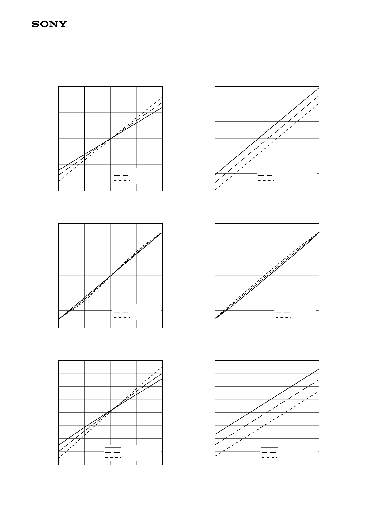
CXA2000Q
Curve Data
I2C bus data conforms to the "I2C Bus Register Initial Settings" of the Electrical Characteristics Measurement
Conditions (P. 22).
4.0
3.5
V-SIZE
3.6
3.4
3.2
V-POSITION
3.0
V [V]
2.5
2.0
0 5 10 15 20
V-SIZE = 0
V-SIZE = 1F
V-SIZE = 3F
Time [ms]
S-CORR
3.6
3.4
3.2
3.0
V [V]
2.8
2.6
2.4
0 5 10 15 20
S-CORR = 0
S-CORR = 7
S-CORR = F
Time [ms]
3.0
V [V]
2.8
2.6
2.4
0 5 10 15 20
V-POSITION = 0
V-POSITION = 1F
V-POSITION = 3F
Time [ms]
V-LIN
3.6
3.4
3.2
3.0
V [V]
2.8
2.6
2.4
0 5 10 15 20
V-LIN = 0
V-LIN = 7
V-LIN = F
Time [ms]
3.8
V-ASPECT
3.6
3.4
3.2
3.0
V [V]
2.8
2.6
2.4
2.2
0 5 10 15 20
V-ASPECT = 0
V-ASPECT = 1F
V-ASPECT = 3F
Time [ms]
– 43 –
3.8
V-SCROLL
3.6
3.4
3.2
3.0
V [V]
2.8
2.6
2.4
2.4
0 5 10 15 20
V-SCROLL = 0
V-SCROLL = 1F
V-SCROLL = 3F
Time [ms]
Page 44
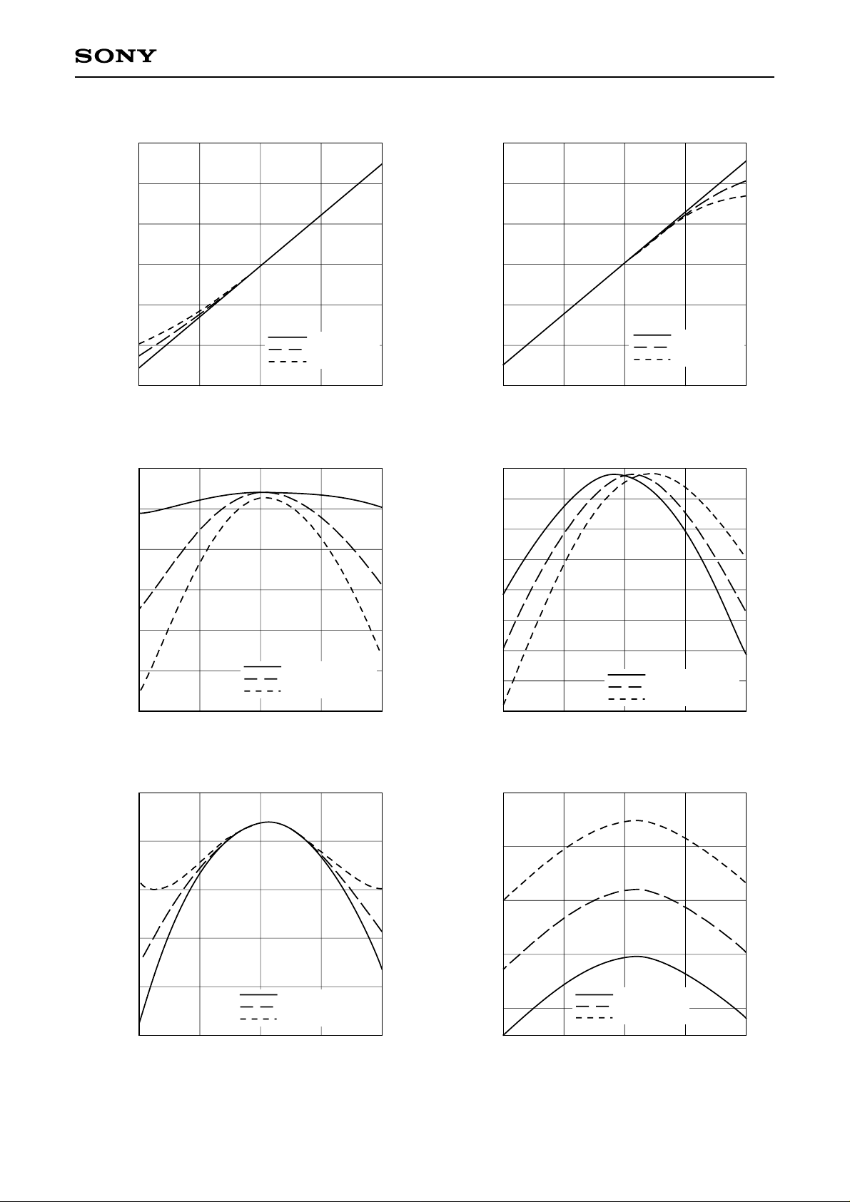
CXA2000Q
UP-VLIN
3.6
3.4
3.2
3.0
V [V]
2.8
2.6
2.4
0 5 10 15 20
UP-VLIN = 0
UP-VLIN = 7
UP-VLIN = F
Time [ms]
PIN-COMP
4.2
4.0
3.8
LO-VLIN
3.6
3.4
3.2
3.0
V [V]
2.8
2.6
2.4
0 5 10 15 20
LO-VLIN = 0
LO-VLIN = 7
LO-VLIN = F
Time [ms]
PIN-PHASE
4.1
4.0
3.9
3.8
3.6
V [V]
3.4
3.2
3.0
0 5 10 15 20
PIN-COMP = 0
PIN-COMP = 1F
PIN-COMP = 3F
Time [ms]
CORNER-PIN
4.2
4.0
3.8
V [V]
3.6
3.4
3.2
0 5 10 15 20
CORNER-PIN = 0
CORNER-PIN = 7
CORNER-PIN = F
Time [ms]
3.7
V [V]
3.6
3.5
3.4
3.3
0 5 10 15 20
PIN-PHASE = 0
PIN-PHASE = 7
PIN-PHASE = F
Time [ms]
H-SIZE
4.8
4.4
4.0
V [V]
3.6
H-SIZE = 0
3.2
0 5 10 15 20
H-SIZE = 1F
H-SIZE = 3F
Time [ms]
– 44 –
Page 45
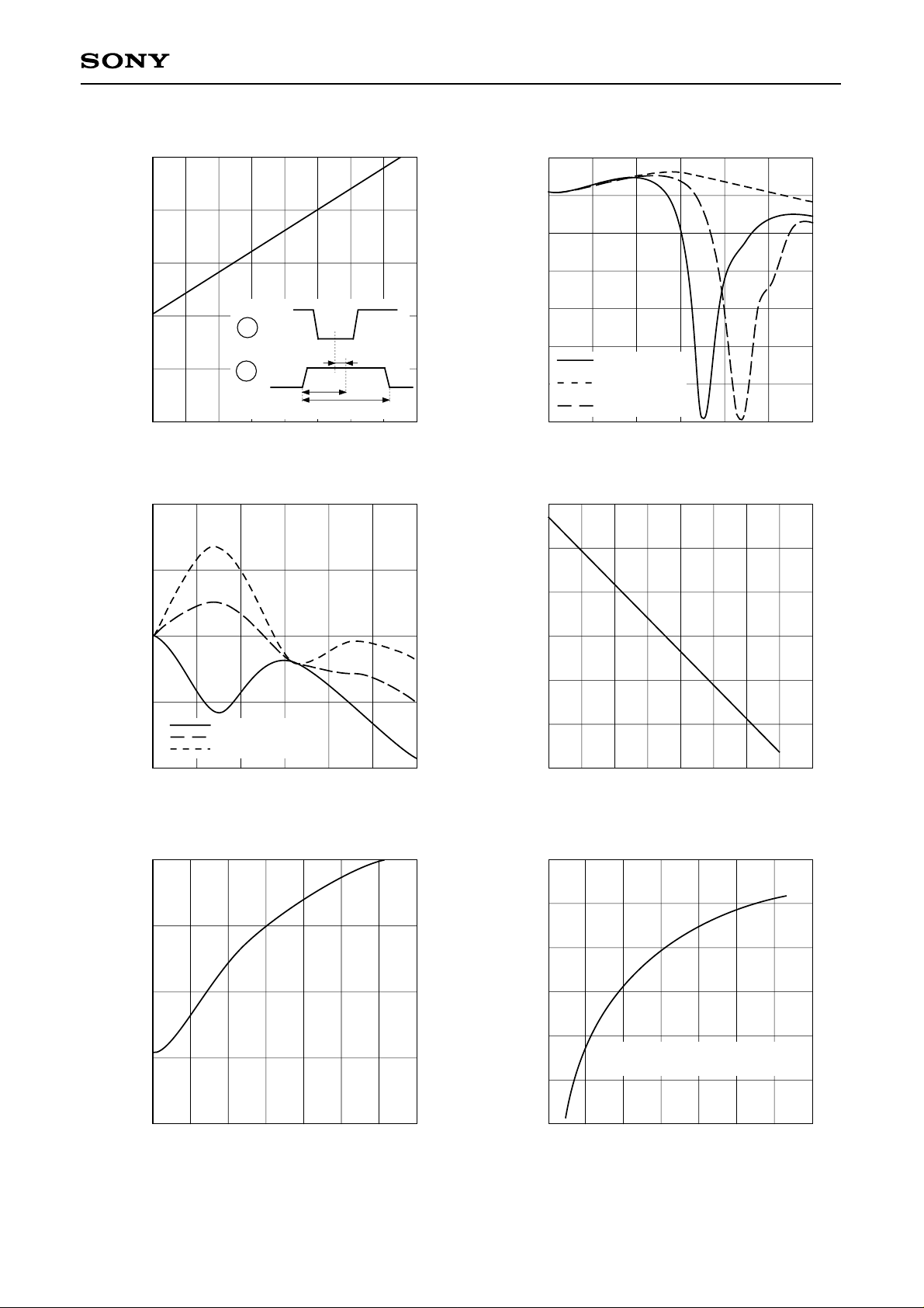
CXA2000Q
H-POSITION
5
4
3
Time [µs]
2
1
0
2 6 10 14
0481216
47
38
HSIN
AFCPIN
DATA
SYNC
center
t [µsec]
6µsec
12µsec
SHARPNESS
10
5
5
0
–5
–10
–15
Gain [dB]
–20
3.58MHz
TRAP OFF = 0
–25
4.43MHz
TRAP OFF = 0
TRAP OFF = 1
–30
135
0246
Frequency [MHz]
DL
800
700
600
TRAP OFF
0
Gain [dB]
–5
SHARPNESS = 0
SHARPNESS = 7
SHARPNESS = F
–10
2610
04812
Frequency [MHz]
PICTURE
0
–5
–10
Gain [dB]
–15
500
400
CVIN – YOUT delay time [ns]
300
200
1357
02468
DATA
COLOR
10
5
0
–5
Gain [dB]
–10
–15
∗
COLOR OFF when DATA = 0
(–40dB or less)
–20
10 30 50
0 20406070
DATA
– 45 –
–20
10 30 50
020406070
DATA
Page 46
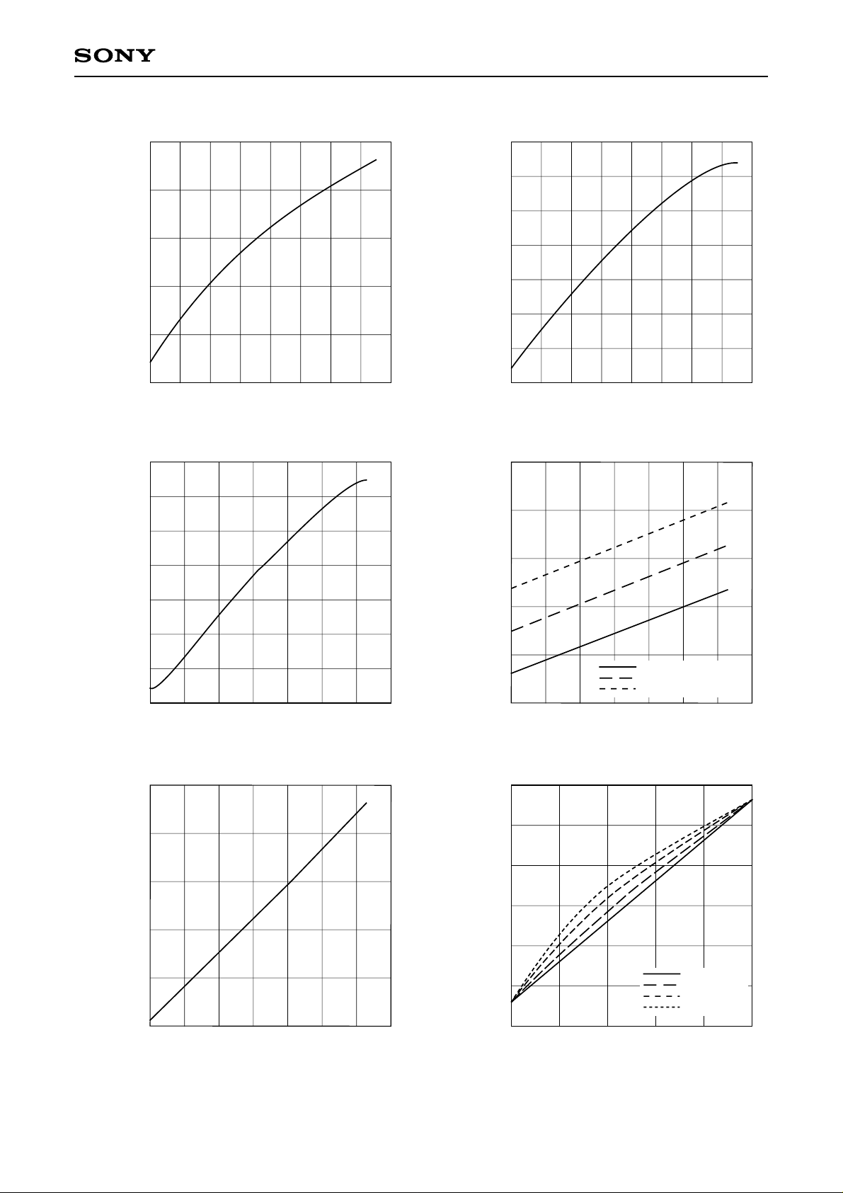
CXA2000Q
SUB-COLOR
4
2
0
Gain [dB]
–2
–4
–6
04812162 6 10 14
DATA
B-DRIVE, G-DRIVE
2
1
0
SUB-CONT
3
2
1
0
–1
Gain [dB]
–2
–3
–4
2 6 10 14
04812
DATA
BRIGHT
1
0.5
16
–1
–2
Gain [dB]
–3
–4
–5
0 2040607010 30 50
SUB-BRIGHT
0.2
0
–0.2
–0.4
DATA
0
–0.5
–1.0
–1.5
and black level [Vp-p]
Potential difference between Rch reference pulse level
10 30 50
020406070
SUB-BRIGHT = 0
SUB-BRIGHT = 1F
SUB-BRIGHT = 3F
DATA
GAMMA
4.5
4.0
3.5
3.0
Rch output [V]
2.5
–0.6
–0.8
and black level [Vp-p]
Potential difference between Rch reference pulse level
10 30 50
0 20406070
DATA
– 46 –
2.0
1.5
0 20 40 80 100
CVIN input amplitude [IRE]
GAMMA = 0
GAMMA = 1
GAMMA = 2
GAMMA = 3
60
Page 47
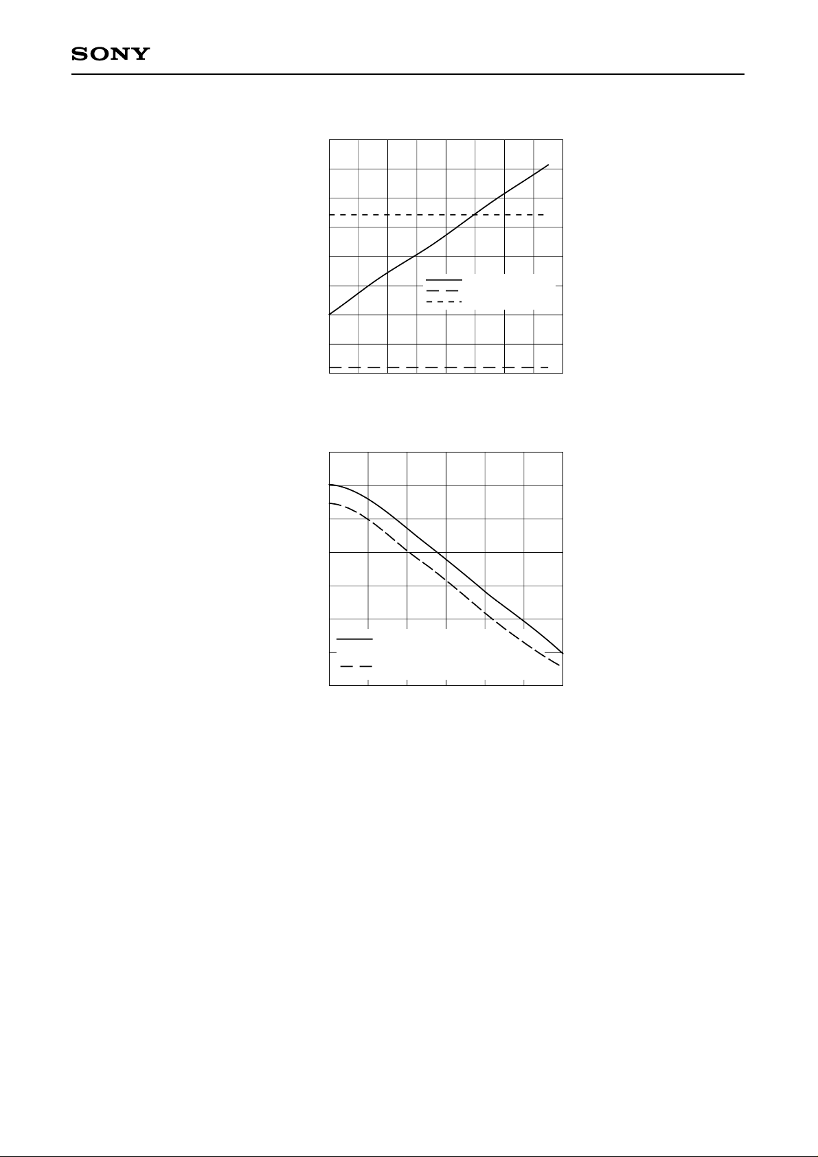
G-CUTOFF, B-CUTOFF
4.2
4.0
3.8
3.6
3.4
3.2
3.0
IKIN reference pulse voltage [V]
2.8
Gch, Bch
IK clamp level
Rch
CXA2000Q
2.6
2
04 16
612
81410
DATA
AKB open loop characteristics
3.5
3.0
2.5
2.0
V [V]
1.5
1.0
Reference pulse voltage
(AKBOFF = 0)
0.5
RGBOUT black level voltage
(AKBOFF = 0, 1)
0
Voltage applied to R, G and B sample-and-hold capacitance pins [V]
3.5 4.0 5.0
3.0 6.0
5.54.5
– 47 –
Page 48
Package Outline Unit: mm
CXA2000Q
64PIN QFP (PLASTIC)
52
64
SONY CODE
EIAJ CODE
JEDEC CODE
51
1
1.0
QFP-64P-L01
∗QFP064-P-1420-A
23.9 ± 0.4
+ 0.4
20.0 – 0.1
+ 0.15
0.4 – 0.1
33
32
+ 0.4
14.0 – 0.1
17.9 ± 0.4
20
19
+ 0.35
2.75 – 0.15
M
± 0.12
PACKAGE STRUCTURE
PACKAGE MATERIAL
LEAD TREATMENT
LEAD MATERIAL
PACKAGE WEIGHT
EPOXY / PHENOL RESIN
SOLDER PLATING
42 ALLOY
1.5g
+ 0.1
0.15 – 0.05
0.15
+ 0.2
0.1 – 0.05
16.3
0.8 ± 0.2
– 48 –
 Loading...