

Page 1
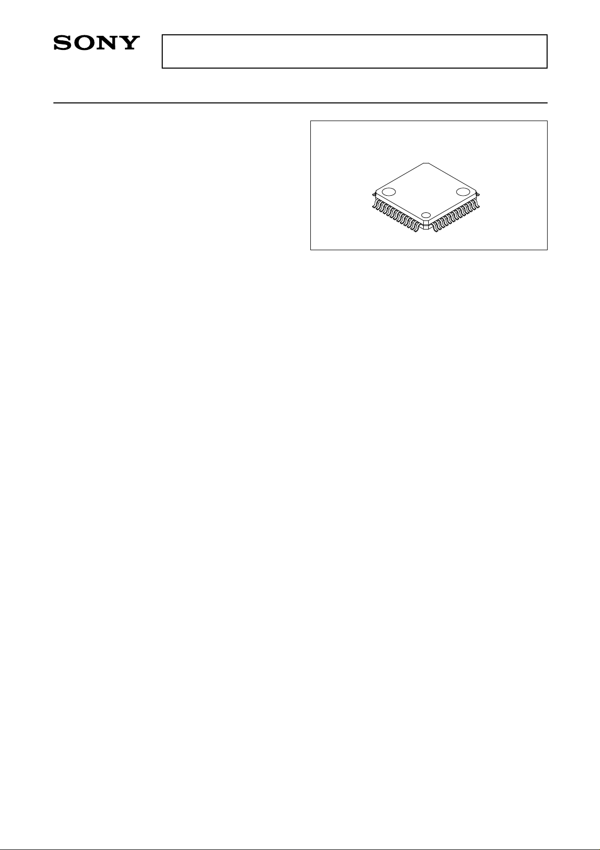
CXA1992R
For the availability of this product, please contact the sales office.
RF Signal Processing Servo Amplifier
Description
The CXA1992R is a bipolar IC developed for CD
player RF signal processing and servo control. This
IC supports three-spot optical system pickups.
Features
• Automatic focus bias adjustment circuit
• Automatic tracking balance and gain adjustment
circuits
• RF level control circuit
• Interruption countermeasure circuit
• Sled overrun prevention circuit
• Anti-shock circuit
• Defect detection and prevention circuits
• RF 1-V amplifier, RF amplifier
• APC circuit
• Focus and tracking error amplifier
• Focus, tracking and sled servo control circuits
• Focus OK circuit
• Mirror detection circuit
• Single power supply and dual power supplies
Absolute Maximum Ratings (Ta = 25°C)
• Supply voltage VCC 12 V
• Operating temperature Topr –20 to +75 °C
• Storage temperature Tstg –65 to +150 °C
• Allowable power dissipation
Recommended Operating Conditions
Operating supply voltage VCC – VEE 3.0 to 5.5 V
Preliminary
52 pin LQFP (Plastic)
PD 600 mW
Applications
CD players
Structure
Bipolar silicon monolithic IC
Sony reserves the right to change products and specifications without prior notice. This information does not convey any license by
any implication or otherwise under any patents or other right. Application circuits shown, if any, are typical examples illustrating the
operation of the devices. Sony cannot assume responsibility for any problems arising out of the use of these circuits.
– 1 –
PE96527-ST
Page 2

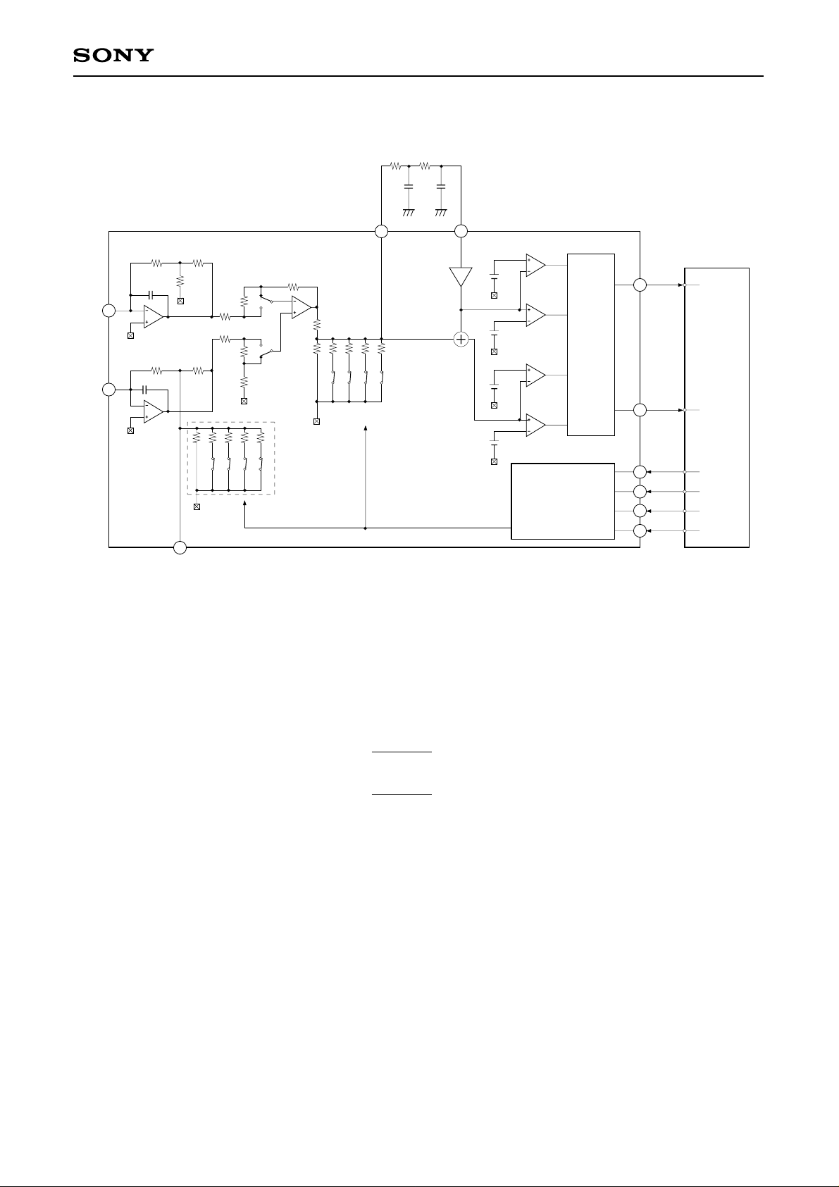
Block Diagram
CXA1992R
FE_BIAS
ATSC
TDFCT
8
RF_I
VEE
MIRR
TGFL
VCC
Charge
VEE
SRCH
CP
31
VCC
VEE
IIL DATA REGISTER
INPUT SHIFT REGISTER
ADDRESS DECODER
SENS SELECTOR
OUTPUT DECODER
BAL1-4
TOG1-4
up
9
TGU
CB
CC1
29
DFCT1
FSET
11
28
CC1
PS1-4TM1-7TG1-2FS1-4IFB1-6
12
FSET
30
VCC
DFCT
IIL
↓
TTL
MIRR
TM7
TG2
10
TG2
CC2
TA_M
FOK
27
SENS2
26
IIL
↓
TTL
TTL
↓
IIL
VCC
ISET
VCC
VCC
TM6
TM4
TM5
TM3
VEE
VEE
13
TA_O
SENS1
25
C. OUT
24
XRST
23
DATA
22
XLT
21
CLK
20
19
LOCK
18
CC
V
ISET
17
16
SL_O
15
SL_M
14
SL_P
TM2
PD
VEE
LASER POWER CONTROL
IFB3
IFB4
TRK. GAIN
WINDOW COMP.
TG1
DFCT
FS4
3
FDFCT
LD
35
36
VEE
FE AMP
IFB5
IFB6
TRACKING
PHASE COMPENSATION
FOCUS
PHASE COMPENSATION
4
FGD
PD2
PD1
37
38
39
PD1 IV
PD2 IV
AMP
AMP
40
41
F
E
42
43
EI
V
EE
44
TEO
45
46
LPFI
47
TEI
48
49
TZC
50
51
VC
52
FZC
V
EE
E IV AMP
TOG2
TOG1
TZC COMP.
VCC
FZC COMP.
F IV AMP
BAL2
BAL1
TOG4
TOG3
ATSC
WINDOW
COMP.
VCC
BAL3
VEE
BAL4
1
FEO
TGFL
E-F BALANCE
WINDOW COMP.
DFCT
TM1
2
FEI
VCC
APC
VCC
IFB2
IFB1
VEE
RFTC
FO. BIAS
WINDOW COMP.
5
FLB
RF_M
34
RF SUMMING AMP
FOH
FOL
TGH
TGL
BALH
BALL
ATSC
TZC
FZC
6
FE_O
RF_O
32
33
VEE
LEVEL S
VCC
FOK
LDON
LPC
LPCL
DFCTO
FS1
FS2
7
FE_M
– 2 –
Page 3

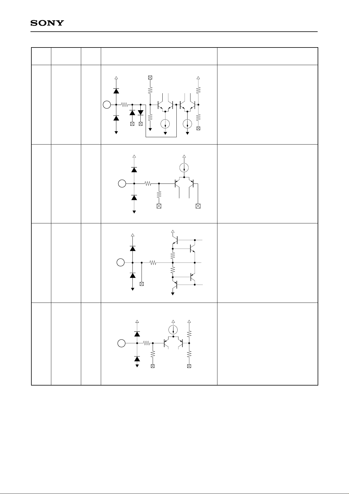
Pin Description
CXA1992R
Pin
No.
1
2
3
Symbol
FEO
FEI
FDFCT
I/O
O
I
I
Equivalent circuit
25p
147
1
174k
300µ
147
2
100k
147
3
10µ
10µ
3µ
Focus error amplifier output.
Connected internally to the window
comparator input for bias
adjustment.
Focus error input.
Capacitor connection pin for defect
Description
time constant.
4
5
6
13
16
FGD
FLB
FE_O
TA_O
SL_O
Ground this pin through a capacitor
for cutting the focus servo highfrequency gain.
External time constant setting pin
for boosting the focus servo lowfrequency.
Focus drive output.
Tracking drive output.
Sled drive output.
40k
68k
130k
4µ
330k
470k
I
147
4
5
I
O
6
O
O
13
16
250µ
FE_M
7
I
7
147
90k
Focus amplifier inverted input.
50k
2µ
– 3 –
Page 4

CXA1992R
Pin
No.
8
9
10
Symbol
SRCH
TGU
TG2
I/O
I
I
I
Equivalent circuit
147
8
50k
110k
20k
9
147
11µ
External time constant setting pin for
generating focus search waveform.
External time constant setting pin
for switching tracking high-
Description
frequency gain.
82k
External time constant setting pin for
10
470k
switching tracking high-frequency
gain.
11
12
14
FSET
TA_M
SL_P
I
11
147k
Peak frequency setting pin for focus
and tracking phase compensation
amplifier.
15k 15k
147
100k
Tracking amplifier inverted input.
11µ
Sled amplifier non-inverted input.
2µ
I
I
12
14
147
15
SL_M
I
15
147
22µ
Sled amplifier inverted input.
– 4 –
Page 5

CXA1992R
Pin
No.
17
Symbol
ISET
18 VCC
19 LOCK
CLK
20
22
DATA
I/O
I
I
Equivalent circuit
Description
Connect an external capacitance to
17
147
set the current which determines
the Focus search, Track jump, and
Sled kick heights.
50µ
V
18
CC
Positive power supply.
The sled overrun prevention circuit
I
19
I
20
22
147
1k
20µ
I
operates when this pin is Low.
(no pull-up resistance)
Serial data transfer clock input from
CPU. (no pull-up resistance)
Serial data input from CPU.
(no pull-up resistance)
21
23
24
25
26
27
XLT
XRST
C. OUT
SENS1
SENS2
FOK
I
147
21
23
I
2k
5p
20µ
O
O
24
25
26
147
O
20k
100k
Latch input from CPU.
(no pull-up resistance)
Reset input; resets at Low.
(no pull-up resistance)
Track number count signal output.
Outputs FZC, DFCT1, TZC, BALH,
TGH, FOH, ATSC, and others
according to the command from CPU.
Outputs DFCT2, MIRR, BALL, TGL,
FOL, and others according to the
command from the CPU.
20k
O
27
147
40k
Focus OK comparator output.
– 5 –
100k
Page 6
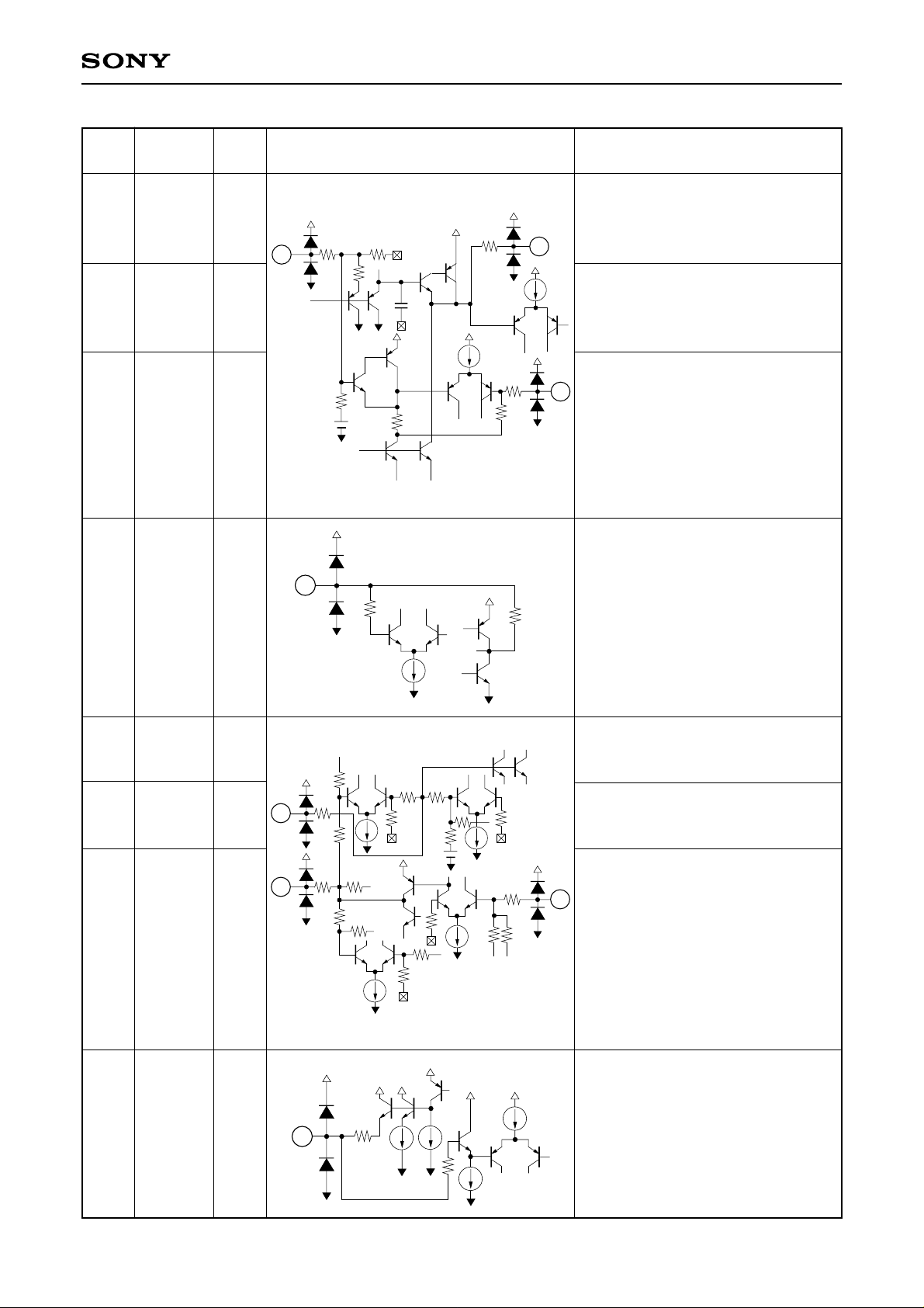
CXA1992R
Pin
No.
28
29
30
31
Symbol
CC2
CC1
CB
CP
I/O
I
O
I
I
30
31
120k
Equivalent circuit
147
11k
100k
147
147
43k
29
1.5k
Description
Input for the defect bottom hold
output with capacitance coupled.
Defect bottom hold output.
Connected internally to the
interruption comparator input.
28
Connection pin for defect bottom
hold capacitor.
Connection pin for MIRR hold
capacitor.
MIRR comparator non-inverted
input.
RF_I
32
33
RF_O O
34
RF_M
RFTC
35
I
147
32
147
33
147
Input for the RF summing amplifier
output with capacitance coupled.
RF sunning amplifier output. Eyepattern check point.
34
RF summing amplifier inverted
10k10k
I
input.
The RF amplifier gain is determined
by the resistance connected
between this pin and RFO pin.
I
35
147
50µ
50µ
External time constant setting pin
during RF level control.
10µ
– 6 –
Page 7
CXA1992R
Pin
No.
36
37
Symbol
LD
PD
I/O
O
I
37
Equivalent circuit
36
8µ
147
1k
10k
20µ
55k
10k
Description
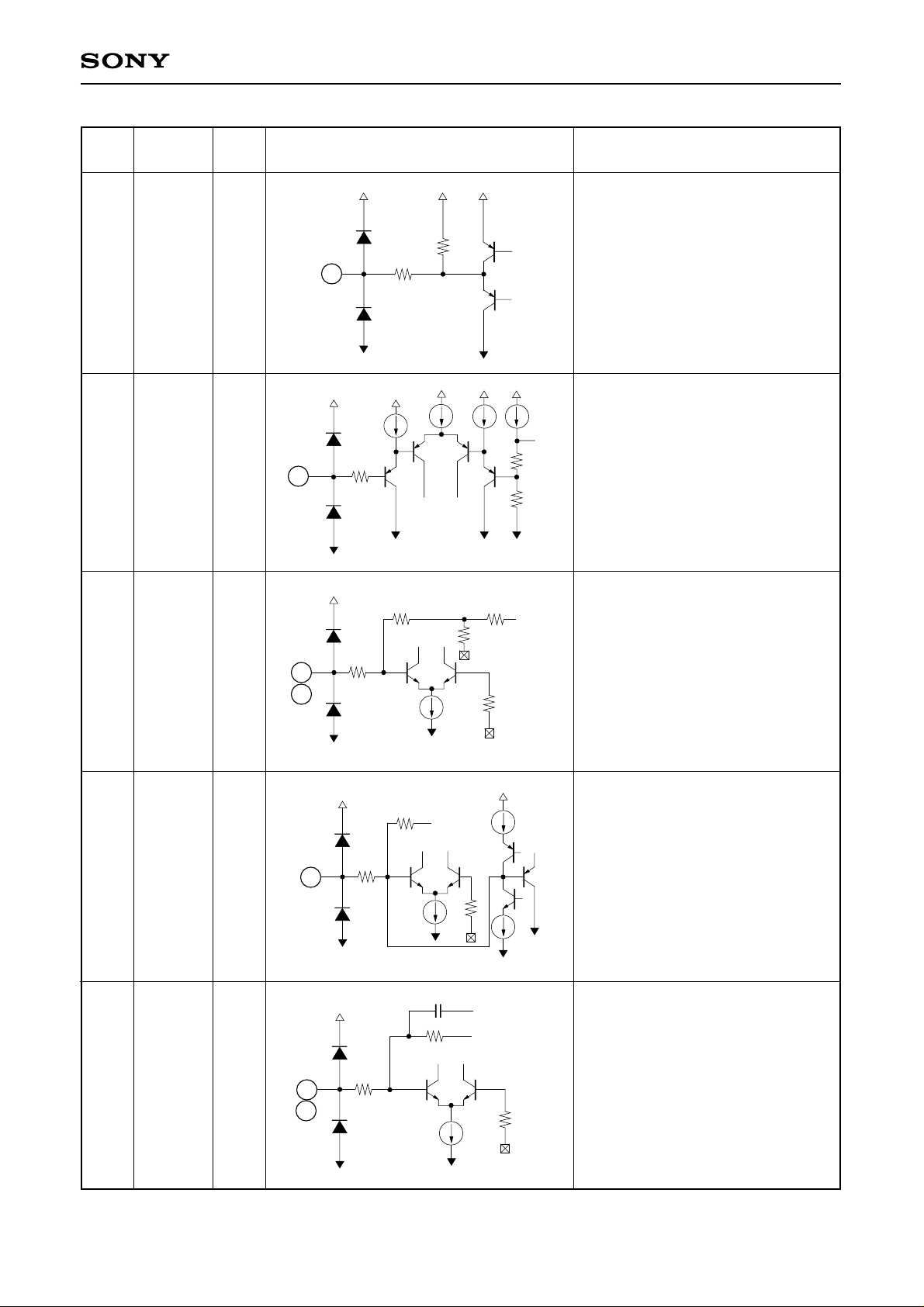
APC amplifier output.
APC amplifier input.
38
39
40
41
42
PD1
PD2
FE_BIAS
F
E
10k
I
I
38
39
147
4k
100µ
8k
2k
RF I-V amplifier inverted input.
Connect these pins to the photo
diode A + C and B + D pins.
11.6k
Bias adjustment of focus error
I
40
I
I
41
42
147
6µ
12p
260k
147
500
10µ
amplifier.
Leave this pin open for automatic
adjustment.
F I-V and E I-V amplifier inverted
input.
Connect these pins to photo diodes
F and E.
– 7 –
Page 8
CXA1992R
Pin
No.
43
44
45
Symbol
EI
VEE
TEO
I/O
—
—
O
45
43
Equivalent circuit
6.8k
260k
147
44
147
16k 7.5k 1.5k7.5k
10k
110k 56k 13k
75k
150k
27k
VEE
3.3k
150k
Description
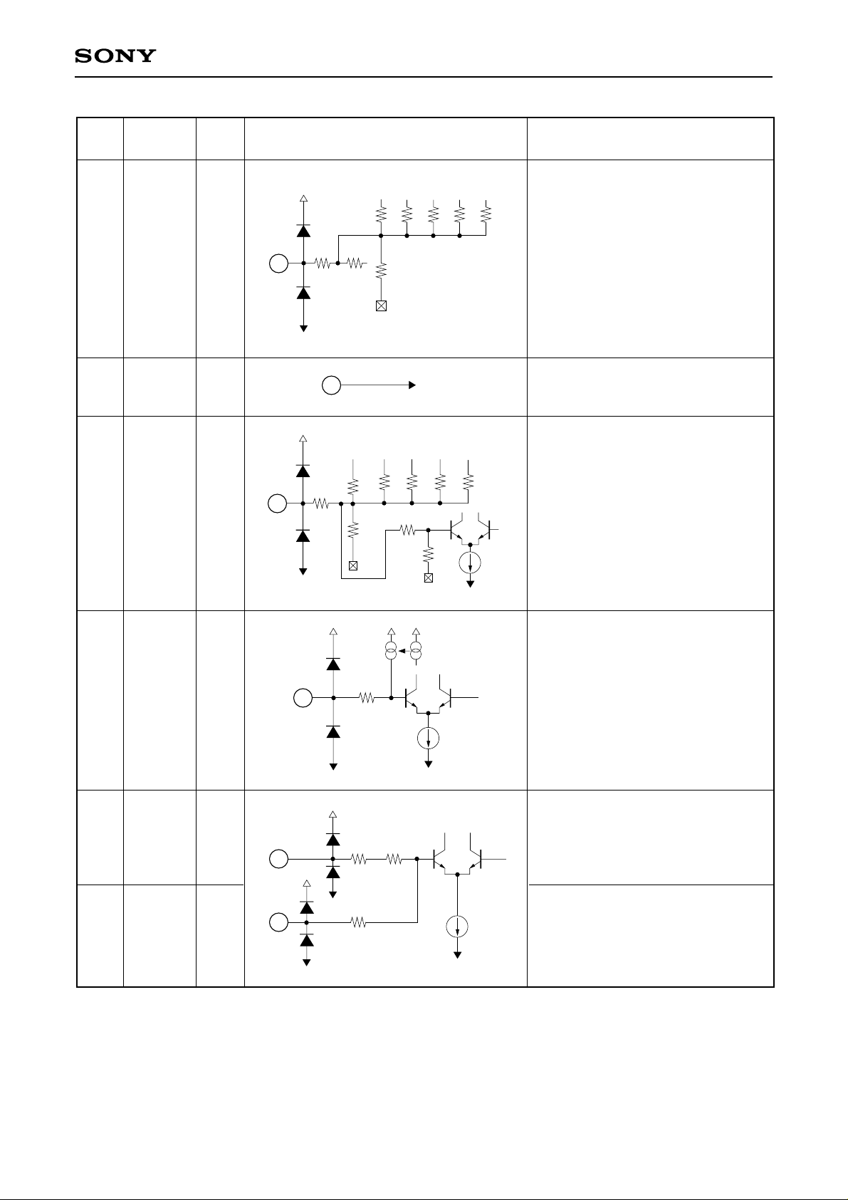
I-V amplifier E gain adjustment.
(When not using automatic balance
adjustment)
Negative power supply.
Tracking error amplifier output.
E-F signal is output.
46
47
50
LPFI
TEI
TDFCT
I
46
147
Comparator input for balance
adjustment.
(Input from TEO through LPF)
7µ
I
47
I
50
147
147
100k
3µ
Tracking error input.
Capacitor connection pin for defect
time constant.
– 8 –
Page 9
CXA1992R
Pin
No.
48
49
Symbol
ATSC
TZC
I/O
I
I
48
Equivalent circuit
147
49
1k
100k
10µ 10µ
147
Description
100k
Window comparator input for ATSC
detection.
1k
10µ
Tracking zero-cross comparator
input.
75k
51
52
VC
FZC
10µ
120
(VCC + VEE)/2 direct voltage output.
120
51k
Focus zero-cross comparator input.
O
I
51
52
50
VC
147
75k 9k
– 9 –
Page 10

CXA1992R
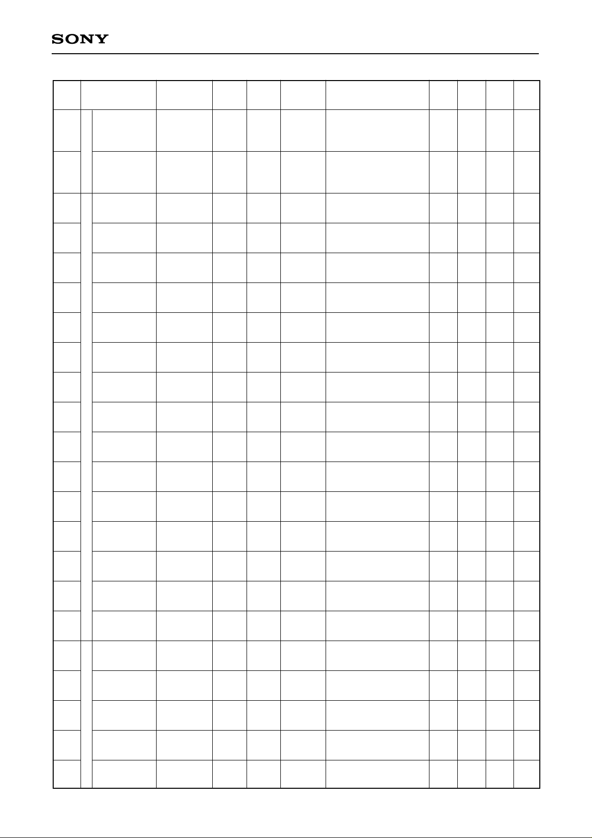
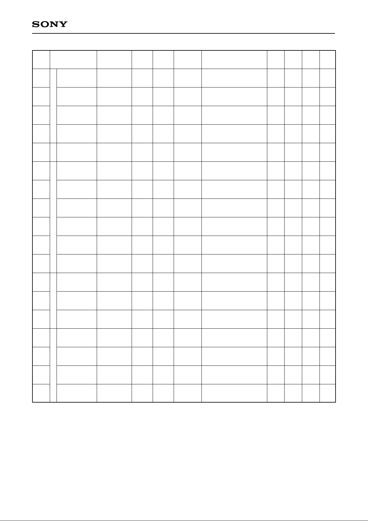
Electrical Characteristics (VCC = 1.5V, VEE = 1.5V, Topr = 25°C)
TEST
T1
T2
T3
T4
T5
T6
T7
T8
T9
Item
Current
consumption 1
Current
consumption 2
Center amplifier
output offset
Offset
Voltage gain
RF amplifier
Max. output
amplitude - High
Max. output
amplitude - Low
Offset
Voltage gain 1
(PHD1)
SW conditions
(ON switches)
51
51
51, 51D
33S, 38, 39
33D, 38
33D, 39
1D
1S, 38
SD
RST
RST
RST
RST
RST
RST
RST
39F
39F
Input
pin
18
44
—
38
39
38
39
38
39
38
Measurement pin
18
44
51
33
33
33
33
1
1
Measurement
conditions
1kHz I/O ratio
V2 = 0.2VDC
V2 = 0.2VDC
1FB6: ON
1kHz I/O ratio
Min. Typ. Max. Unit
mA
31.2
24.0
16.8
100
50
31.1
—
–0.3
120
33
mA
mV
mV
dB
mV
dB
–31.2
–100
–50
25.1
1.2
—
–120
27
–24.0
0
0
28.1
0
30
–16.8
V
V
T10
T11
T12
T13
T14
T15
T16
T17
T18
T19
Voltage gain 2
(PHD2)
Voltage gain
difference
Max. output
voltage – High
Max. output
voltage – Low
BIAS0
FE amplifier
BIAS1
BIAS2
BIAS3
BIAS4
BIAS5
1S, 39
1S
1D, 39
1D, 38
1D
1D
1D
1D
1D
1D
39F
39F
39F
39F
3BF
3BE
3BD
3BB
3B7
3AF
39
39
38
1
1
1
1
1
1
1
1
1
1kHz I/O ratio
V2 = 100mVDC
V2 = 100mVDC
IFB1, 2, 3, 4, 5, 6:
OFF
IFB1: ON, BIAS0:
reference
IFB2: ON, BIAS0: reference
Output gain difference with T15
IFB3: ON, BIAS0: reference
Output gain difference with V17
IFB4: ON, BIAS0: reference
Output gain difference with V18
IFB5: ON, BIAS0: reference
Output gain difference with V19
27
–3
1
—
560
30
0
1.3
–1.3
801
–25
6
6
6
6
33
3
—
–1
1042
dB
dB
V
V
mV
mV
dB
dB
dB
dB
T20
BIAS6
1D
39F
1
– 10 –
IFB6: ON, BIAS0: reference
Output gain difference with V20
6
dB
Page 11
CXA1992R
TEST Item
T21
T22
T23
T24
T25
T26
T27
T28
FOH threshold
FOL threshold
FE amplifierTE amplifierAPC
Offset
GAIN UP (F)
GAIN UP (E)
Voltage gain
F0
Voltage gain
F1
Voltage gain
F2
SW conditions
(ON switches)
1D, 25D, 40
1D, 26D, 40
45D
41, 45S
42, 45S
41, 45S
41, 45S
41, 45S
SD
39F
39F
34F
308
36F
308
36F
308
34F
34E
30F
34D
Input
pin
40
40
41
42
41
42
41
41
41
Measurement pin
1
1
45
45
45
45
45
45
Measurement
conditions
I
FB6: ON
Pin 1 voltage when SENS1
(Pin 25) goes from High to Low
IFB6: ON
Pin 1 voltage when SENS2
(Pin 26) goes from High to Low
TOG: OFF,
BAL1, 2, 3: ON
V1 = 2 kHz, I/O ratio
TOG: OFF, BAL1, 2, 3: ON
V1 = 2 kHz, I/O ratio
TOG: OFF, BAL1, 2, 3: ON
V1 = 2kHz, TOG: OFF
I/O ratio
V1 = 2kHz, TOG1: ON
Reference to F0
V1 = 2kHz, TOG2: ON
Reference to F0
Min. Typ. Max. Unit
–25
8.6
8.6
2.5
–2.6
–4.4
20
–20
0
11.6
11.6
5.5
–2.1
–3.9
25
14.6
14.6
8.5
–1.6
–3.4
mV
mV
mV
dB
dB
dB
dB
dB
T29
T30
T31
T32
T33
T34
T35
T36
T37
T38
Voltage gain
F3
Voltage gain
F4
Voltage gain
E0
Voltage gain
E1
Voltage gain
E2
Voltage gain
E3
Voltage gain
E4
Max. output
voltage – High
Max. output
voltage – Low
Output voltage
1
41, 45S
41, 45S
42, 45S
42, 45S
42, 45S
42, 45S
42, 45S
41, 45D
42, 45D
36D, 37
34B
347
34F
30F
00
30E
30D
30B
307
34F
308
34F
308
3C4
41
41
42
42
42
42
42
41
42
37
45
45
45
45
45
45
45
45
45
36
V1 = 2kHz, TOG3: ON
Reference to F0
V1 = 2kHz, TOG4: ON
Reference to F0
V1 = 2kHz, BAL: OFF
I/O ratio
V1 = 2kHz, BAL1: ON
Reference to E0
V1 = 2kHz, BAL2: ON
Reference to E0
V1 = 2kHz, BAL3: ON
Reference to E0
V1 = 2kHz, BAL4: ON
Reference to E0
V1 = 1VDC, TOG: OFF,
BAL1, 2, 3: ON
V1 = 1VDC, TOG: OFF,
BAL1, 2, 3: ON
I37 = 364µA
–7.7
–12.2
–0.33
0.17
0.6
1.46
3.03
0.5
—
–7.2
–11.7
2.67
0.47
0.9
1.76
3.33
–704
–6.7
–11.2
5.67
0.77
1.2
2.06
3.63
—
–0.5
dB
dB
dB
dB
dB
dB
dB
V
V
mV
T39
T40
T41
T42
Output voltage
2
Output voltage
3
Output voltage
4
LD OFF
36D, 37
36D, 37
36, 36D
36, 36D, 37
3C4
3C4
3C4
3C0
37
37
37
37
36
36
36
36
– 11 –
I37 = 439µA
I37 = 515µA
0.8mA sink
I37 = 515µA,
LD: OFF
0
1.1
–233
669
1.3
500
—
mV
mV
mV
V
Page 12

CXA1992R
TEST Item
T43
T44
T45
T46
T47
T48
T49
T50
T51
30% limit
10% limit
RF AGC
–30% limit
–10% limit
Direct voltage
gain
FCS total gain
Feed through
1
FZC threshold
Max. output
voltage – High
Focus servo
SW conditions
(ON switches)
32, 36D, 37
32, 36D, 37
36D, 37, 38,
39
36D, 37, 38,
39
2, 6D
2, 6S
26D, 52
2, 6D, 6S
SD
3C7
3C5
3C7
3C5
08
—
00
08
00
08
Input
pin
37
32
37
32
37
38
39
37
38
39
2
—
2
52
2
Measurement pin
36
36
36
36
6
—
6
52
6
Measurement
conditions
I37 = 439µA
Output difference with T39
I37 = 439µA
Output difference with T39
I37 = 515µA
Output difference with T40
I37 = 515µA
Output difference with T40
T9 + T47
Output gain difference between
SD = 00 and SD = 08.
Pin 52 voltage when SENS1
(Pin 25) goes from Low to High
V1 = 200mVDC
Min. Typ. Max. Unit
18
49
—
181
1
1304
470
–1307
–466
21
51
—
221
1.3
24
53
–30
261
—
mV
mV
mV
mV
dB
dB
dB
mV
V
T52
T53
T54
T55
T56
T57
T58
T59
T60
T61
T62
T63
T64
Max. output
voltage – Low
Search
voltage (–)
Search
voltage (+)
Direct voltage
gain
TRK total gain
Feed through
1
Max. output
voltage – High
Max. output
voltage – Low
Jump output
voltage (–)
Tracking servo
Jump output
voltage (+)
ATSC
threshold (–)
ATSC
threshold (+)
TZC threshold
2, 6D, 6S
6D
6D
13D, 47
13S, 47
13D, 47
13D, 47
13D
13D
10, 10D, 48
10, 10D, 48
25D, 49,
49B
08
02
03
25
—
20
25
20
25
20
25
2C
28
10
10
20
—
—
47
—
47
47
47
48
48
49
V1 = –200mVDC
2
6
6
6
13
—
13
13
13
T26 + T55
Output gain difference between
SD = 20 and SD = 25.
V1 = –0.5VDC
V1 = 0.5VDC
13
13
48
48
49
Input voltage when TG2
(Pin 10) goes from Vcc/2 to Vcc
Input voltage when TG2 (Pin 10)
goes from Vcc/2 to Vcc
Pin 49 voltage when
SENS1 (Pin 25) is 0V
—
–640
360
12.2
18.1
—
1
—
–640
360
–25
7
–20
–1.3
–500
500
14.6
20.1
—
1.3
–1.3
–500
500
–15
15
0
–360
640
17.6
22.1
–39
–360
640
–1
—
–1
–7
25
20
V
mV
mV
dB
dB
dB
V
V
mV
mV
mV
mV
mV
– 12 –
Page 13
CXA1992R
TEST Item
T65
T65
T67
T68
T69
T70
T71
T72
T73
BAL COMP
threshold – High
BAL COMP
threshold – Low
GAIN COMP
threshold – High
Tracking servoFOKSled servo
GAIN COMP
threshold – Low
FOK
threshold
Voltage gain
Feed through
Max. output
voltage – High
Max. output
voltage – Low
SW conditions
(ON switches)
25D, 46,
46B
26D, 46,
46B
25D, 45,
45D
26D, 45,
45D
27D, 32
14, 14B, 15,
16S
14, 14B,
16S
14, 14B,
16D
14, 14B,
16D
SD
300
300
340
340
—
25
20
25
25
25
Input
pin
46
46
45
45
32
14
14
14
14
Measurement pin
46
46
45
45
32
16
16
16
16
Measurement
conditions
Pin 46 voltage when SENS1
(Pin 25) goes from High to Low
Pin 46 voltage when SENS2
(Pin 26) goes from High to Low
Pin 45 voltage when SENS1
(Pin 25) goes from High to Low
Pin 45 voltage when SENS2
(Pin 26) goes from Low to High
Pin 32 voltage when
Pin 27 is 0V
V1 = 100 Hz, I/O ratio
Output gain difference between
SD = 20 and SD = 25.
V1 = 400mVDC
V1 = 400mVDC
Min. Typ. Max. Unit
50
—
1
—
20
–20
400
300
–367
—
—
1.3
–1.3
—
–34
—
–1
mV
mV
mV
mV
mV
dB
dB
V
V
T74
T75
T76
T77
T78
T79
T80
T81
T82
Kick voltage 1
Kick voltage 2
Max. operating
frequency 1
Min. input
operating voltage 1
MIRROR
Max. input
operating voltage 1
Min. operating
frequency 1
Max. operating
frequency 1
Min. input
DEFECT
operating voltage 1
Max. input
operating voltage 1
16D
16D
26S, 32
26S, 32
26S, 32
25S, 38, 39
25S, 38, 39
25S, 38, 39
25S, 38, 39
20
20
20
20
20
10
10
10
10
—
—
32
32
32
38
39
38
39
38
39
38
39
16
16
26
26
26
25
25
25
25
REV × 1
FWD × 1
Measures at SENS2
pin.
Measures at SENS2
pin.
Measures at SENS2
pin.
Measures at SENS1
pin.
Measures at SENS1
pin.
Measures at SENS1
pin.
Measures at SENS1
pin.
–750
450
30
—
1.8
—
2.5
—
1.8
–600
600
—
—
—
—
—
—
—
–450
750
—
0.3
—
1
—
0.5
—
mV
mV
kHz
Vp-p
Vp-p
kHz
kHz
Vp-p
Vp-p
– 13 –
Page 14
CXA1992R
DC OUTPUT
GND
GND
STORAGE2
R21
R18
GND
100
10k
I36
I37
R35
R31
0mA
0mA
R24
GNDGND
10k
100k
XRST
DATA
XLT
CLK
20
CLK
LPFI
46
D_GND
C10 33µ
S19
19
LOCK
TEI
47
R43 120k
S17
18
CC
V
ATSC
48
10k
R50
100
R49
C11 47µ
A18
17
TZC
49
ISET
S16D
R37
S16S
120k
R42
16
SL_O
TDFCT
50
R41
R36
R44
13k
5.1k
S15
A14
S16
10k
60k
15
SL_M
VC
51
14
SL_P
FZC
52
S14B
S14
13k
S10
1000P
R13
R33
R30
R27
S10D
R23
47k
C3
200k
100k
10k
200k
1000P
R34
S13S
S6S
R16
R8
100
R32
S13D
10k
R29
10k
R26
10k
R25
S8D
S6D
10k
R22
100
R19
13k
A3
100
R10
R7
10k
10k
TA_O
TA_M
FSET
TG2
TGU
SRCH
FE_M
FE_O
FLB
FGD
FDFCT
FEI
FEO
13
S12
121
C8
0.01µ
11
R28
510k
10
S9
9
8
S7
7
R20
100k
6
C4
5
S5
4
S4
S3
3
S2
2
S1S
S1D
STORAGE1
GND
GND
100
100
R47
S26D
RF_O
RF_M
RFTC
R52
10k
10k
R40
26
SENS2
FE_BIAS
40
S25S
R46
S25D
R51
10k
R39
25
SENS1
F
41
100
10k
S24S
R45
S24D
10k
10k
R38
24
C. OUT
E
42
23
XRST
EI
43
22
DATA
EE
V
44
21
XLT
TEO
45
100
R54
C9
S28
3300p
C7
1000p
C6
3300p
10k
S33S
C5
S33D
1M
R15
10k
R14
330
R12
10k
R11
R9
10k
S27S
0.1µ
S37
S38
S39
S32
S27D
R17
S36D
S36
R53
S26S
10k
R48
FOK
2728
CC2
CC1
29
CB
30
CP
31
RF_I
32
33
22k
34
35
LD
36
PD
37
PD1
38
PD2
39
AC
DC
V2
EE
GND
V
VCC
S40
S41
S42
S43
I40
0mA
R5
390k
R4
R6
390k
S45
13k
C2 33µ
A44
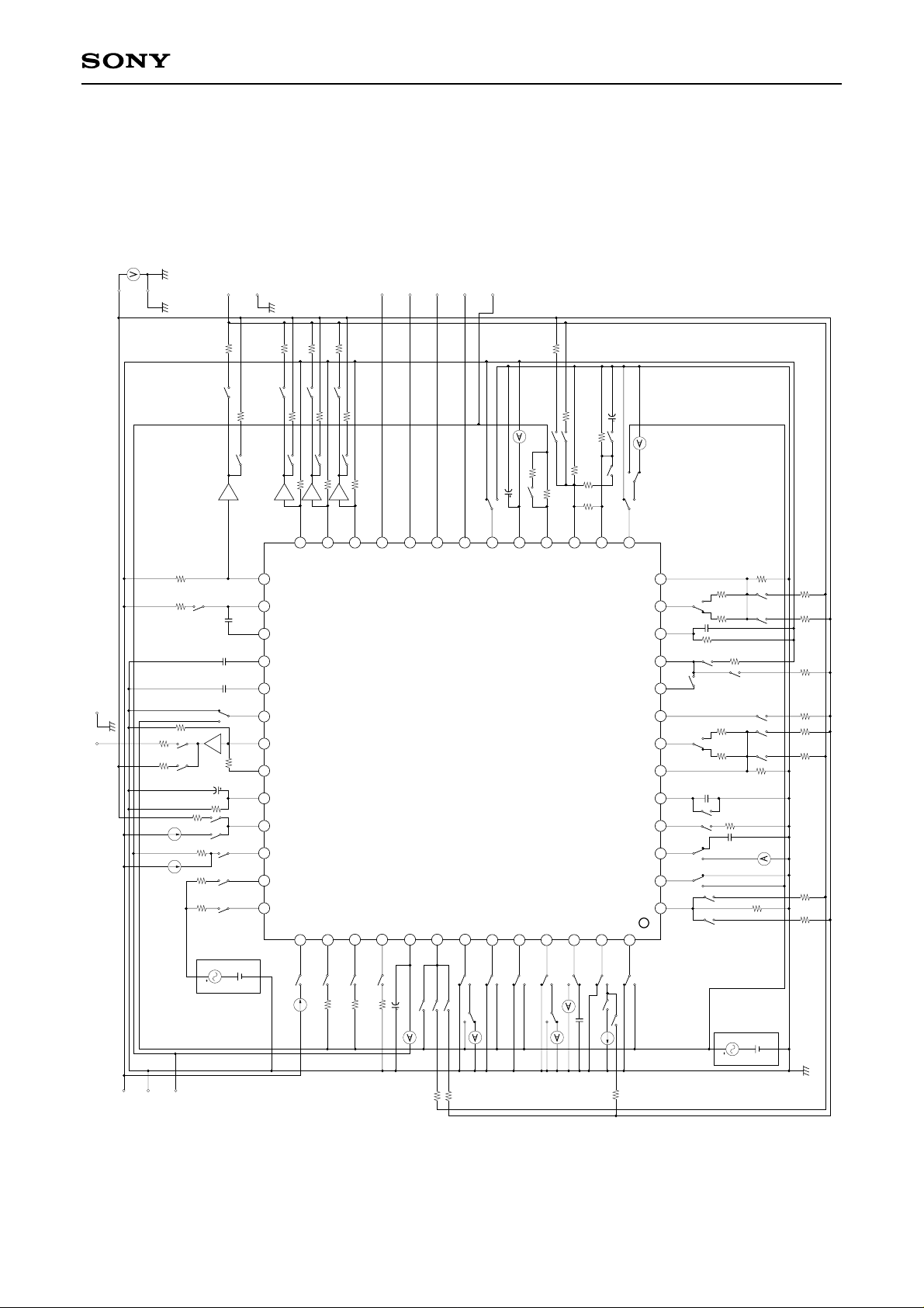
Electrical Characteristics Measurement Circuit
S45S
R2
100
S46
S45D
S46B
R1
10k
– 14 –
S47
S48
A46
S50
S49
A50
S49B
A49
C1
1000P
S52
S51
S51I
I51
S51D
R3
0mA
10k
AC
DC
V1
GND
Page 15
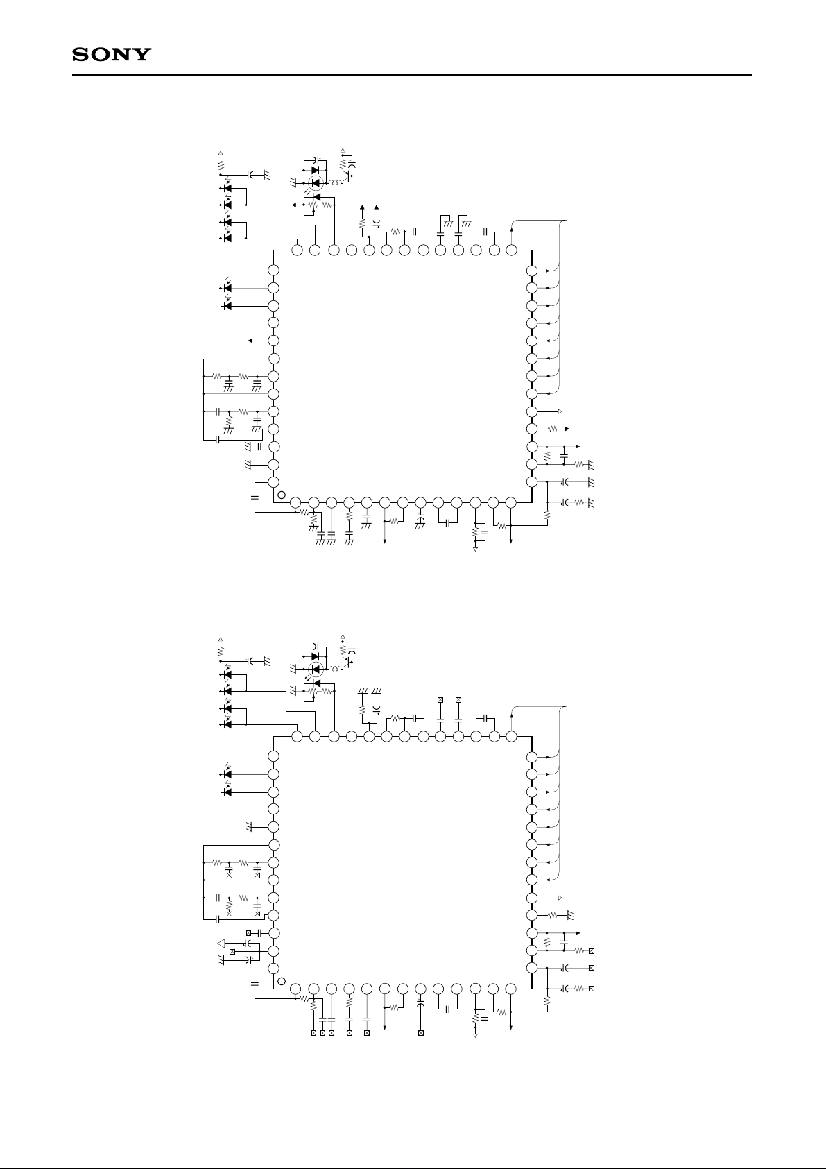
Application Circuit 1 (±2.5V power supply)
CXA1992R
1k
100k
0.01µ
0.047µ
330k
0.022µ
Vcc
A
C
B
D
F
E
VEE
150k
0.01µ
47k
470p
0.022µ
3.3µ
0.1µ
40
41
42
43
44
45
46
47
48
49
50
51
52
V
EE
39
FE_BIAS
F
E
EI
V
EE
TEO
LPFI
TEI
ATSC
TZC
TDFCT
VC
FZC
1
10k
10k
2200p
PD2
FEO
500
Vcc
1µ
22
100µ
10µH
LD
PD
VEE VEE
100
37
38
PD
PD1
FDFCT
FEI
2
3
680k
0.1µ
36
4
LD
FGD
0.1µ
1µ
0.01µ
22k
1M
35
5
RFTC
FLB
0.1µ
DRIVER
34
FE_O
6
RF_M
100k
33
7
RF_O
FE_M
32
RF_I
SRCH
8
4.7µ
0.033µ
31
CP
TGU
9
0.033µ
0.01µ
30
10
CB
TG2
510k
Vcc
0.033µ
29
FSET
11
CC1
28
CC2
TA_M
12
100k
0.015µ
27
FOK
SENS2
SENS1
C. OUT
XRST
DATA
XLT
CLK
LOCK
Vcc
ISET
SL_O
SL_M
SL_P
TA_O
13
DRIVER
26
25
24
23
22
21
20
19
18
17
16
15
14
60k
0.015µ
100k
82k
Vcc
3.3µ
22µ
MICRO
COMPUTER
DSP
V
EE
DRIVER
8.2k
15k
Application Circuit 2 (Single +5V power supply)
10k
10k
PD2
FEO
500
Vcc
1µ
22
100µ
10µH
LD
PD
100
1M
37
38
36
LD
PD
PD1
FDFCT
FEI
FGD
4
2
3
680k
0.1µ
0.1µ
2200p
100k
0.01µ
0.047µ
0.022µ
CC
V
1k
330k
Vcc
A
C
B
D
F
E
150k
0.01µ
47k
470p
10µ
10µ
0.022µ
3.3µ
0.1µ
40
41
42
43
44
45
46
47
48
49
50
51
52
39
FE_BIAS
F
E
EI
V
EE
TEO
LPFI
TEI
ATSC
TZC
TDFCT
VC
FZC
1
35
5
RFTC
FLB
0.1µ
DRIVER
1µ
34
FE_O
6
22k
RF_M
100k
33
7
0.01µ
RF_O
FE_M
32
SRCH
8
4.7µ
RF_I
0.033µ
31
CP
TGU
9
0.033µ
0.01µ
30
10
CB
TG2
510k
Vcc
0.033µ
29
FSET
11
CC1
28
CC2
TA_M
12
100k
0.015µ
27
SENS2
SENS1
C. OUT
XRST
DATA
XLT
CLK
LOCK
ISET
SL_O
SL_M
SL_P
TA_O
13
DRIVER
FOK
Vcc
MICRO
COMPUTER
DSP
26
25
24
23
22
21
20
19
Vcc
18
60k
17
100k
82k
3.3µ
22µ
0.015µ
8.2k
15k
DRIVER
16
15
14
Application circuits shown are typical examples illustrating the operation of the devices. Sony cannot assume responsibility for
any problems arising out of the use of these circuits or for any infringement of third party patent and other right due to same.
– 15 –
Page 16
CXA1992R
Description of Functions
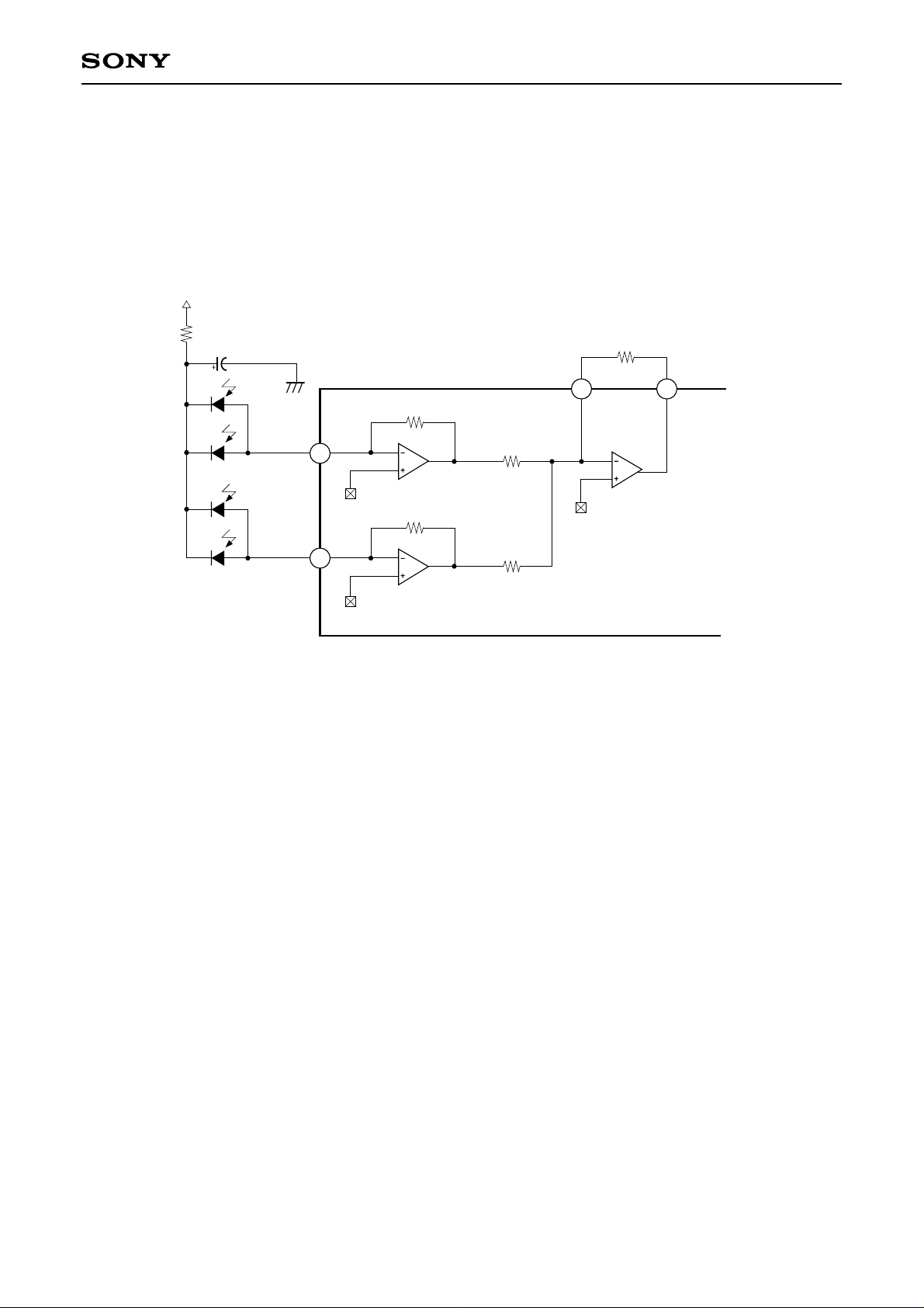
RF Amplifier
The photo diode currents input to the input pins (PD1 and PD2) are each I-V converted through a 58kΩ
equivalent resistor by the PD I-V amplifiers. These signals are added by the RF summing amplifier, and the
photo diode (A + B + C + D) current-voltage converted voltage is output to the RFO pin. An eye-pattern check
can be performed at this pin.
1k
3.3µ
A
C
B
D
iPD1→
iPD2→
PD1
PD2
38
39
VC
VC
58k
PD1 IV AMP
58k
PD2 IV AMP
VA
VB
10k
10k
22k
RF_M
34
RF SUMMING AMP
VC
RF_O
33
The low frequency component of the RFO output voltage is VRFO = 2.2 × (VA + VB) = 127.6kΩ × (iPD1 + iPD2).
– 16 –
Page 17
Focus Error Amplifier
CXA1992R
PD2
B + D
PD1
A + C
EF_BIAS
R3
58k
R5
32k
39
VC
38
VC
VCC
×1
40
VEE
VB
PD2 IV AMP
R2
58k
VA
PD1 IV AMP
×8
×4
×2
IFB3
IFB2
IFB1
RESET : IFB1 to IFB6 ON
R4
32k
×32
×16
IFB5
IFB4
25mV/STEP
R1
4k
IFB6
FE AMP
R6
174k
VC
R7
174k
VC
VC
20mV
–20mV
FOCUS
PHASE
COMPENSATION
VIN > VH L
VIN < VH H
VH
VIN
VL
VIN > VL H
VIN < VL L
FOH
FOL
R8
100k
SENS
SELECTOR
VC
25
26
1
2
7
6
FEO
FEI
R9
10k
FE_M
FE_O
SENS1
SENS2
GND
R10
10k
R11
100k
GND
C1
2200p
DRIVER
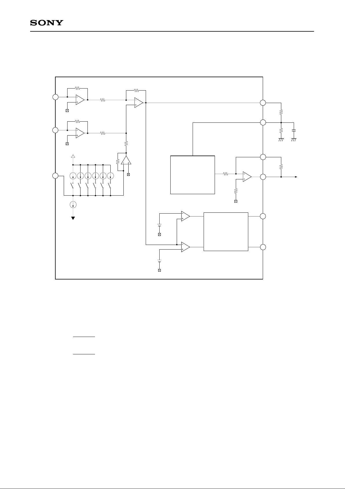
The focus error amplifier calculates the difference between output VA and VB of the RF I-V amplifier, and
output current-voltage converted voltage of the photo diode (A + C – B – D).
The FEO output voltage:
=
174kΩ
32kΩ
174kΩ
32kΩ
(VA – VB)
{(–58kΩ × iPD1) – (–58kΩ × iPD2)}
VFEO =
= 315.4kΩ (iPD2 – iPD1)
The focus error amplifier has a built-in bias adjustment circuit to enable software-based automatic adjustment.
The focus bias adjustment is performed by turning the focus bias adjustment switches (IFB1 to IFB6) ON and
OFF.
The 6-bit focus bias adjustment switches are controlled with commands.
IFB1 to IFB6 are all ON after a reset.
The voltage is varied by approximately 25mV per step.
– 17 –
Page 18
CXA1992R
• Focus error amplifier offset adjustment (when adjusting the IC offset)
The offset adjustment is performed by comparing the FEO when the focus servo is OFF with the reference
level.
The FEO and reference level are compared by the window comparator, and the comparison results are output
from SENS1 and SENS2. (ADDRESS
D11
001110D6)
Adjust the offset so that SENS1 and SENS2 are both High.
Set the reference level to the center ±20mV.
25mV < 40mV < 50mV
Reference level width
Variable voltage per step Variable voltage per 2 steps
• Focus bias fine adjustment
Fine adjustment is performed by turning the focus bias adjustment switches (IFB1 to IFB6) ON and OFF while
monitoring a DSP jitter meter with the microcomputer.
The 6-bit focus bias adjustment switches are controlled with commands.
• When performing conventional focus bias adjustment
Fix the focus bias adjustment switches to the desired settings. (for example, IFB6 ON)
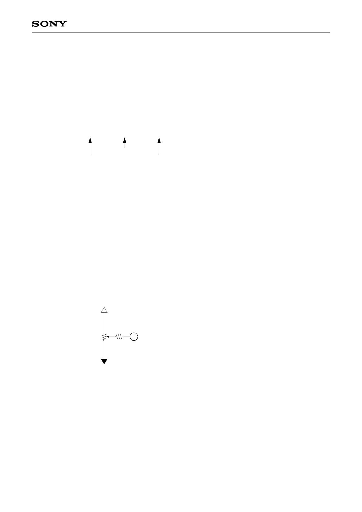
In this condition, adjust the focus bias by turning a volume connected to FE_BIAS (Pin 40).
[Example circuit]
VCC
40
Volume 47k
3.9k
VEE
FE_BIAS
– 18 –
Page 19
Tracking Error Amplifier
R23
R24
100k
150k
C3
0.01µC40.01µ
CXA1992R
R21
TOG3
45
3.3k
TOG4
GND GND
R22
1.5k
LPFI
46
VC
–
+
VC
VC
300mV
VC
20mV
VIN
–20mV
400mV
VIN
VH
VL
VIN > VL H
VIN < VL L
VIN > VH L
VIN < VH H
VH
VL
VIN > VL H
VIN < VL L
VIN > VH L
VIN < VH H
BALH
BALL
TGH
TGL
COMAND
COMAND
CONTROL
CONTROL
SENS
SELECTOR
20
25
26
23
22
21
SENS1
SENS2
XRST
DATA
XLT
CLK
CPU
E
F
41
F I-V AMP
42
E I-V AMP
TEO
R2
260k
C2
12p
VC
12p
VC
R5
13k
R3
26k
R9
VC
VF
R1
260k
C1
VE
43
17k
R8
17k
R4
6.8k
V
R7
R6
75k
110k
VC
EI
R14
13k
R13
13k
R12
96k
R10
BAL1
NORMAL
GAIN UP
GAIN UP
VC
56k
27k
R11
BAL2
TE AMP
TGFL
TGFL
NORMAL
13k
R15
BAL3
BAL4
R16
96k
R18
7.5k
10k
R17
16k
R20
7.5k
R19
TOG2
TOG1
VC
RE
The difference between E I-V amplifier output VE and F I-V amplifier output VF is taken and output from TEO.
The tracking error amplifier has built-in balance and gain adjustment circuits to enable software-based
automatic adjustment.
The balance adjustment is performed by varying the combined resistance value of the T-configured feedback
resistance at the E I-V amplifier.
E I-V AMP feedback resistance = R1 + R4 +
E I-V AMP feedback resistance = R2 + R5 + = 403kΩ
R1 × R4
RE
R2 × R5
R3
Vary the combined resistance value of the E I-V amplifier's feedback resistance by using the balance
adjustment switches (BAL1 to BAL4).
The gain adjustment is performed by resistance dividing the TE AMP output by the gain adjustment switches
(TOG1 to TOG4).
The balance and gain adjustment switches are controlled with commands.
Set the cut-off frequency of the external LPF between 10Hz to 100Hz.
– 19 –
Page 20
CXA1992R
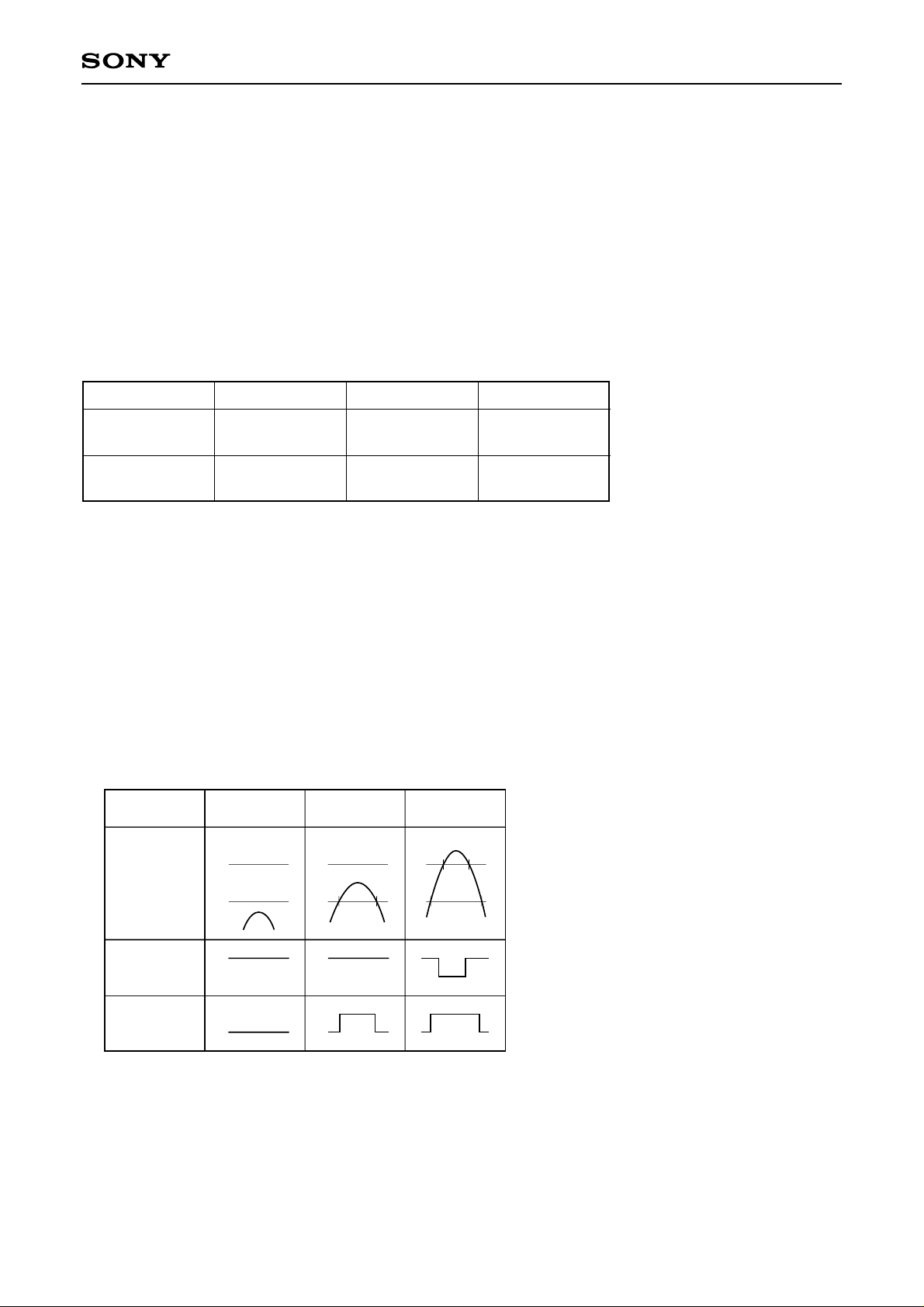
• Balance adjustment
The balance adjustment is performed by passing the tracking error signal (TEO signal) through the external
LPF, extracting the offset DC, and comparing it to the reference level.
However, the TEO signal frequency distribution ranges form DC to 2kHz. Merely sending the signal through
the LPF leaves lower frequency components, and the complete offset DC can not be extracted.
To extract it, monitor the TEO signal frequency at all times, and perform adjustment only when a frequency
that can lower a sufficient gain appears on the LPF.
Use the C.OUT output to check this frequency.
The offset DC and reference level are compared by the window comparator.
The comparison signal is output from the SENS1 and SENS2 pins. (ADDRESS
D11
001100D6)
Adjust the balance so that the SENS1 and SENS2 pins are both High.
VIN < VL < VH VL < VIN < VH VL < VH < VIN
SENS1 pin
BALH
SENS2 pin
BALL
H
L
H
H
L
H
VH: High level threshold value
VIN: Window comparator input signal
VL: Low level threshold value
• Gain adjustment
Gain adjustment is performed by passing the TEO signal through the HPF and comparing the AC component
to the reference level.
The AC component is generated by taking the difference between TE and the offset DC input to Pin 46.
The AC component and reference level are compared by the window comparator.
The comparison signal is output from the SENS1 and SENS2 pins. (ADDRESS
D11
001101D6)
The comparison signal is as follows.
(1) (2) (3)
VH
VL
VIN
SENS1 pin
TGH
SENS2 pin
TGL
H H
L
The gain should be adjusted so that the SENS1 and SENS2 pins are as shown in status (2).
When the TEO signal level is low and TGH (SENS1 pin) does not go Low, the gain should be raised with the
TGFL command for adjustment. If the adjustment does not bring the result of Low, check the pulse duty of TGL
(SENS2 pin).
– 20 –
Page 21
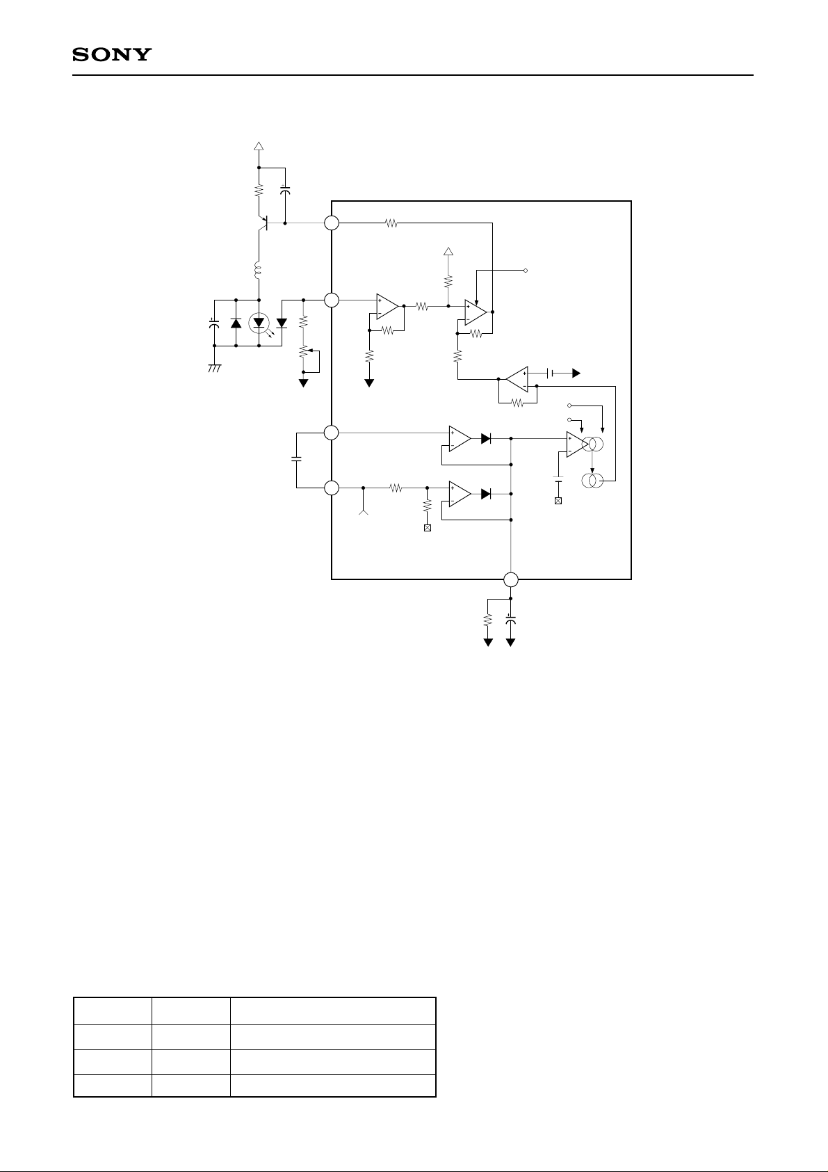
APC & Laser Power Control
CXA1992R
VCC
C1
LD PD
C3
0.01µ
R2
500
100µ
C2
LD
130mV
PD
100
VEE
RF_I
RF_O
R3
36
37
1.1Vpp
32
1.47V
33
RF
VEE
R4
10k
R5
55k
R7
39.5k
R6
1k
R9
23.5k
R8
10k
VC
VCC
R11
10k
R10
56k
LDON
R12
56k
V
L
R14
5.3k
VREF
VEE
LPC ON/OFF
30%/10%
670mV
VC
35
R1
22
L1
10µH
1µ
GND
R13
1M
RFTC
C4
1µ
VEEVEE
• APC
When the laser diode is driven by a constant current, the optical power output has extremely large negative
temperature characteristics.
The APC circuit is used to maintain the optical power output at a constant level.
The laser diode current is controlled according to the monitor photo diode output.
• Laser power control
The RF level is stabilized by attaching an offset to the APC VL and controlling the laser power in sync with the
RF level fluctuations.
The RF_O and RF_I levels are compared and the larger of the two is smoothed by the RFTC's external CR.
This signal is then compared with the reference level.
The laser power is controlled by attaching an offset to VL according to the results of comparison with the
reference level.
Set the reference level to 670mV. (center voltage reference)
LPC ON/OFF and LD ON/OFF control is performed with commands.
The laser power control limit can also be switched between ±10% and ±30% with commands.
LPC
LPCL VL variable range
OFF
ON
ON
—
±30%
±10%
Approximately 1.27V
Approximately 1.27V ± 265mV
Approximately 1.27V ± 88mV
– 21 –
Page 22
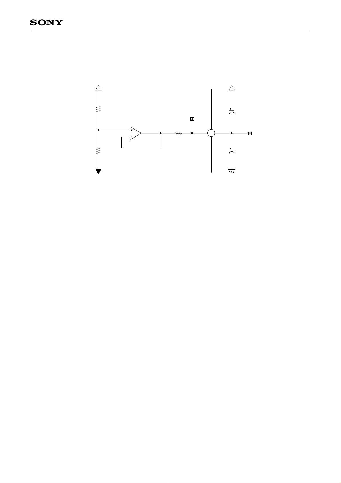
Center Voltage Generation Circuit
(The figure below shows a single voltage application; Connect to GND for dual power supplies.)
Maximum current is approximately ±3mA. Output impedance is approximately 50Ω.
CXA1992R
VCC
30k
30k
VEE
Connected internally to the V
EE pin.
50
VC
51
VCC
VC
GND
– 22 –
Page 23

Focus Servo
0.022µ
10k
10k
2200p
0.1µ
680k
0.1µ
52
1
2
3
4
FZC
FEO
FE
FEI
100k
FDFCT
FGD
9k
51k
75k
DFCT
FS3
FS4
FZC
68k
FLB
SENS
SELECTOR
Focus
phase
Compensation
40k
FSET
5
11
100k
50k
FS2
50k
8
11µ 22µ
SRCH
FE_O
FE_M
FS1
Charge
up
25
6
7
17
SENS1
100k
ISET
CXA1992R
FOCUS COIL
60k
0.1µ
510k
0.015µ
4.7µ
The above figure shows a block diagram of the focus servo.
Ordinarily the FE signal is input to the focus phase compensation circuit through a 68kΩ resistance; however,
when DFCT is detected, the FE signal is switched to pass through a low-pass filter formed by the internal
100kΩ resistance and the capacitance connected to Pin 3. When this DFCT prevention circuit is not used,
leave Pin 3 open. The defect switch operation can be enabled and disabled with command.
The capacitor connected between Pin 5 and GND is a time constant to boost the low frequency in the normal
playback state.
The peak frequency of the focus phase compensation is approximately 1.2kHz when a resistance of 510kΩ is
connected to Pin 11.
The focus search height is approximately ±1.1Vp-p when using the constants indicated in the above figure.
This height is inversely proportional to the resistance connected between Pin 17 and VEE. However, changing
this resistance also changes the height of the track jump and sled kick as well.
The FZC comparator inverted input is set to 15% of Vcc and VC (Pin 51); (Vcc – VC) × 15%.
∗
510kΩ resistance is recommended for Pin 11.
– 23 –
Page 24
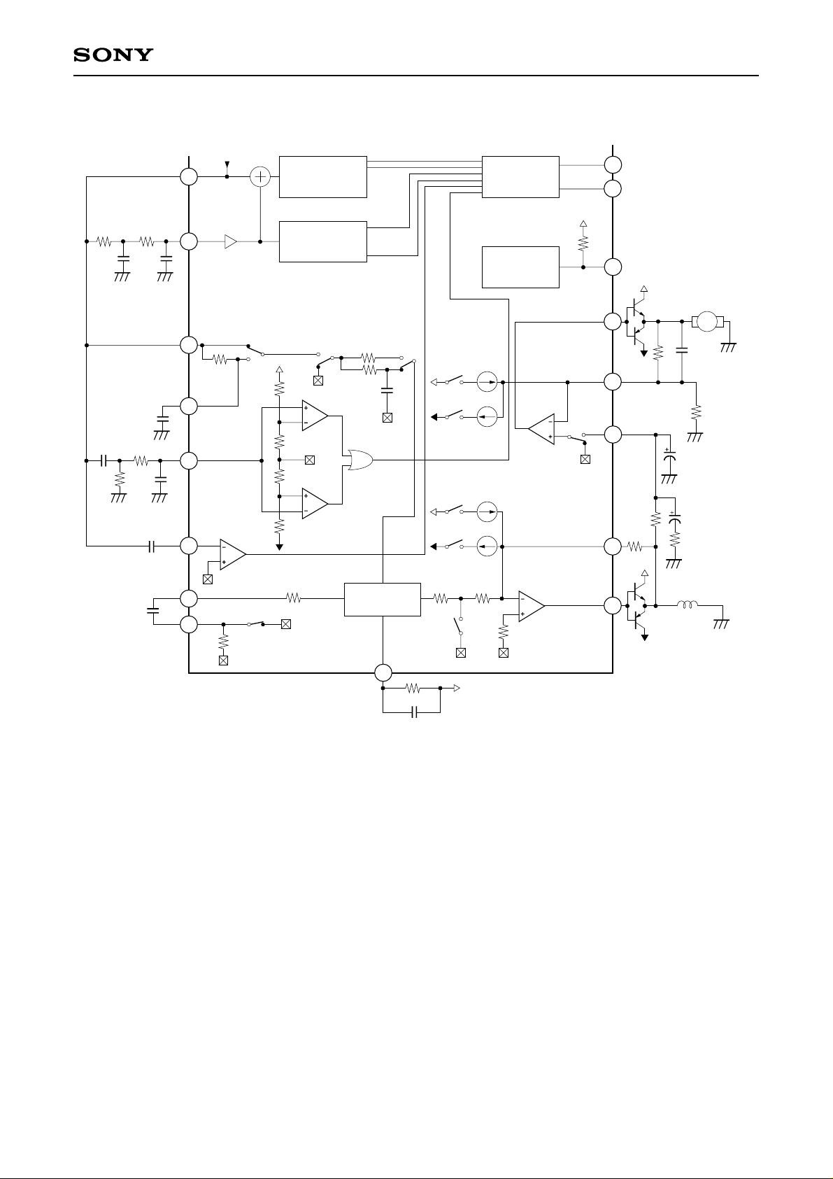
Tracking and Sled Servo
CXA1992R
0.047µ
0.033µ
150k100k
0.01µ
47k
330k
0.022µ
45
TEO
BUFFER AMP
46
LPFI
0.01µ
TEI
47
100k
TDFCT
50
0.1µ
ATSC
48
470p
TZC
49
TGU
9
TG2
10
TE
+
–
TZC
470k
DFCT
TG2
GAIN
WINDOW
COMPARATOR
BALANCE
WINDOW
COMPARATOR
TM1
100k
1k
1k
100k
20k
Tracking Phase
Compensation
680k
680k
TGH
TGL
BALH
BALL
ATSC
11
TG1
66p
FSET
TM6
22µA
TM5
22µA
TM4
11µA
TM3
11µA
10k 90k
TM7
SENS
SELECTOR
SLED ON/OFF
CONTROL
47k
SL_O
TM2
TA_M
TA_O
26
25
19
16
15
14
12
13
SENS2
SENS1
LOCK
SL_M
SL_P
82k
100k
SLED MOTOR
M
120k
0.015µ
8.2k
3.3µ
22µ
15k
TRACKING
COIL
510k
0.015µ
The above figure shows a block diagram of the tracking and sled servo.
The capacitor connected between Pins 9 and 10 is a time constant to cut the high-frequency gain when TG2 is
OFF. The peak frequency of the tracking phase compensation is approximately 1.2kHz when a 510kΩ
resistance is connected to Pin 11. In the CXA1992R, TG1 and TG2 are inter-linked switches.
To jump tracks in FWD and REV directions, turn TM3 or TM4 ON. During this time, the peak voltage applied to
the tracking coil is determined by the TM3 or TM4 current and the feedback resistance from Pin 12. To be
more specific,
Track jump peak voltage = TM3 (or TM4) current × feedback resistance value
The FWD and REV sled kick is performed by turning TM5 or TM6 ON. During this time, the peak voltage
applied to the sled motor is determined by the TM5 or TM6 current and the feedback resistance from Pin 15;
Sled kick peak voltage = TM5 (or TM6) current × feedback resistance
The values of the current for each switch are determined by the resistance connected between Pin 17 and VEE.
When this resistance is 60kΩ :
TM3 (or TM4) = ±11µA, and TM5 (or TM6) = ±22µA.
As is the case with the FE signal, the TE signal is switched to pass through a low-pass filter formed by the
internal resistance (100kΩ) and the capacitance connected to Pin 50.
– 24 –
Page 25
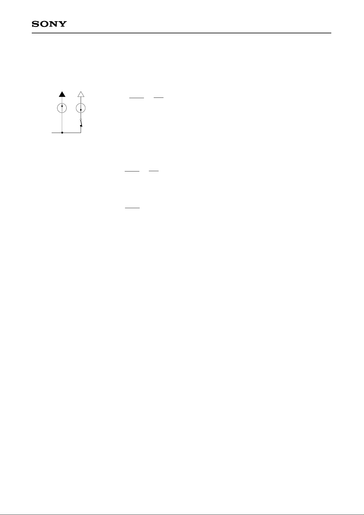
CXA1992R
The ISET pin is used to connect external resistance. This external resistance sets the current which
determines the focus search, track jump, and sled kick heights.
• Focus search current
VBG
I1 = ×
2I1
I
R
1
2
(VBG: approximately 1.27V)
I2 = 2I1
FS1
• Track jump current (TM3 and TM4 current)
VBG
I = ×
R
1
2
• Sled kick current (TM5 and TM6 current, when D1 = D0 = 0 during 1X$ commands)
VBG
I =
R
Use external resistance of between 30kΩ to 240kΩ.
Using external resistance outside this range may cause oscillation.
– 25 –
Page 26
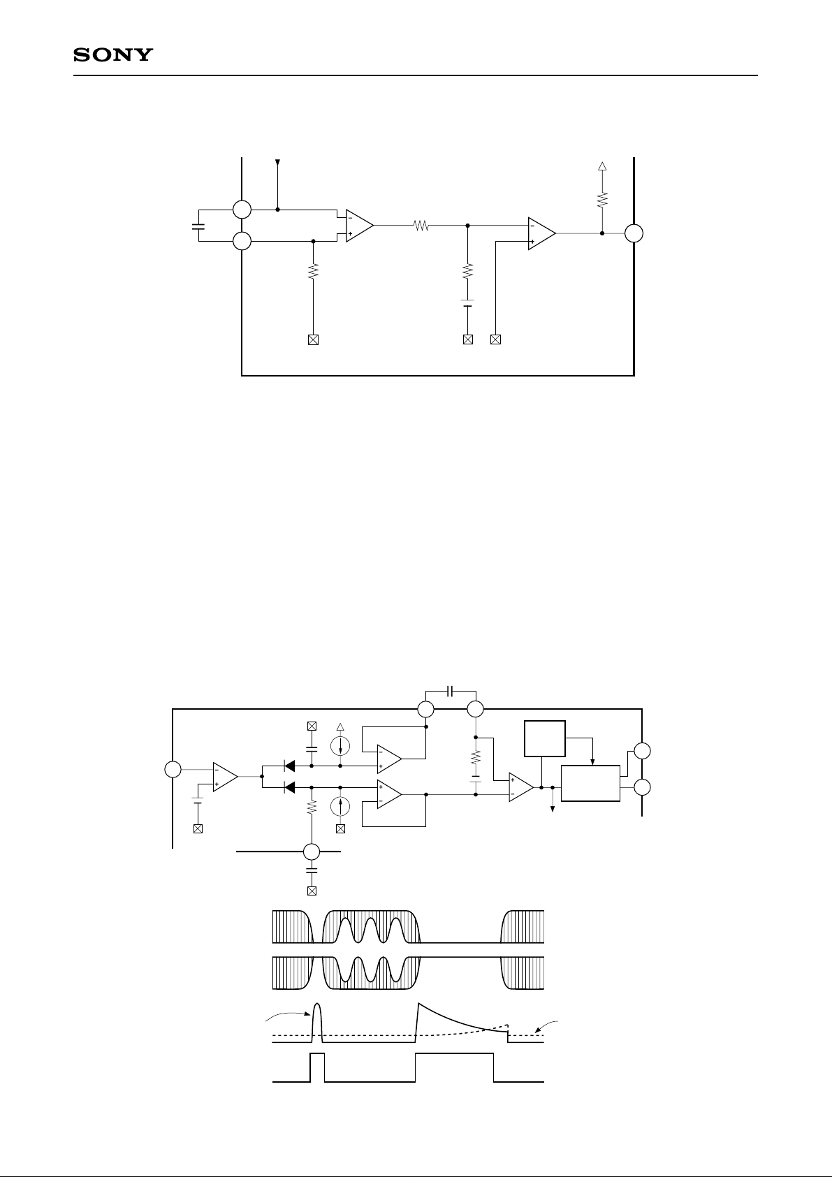
Focus OK Circuit
CXA1992R
C5
0.01µ
RF_O
RF_I
33
32
RF
54k
× 1
VG
20k
V
CC
FOK
27
15k 92k
0.63V
FOCUS OK AMP FOCUS OK
COMPARATOR
The focus OK circuit creates the timing window okaying the focus servo from the focus search state.
The HPF output is obtained at Pin 32 from Pin 33 (RF signal), and the LPF output (opposite phase) of the
focus OK amplifier output is also obtained.
The focus OK output is inverted when VRFI – VRFO ≈ –0.37V.
Note that, C5 determines the time constant of the HPF for the mirror circuit and the LPF of the focus OK
amplifier. Ordinarily, with a C5 equal to 0.01µF selected, the fc is equal to 1kHz, and block error rate
degradation brought about by RF envelope defects caused by scratched discs can be prevented.
Defect Circuit
After the RFI signal is reverted, two time constants, long and short, are held at bottom. The short time constant
bottom hold responds to 0.1ms or greater disc mirror defects, and the long time constant bottom hold holds the
pre-defect mirror level. By differentiating and level-shifting these constants with capacitor coupling and
comparing both signals, the mirror defect detection signal is generated.
0.033µ
CC1 CC2
28
FLIP
FLOP
c
d
DEFECT COMPARATOR
e
DFCT1
DEFECT SW
DFCT2
SENS
SELECTOR
26
25
SENS2
SENS1
RF_O
33
a
× 2
DEFECT AMP
RFO
a
b
DEFECT
AMP
29
b
DEFECT BOTTOM
CB
30
HOLD
0.01µ
c
e
BOTTOM
HOLD (1)
solid line
CC1
DFCT1
– 26 –
H
L
d
BOTTOM
HOLD (2)
dotted line
CC2
Page 27
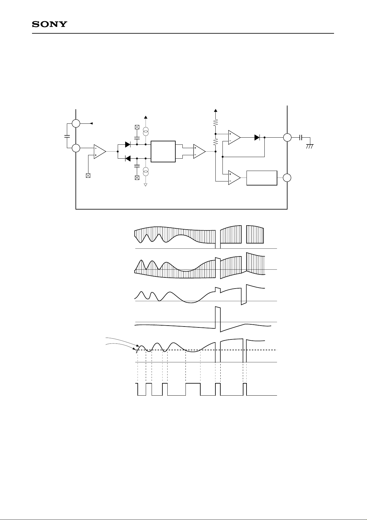
CXA1992R
Mirror Circuit
The mirror circuit performs peak and bottom hold after the RFI signal has been amplified.
The peak and bottom holds are both held through the use of a time constant. For the peak hold, a time
constant can follow a 30kHz traverse, and, for the bottom hold, one can follow the rotation cycle envelope
fluctuation.
RF_O
RF_I
33
32
RF
× 1.4
G
MIRROR AMP
RF_O
G
(RF_I)
H
(PEAK HOLD)
PEAK &
BOTTOM
HOLD
MIRROR HOLD AMP
0.033µ
31
0V
0V
0V
26
CP
SENS2
H
× 1
J
I
MIRR
MIRROR
COMPARATOR
K
SENS
SELECTOR
(BOTTOM HOLD)
I
J
K
(MIRROR HOLD)
MIRR
0V
H
L
The DC playback envelope signal J is obtained by amplifying the difference between the peak and bottom hold
signals H and I. Signal J has a large time constant of 2/3 its peak value, and the mirror output is obtained by
comparing it to the peak hold signal K. Accordingly, when on the disc track, the mirror output is Low; when
between tracks (mirrored portion), it is High; and when a defect is detected, it is High. The mirror hold time
constant must be sufficiently large compared with the traverse signal.
In the CXA1992R, this mirror output is used only during braking operations, and no external output pin is
attached. Accordingly, when connecting DSP with MIRR input pin, input the C.OUT output to the MIRR input of
the DSP.
– 27 –
Page 28
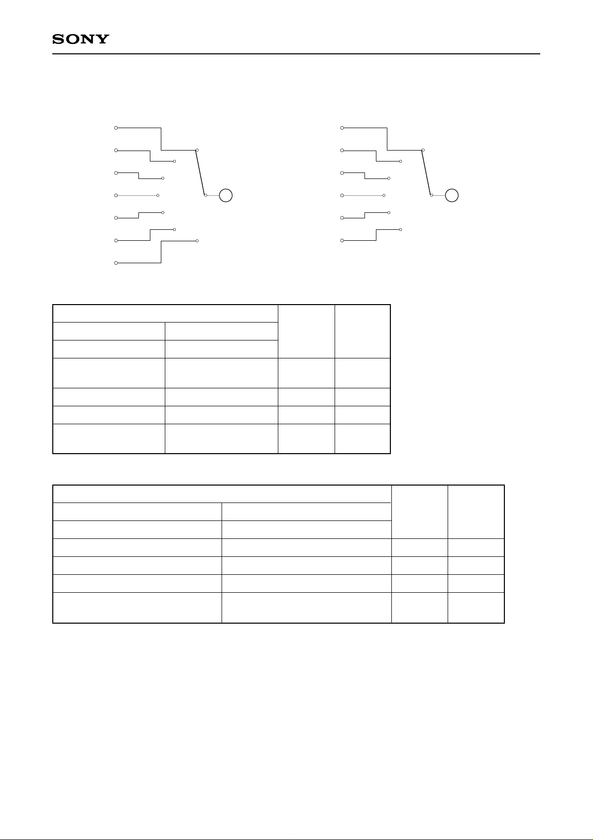
SENS Selector
CXA1992R
FZC
DFCT1
TZC
BALH
TGH
FOH
ATSC
25
SENS1
HIGH-Z
DFCT2
MIRR
BALL
TGL
FOL
26
SENS2
What is output to the SENS1 and SENS2 pins varies according to the address input to the DATA pin.
DATA (Pin 22) 8-bit transfer
ADDRESS
D7
D6 D5 D4 D3 D2 D1 D0
0
0
0
0
X
0
0
0
1
X
DATA
X
X
SENS1 SENS2
X
X
X
X
FZC
DFCT1
H
(HIGH-Z)
DFCT2
0
0
1
0
X
X
X
X
0
1
0
0
X
X
X
X
1
1
1
1
X
X
X
X
TZC
H
(HIGH-Z)
MIRR
H
(HIGH-Z)
DATA (Pin 22) 12-bit transfer
ADDRESS
D11
D10 D9 D8 D7 D6 D5 D4 D3 D2 D1 D0
0
0
1
1
0
0
X
X
0
0
1
1
0
1
X
X
0
0
1
1
1
0
X
X
0
0
1
1
1
1
X
X
DATA
X
X
X
X
SENS1 SENS2
X
X
X
X
X
X
X
X
X
X
X
X
BALH
TGH
FOH
ATSC
BALL
TGL
FOL
H
(HIGH-Z)
Notes)
• 12-bit transfer should be performed during $3XX commands. When 8 bits are transferred, SENS1 and
SENS2 are switched according to the D3 and D2 data.
• SENS1 and SENS2 are switched without latching.
– 28 –
Page 29
CXA1992R
Commands
The input data to operate this IC is configured as 8-bit/12-bit data; however, below, this input data is
represented by 2-digit hexadecimal numerals in the form $XX, where X is a hexadecimal numeral between 0
and F/$XXX for 12-bit.
Commands for the CXA1992R can be broadly divided into four groups ranging in value from $0X, $1X, $2X,
$3XX.
1. $0X (FZC at SENS1 pin (Pin 25), H (Hi-Z) at SENS2 pin (Pin 26))
These commands are related to focus servo control.
The bit configuration is as shown below.
D7 D6 D5 D4 D3 D2 D1 D0
0 0 0 0 FS4 — FS2 FS1
Four focus related switches exist: FS1, FS2, FS4 and DFCT.
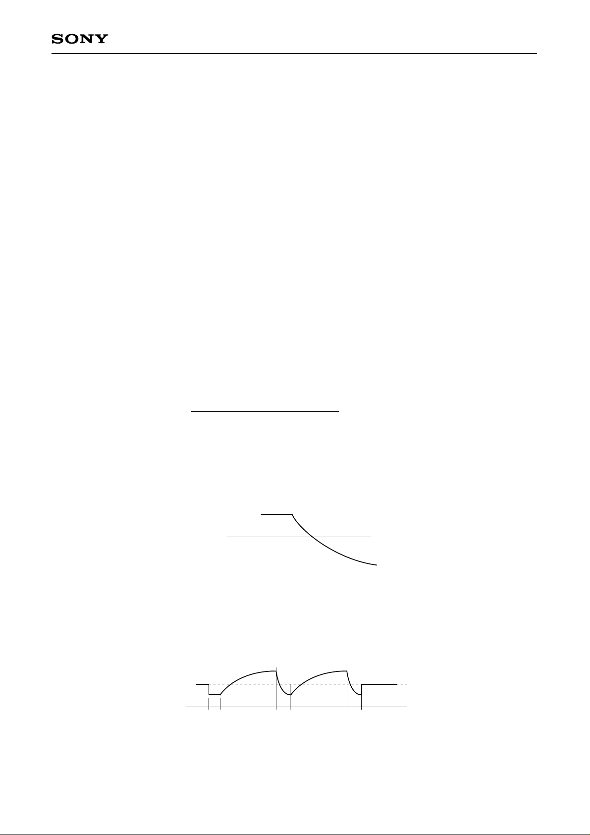
$00 When FS1 = 0, Pin 8 is charged to (22µA – 11µA) × 50kΩ = 0.55V.
If, in addition, FS2 = 0, this voltage is no longer transferred, and the output at Pin 6 becomes 0V.
$02 From the state described above, the only FS2 becomes 1. When this occurs, a negative signal is output
to Pin 6. This voltage level is obtained by equation 1 below.
(22µA – 11µA) × 50kΩ × .... Equation 1
resistance between Pins 6 and 7
50kΩ
The SRCH DOWN speed can be increased by the charge up circuit.
$03 From the state described above, FS1 becomes 1, and a current source of +22µA is split off.
Then, a CR charge/discharge circuit is formed, and the voltage at Pin 8 decreases with the time as
shown in Fig. 1 below.
0V
Fig. 1. Voltage at Pin 8 when FS1 goes from 0 → 1
This time constant is obtained with the 50kΩ resistance and an external capacitor.
By alternating the commands between $02 and $03, the focus search voltage can be constructed. (Fig. 2)
0V
$0002
03 02 03 0002
Fig. 2. Constructing the search voltage by alternating between $02 and $03. (Voltage at Pin 6)
– 29 –
Page 30
CXA1992R
1-1. FS4
This switch is provided between the focus error input and the focus phase compensation, and is in charge of
turning the focus servo ON and OFF.
$00 → $08
Focus off Focus on
1-2. Procedure of focus activation
For description, suppose that the polarity is as described below.
a) The lens is searching the disc from far to near;
b) The output voltage (Pin 6) is changing from negative to positive; and
c) The focus S-curve is varying as shown below.
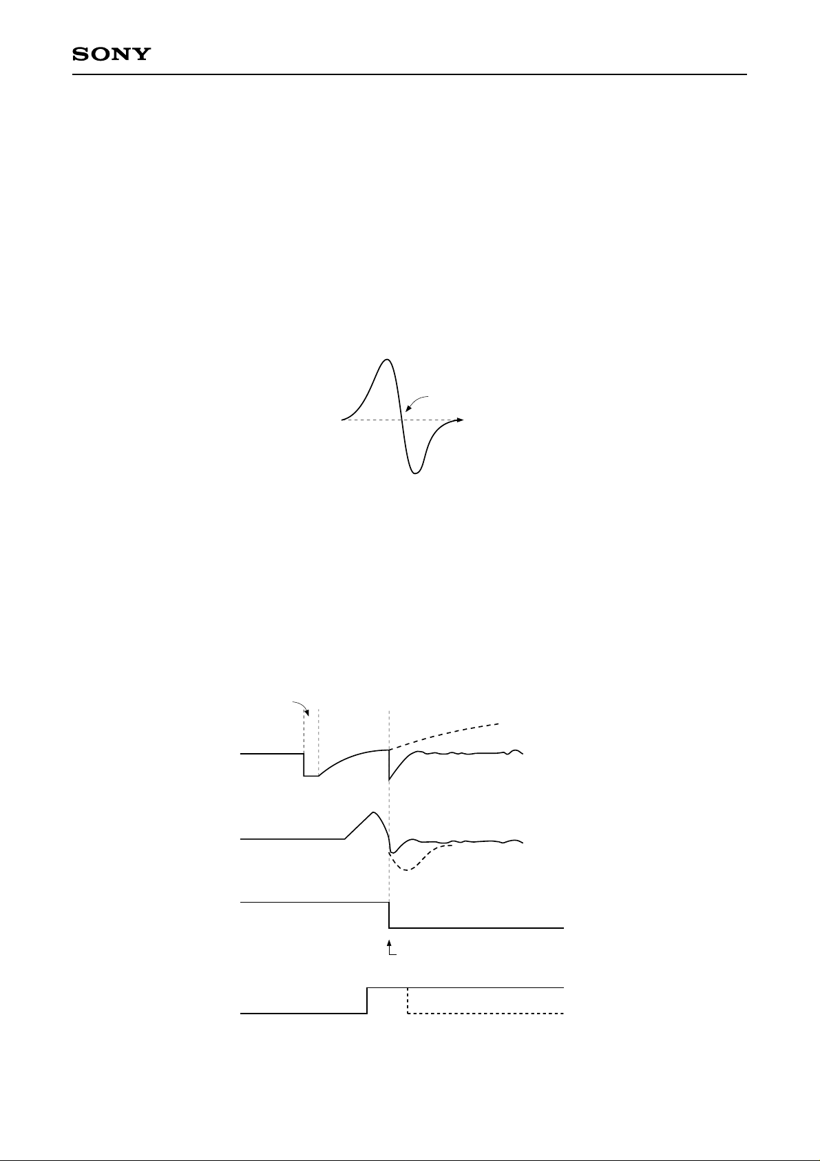
A
t
Fig. 3. S-curve
The focus servo is activated at the operating point indicated by A in Fig. 3. Ordinarily, focus searching and the
turning the focus servo switch ON are performed during the focus S-curve transits the point A indicated in Fig.
3. To prevent misoperation, this signal is ANDed with the focus OK signal.
In this IC, FZC (Focus Zero Cross) signal is output from the SENS1 pin (Pin 25) as the point A transit signal.
In addition, focus OK is output as a signal indicating that the signal is in focus (can be in focus in this case).
Following the line of the above description, focusing can be well obtained by observing the following timing
chart.
(20ms) (200ms)
$02
Drive voltage
Focus error
$03($00)
$08
∗
The broken lines in the figure
indicate the voltage assuming
the signal is not in focus.
SENS1
(FZC)
Focus OK
The instant when the signal is brought into focus.
Fig. 4. Focus ON timing chart
– 30 –
Page 31

CXA1992R
Note that the time from the High to Low transition of FZC to the time command $08 is asserted must be
minimized. To do this, the software sequence shown in B is better than the sequence shown in A.
FZC ↓ ?
YES
F. OK ?
YES
Transfer $08
Latch
(A) (B)
NO
NO
Fig. 5. Poor and good software command sequences
2. $1X (DFCT1 at SENS1 pin (Pin 25), DFCT2 at SENS2 pin (Pin 26))
These commands deal with switching TG1/TG2, brake circuit ON/OFF,
and the sled kick output.
The bit configuration is as follows:
D7 D6 D5 D4 D3 D2 D1 D0
0 0 0 1 TG1, TG2 Break Sled kick
circuit height
ON/OFF ON/OFF
Transfer $08
F. OK ?
YES
FZC ↓ ?
YES
Latch
NO
NO
Sled kick height
D1
(PS1)
(PS0)
0
0
1
1
D0
0
1
0
1
Relative
value
±1
±2
±3
±4
TG1, TG2, TM7
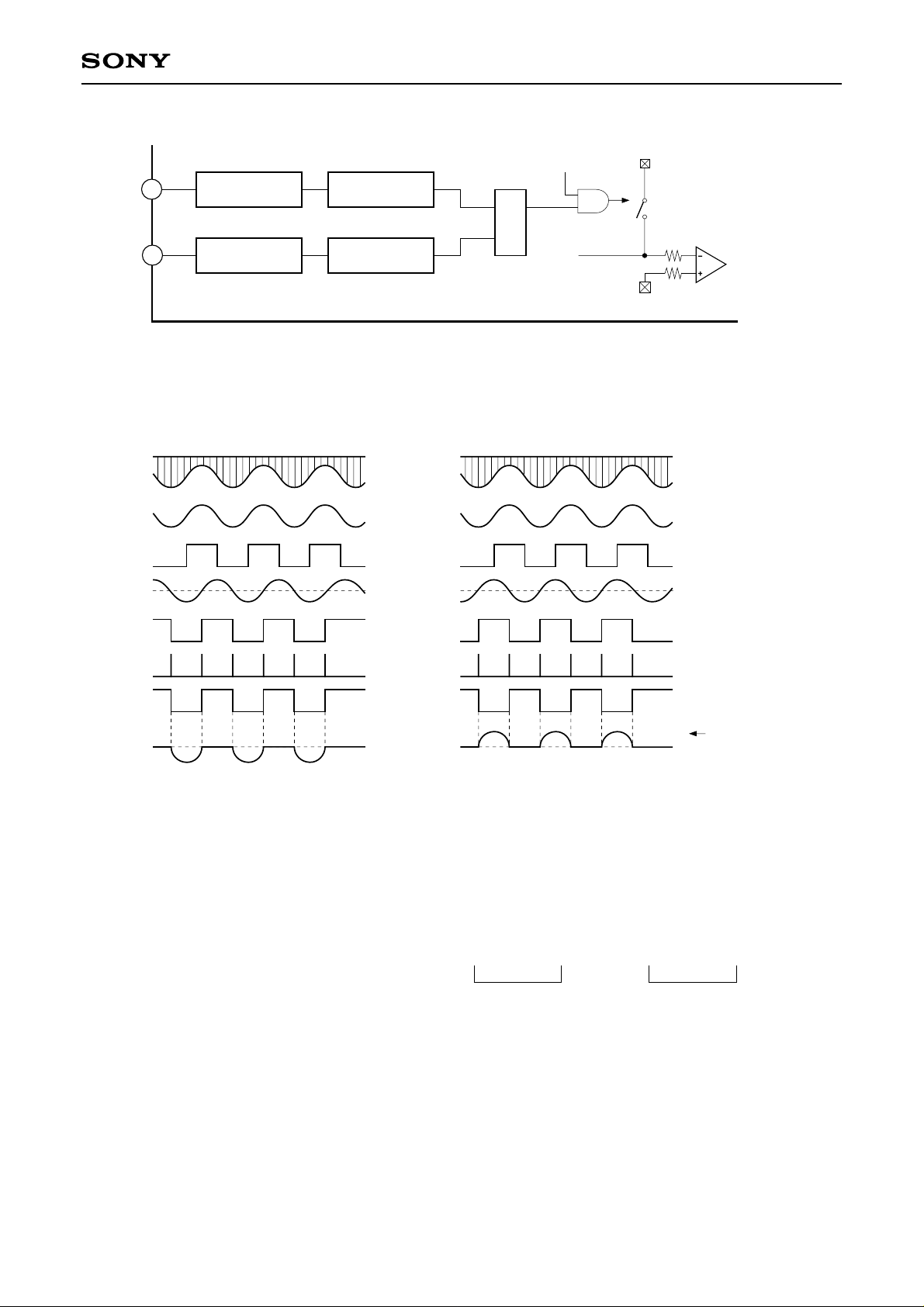
The purpose of TG1 and TG2 is to switch the tracking servo gain Up/Normal. TG1 and TG2 are interlinked
switches. The brake circuit (TM7) is to prevent the frequently occurred phenomena where the merely 10-track
jump has been performed actually though a 100-track jump was intended to be done due to the extremely
degraded actuator settling caused by the servo motor exceeding the linear range after a 100 or 10-track jump.
For the prevention method, when the actuator travels radially; that is, when it traverses from the inner track to
the outer track of the disc and vice versa, the brake circuit utilizes the fact that the phase relationship between
the RF envelope and the tracking error is 180° out-of-phase to cut the unneeded portion of the tracking error
and apply braking.
– 31 –
Page 32
CXA1992R
[∗A]
[∗B]
[∗C]
[∗D]
[∗E]
RF_I
TZC
32
49
[∗A]
Envelope
Detection
[∗D]
Waveform
Shaping
Fig. 6. TM7 movement during braking operation
From inner to outer track
[∗B]
Waveform
Shaping
[∗E]
Edge Detection
(MIRR)
(Latch)
CXA1992
D2
[∗C]
[∗F]
[∗G]
QD
BRK
CK
From outer to inner track
TM7
Low: open
High: make
[∗H]
("MIRR")
("TZC")
[∗F]
[∗G]
Braking is applied
[∗H]
0V
from here.
Fig. 7. Internal waveform
3. $2X (TZC at SENS1 pin (Pin 25), MIRR at SENS2 pin (Pin 26))
These commands deal with turning the tracking servo and sled servo ON/OFF, and creating the jump pulse
and fast forward pulse during access operations.
D7 D6 D5 D4 D3 D2 D1 D0
0 0 1 0 Tracking Sled
control control
00 off 00 off
01 Servo ON 01 Servo ON
10 F-JUMP 10
11 R-JUMP 11
F-FAST FORWARD
R-FAST FORWARD
↓↓
TM1, TM3, TM4, TM2, TM5, TM6
– 32 –
Page 33

CXA1992R
4. $3XX
These commands mainly control the balance and gain control circuit switches used during automatic tracking
adjustment and the bias circuit switch used during automatic focus bias adjustment.
In the initial resetting state, BAL1 to BAL4 switches and TOG1 to TOG4 switches are ON. Also, the IFB1 to 6
switches are ON.
• Balance adjustment
The balance adjustment switches BAL1 to BAL4 can be controlled by setting D6 = 0 and D7 = 0. The switches
are set using D0 to D3.
At this time, SENS1 outputs BALH and SENS2 outputs BALL.
Data is set by specifying switch conditions D0 to D3 and sending a latch pulse with D6 = 0 and D7 = 0.
Sending a latch pulse with D6, D7 ≈ 0 does not change the balance switch settings.
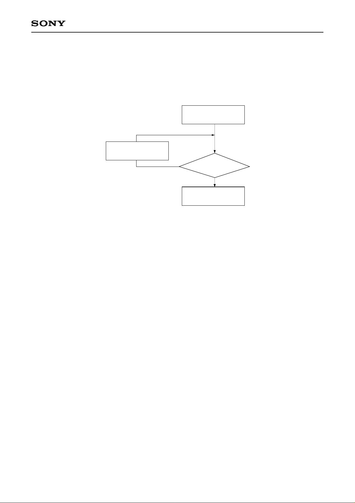
START
C.OUT
BAL1 to BAL4
Switch Control
is the frequency high
enough ?
YES
SENS1/2
Balance OK ?
Adjustment Completed
NO
Balance adjustment
• Gain adjustment
The gain adjustment switches TOG1 to TOG4 can be controlled by setting D6 = 1 and D7 = 0. These switches
are set using D0 to D3.
At this time, SENS1 outputs TGH and SENS2 outputs TGL.
In a fashion similar to the method used with the balance adjustment, set the data by specifying switch
conditions D0 to D3 and sending a latch pulse with D6 = 1 and D7 = 0.
START
TOG1 to TOG4
Switch control
NO
Adjustment Completed
Gain adjustment
– 33 –
SENS1/2
GAIN OK ?
YES
Page 34
CXA1992R
• Focus bias adjustment
The focus bias adjustment switches IFB1 to 6 can be controlled by setting D6 = 0 and D7 = 1. The switches
are set using D0 to D5.
At this time, SENS1 outputs FOH and SENS2 outputs FOL.
Data is set by specifying switch conditions D0 to D5 and sending a latch pulse with D6 = 0 and D7 = 1.
START
IFB1 to 6
Switch Control
SENS1/2
NO
BIAS OK ?
YES
Adjustment Completed
Focus bias adjustment method
• TGFL
The tracking gain can be switched by setting D5 with D6 = 1 and D7 = 0.
The tracking gain is GAIN UP with D5 = 1 and NORMAL GAIN with D5 = 0.
When using a pickup with a low tracking gain, the tracking gain can be raised by approximately 6dB by
setting GAIN UP.
(This command does not raise the gain during playback.)
• LPC
The laser power control circuit can be turned ON and OFF by setting D0 with D6 = 1 and D7 = 1.
The circuit is ON with D0 = 1 and OFF with D0 = 0.
• LPCL
The laser power control limit can be switched between ±10% and ±30% by setting D1 with D6 = 1 and D7 = 1.
The control limit is ±10% with D1 = 0 and ±30% with D1 = 1.
• LDON
The laser diode can be turned ON and OFF by setting D2 with D6 = 1 and D7 = 1.
The laser diode is ON with D2 = 1 and OFF with D2 = 0.
– 34 –
Page 35
CXA1992R
• ATSC
The anti-shock function can be controlled by setting D3 with D6 = 1 and D7 = 1.
This function is disabled with D3 = 1 and enabled with D3 = 0.
At this time, SENS1 outputs ATSC.
Even if ATSC is disabled, ATSC is output to SENS1.
When an anti-shock signal is generated during the enable status, TG1 and TG2 switch to GAIN UP mode.
(In the Block Diagram, TG1 is set to the side and TG2 is OFF. Even if TG1 and TG2 are NORMAL mode,
they switch to GAIN UP mode in conjunction with ATSC.)
When the anti-shock function is not used, Pin 48 (ATSC) should be connected to VC.
• RDFCT2
DFCT2 can be reset by setting D4 with D6 = 1 and D7 = 1.
DFCT2 is reset with D4 = 1.
After a reset, High is held when DFCT1 rises.
During $1X commands, DFCT2 is output from SENS2.
DFCT2 operates even if DFCT is disabled.
Whether or not DFCT rises at the proper timing for the microcomputer can also be confirmed.
• INT
The interruption (scratched disc) countermeasure circuit can be set to operating status by setting D5 with D6
= 1 and D7 = 1.
This circuit is enabled when D5 = 1 and disabled when D5 = 0.
Even if DFCT1 does not rise, this circuit is effective for scratched discs which cause MIRR to rise.
When MIRR rises, the DFCT switch is routed through the low-pass filter.
The interruption countermeasure circuit is forcibly turned OFF regardless of the command when the tracking
gain is increased. (including when the gain is increased by ATSC or LOCK)
Even if DFCT is disabled, the interruption countermeasure circuit operates when INT is enabled.
Parallel direct interface
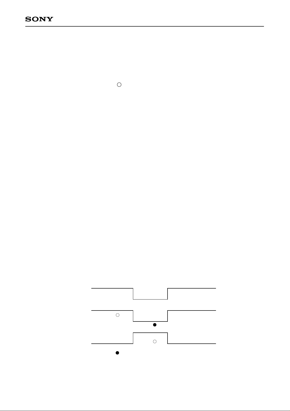
• LOCK (Sled overrun prevention circuit)
This circuit operates when LOCK is low.
When LOCK is low, the sled is OFF, and TG1 and TG2 are UP (TRACKING GAIN UP).
LOCK
SLED
TRACKING GAIN
TM2 SW: side
SLED ON
NORMAL
TG1 SW: side
TG2 ON
TM2 SW: side
SLED OFF
UP
TG1 SW: side
TG2 OFF
– 35 –
Page 36

CPU Serial Interface Timing Chart
CXA1992R
DATA
CLK
XLT
Item
Clock frequency
Clock pulse width
Setup time
Hold time
Delay time
Latch pulse width
Data transfer interval
D0 D1 D2 D3 D4 D5 D6 D7 D0
WCK
t
1/fck
tWCK
tSU
h
t
tCD
tD
tWL
(VCC = 3.0V)
Symbol
fck
fwck
tsu
th
tD
tWL
tCD
Min.
500
500
500
500
1000
1000
Typ. Max. Unit
1
MHz
ns
ns
ns
ns
ns
ns
Low level input voltage
High level input voltage
VIL
VIH
0.0
(VCC – VEE) × 0.9
(VCC – VEE) × 0.1
VCC
V
V
– 36 –
Page 37
CXA1992R
SENS2
SENS1
DATA
D2 D1 D0
FS2
FS2
H
(HIGH-Z)
FZC
SRCH UP
1 = UP
SRCH ON
1 = ON
—
DFCT2
DFCT1
0 = DOWN
SLED
KICK + 1
0 = OFF
SLED
KICK + 2
BRAKE
∗2
1
∗
1 = ENABLE
0 = DISABLE
MIRR
TZC
SLED MODE
D0
D1
0
1
0
1
0
0
1
1
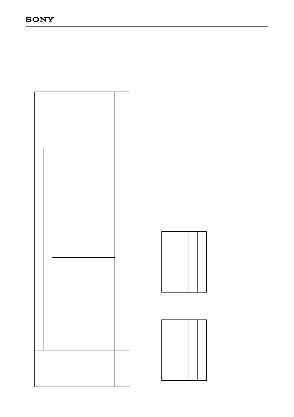
DATA (Pin 22) 8-bit transfer
D3
FS4
Focus
0
0
D6 D5 D4
ADDRESS
D7
0
0
Item
System Control
FOCUS
1 = ON
0 = OFF
TG1, TG2
CONTROL
1 = GAIN UP
0 = NORMAL
1
0
0
0
TRACKING
CONTROL
TRACKING MODE
0
1
0
0
TRACKING
SLED MODE
– 37 –
OFF
SLED MODE
ON
∗2
0
0
OFF
1
0
ON
D2
D3
TRACKING MODE
1
∗
FWD MOVE
REV MOVE
0
1
1
1
FWD JUMP
REV JUMP
Page 38
CXA1992R
SENS2
SENS1
D1 D0
DATA
BAL1
BAL2
BAL3
BALL
BALH
1 = OFF
0 = ON
1 = OFF
0 = ON
1 = OFF
0 = ON
TGL
TGH
TOG1
TOG2
TOG3
1 = OFF
0 = ON
1 = OFF
0 = ON
1 = OFF
0 = ON
IFB1
IFB2
IFB3
FOL
FOH
1 = OFF
0 = ON
1 = OFF
0 = ON
1 = OFF
0 = ON
H
ATSC
LPC
LPCL
LDON
(HIGH-Z)
1 = ON
0 = OFF
1 = ±30%
0 = ±10%
1 = ON
0 = OFF
BAL4
1 = OFF
0 = ON
TOG4
—
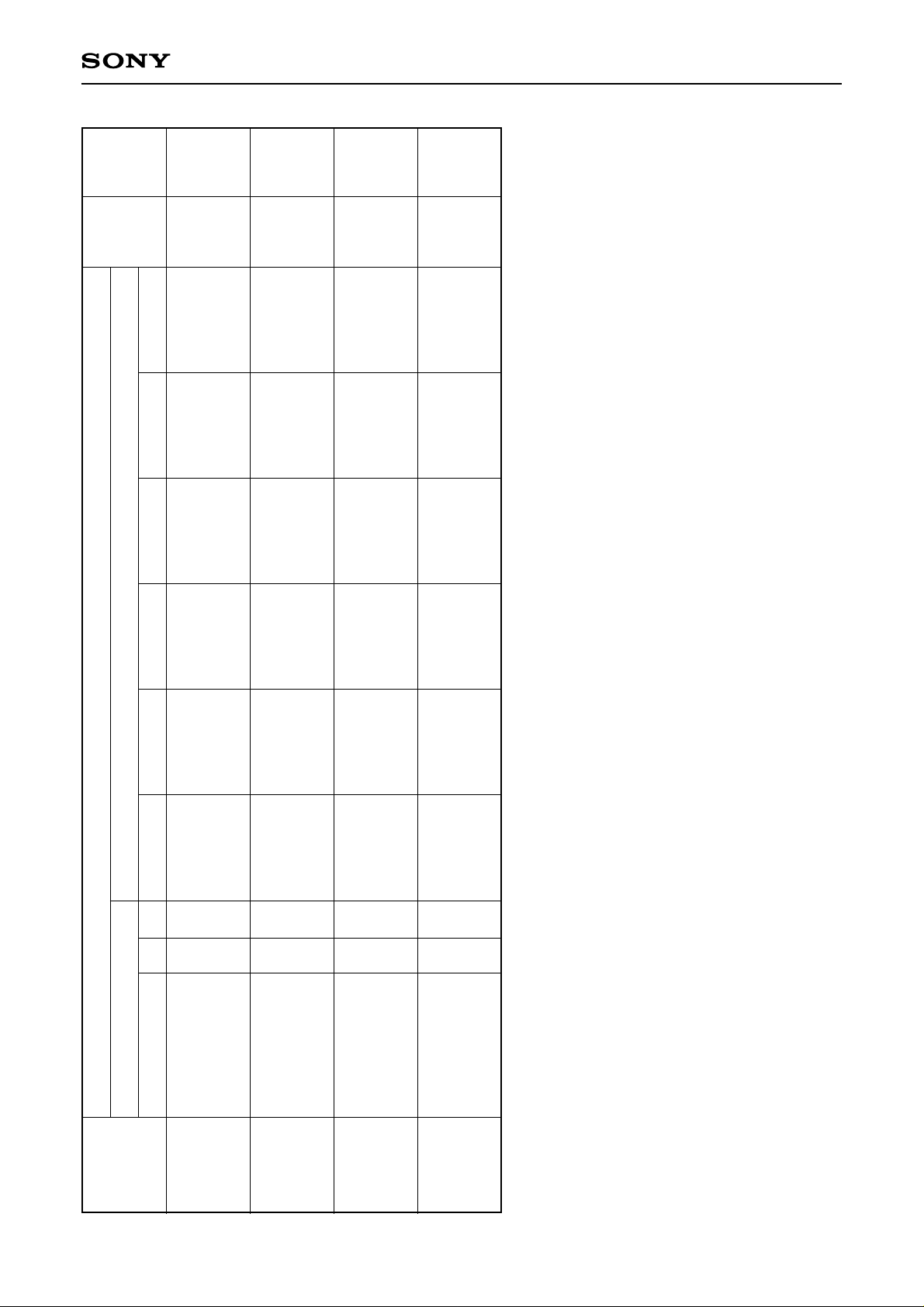
DATA (Pin 22) 12-bit transfer
D5 D4 D3 D2
DFCT
1 = DISABLE
0 = ENABLE
TGFL
0
D7 D6
0
1
1
ADDRESS
0
D11 D10 D9 D8
0
1 = OFF
0 = ON
IFB4
—
IFB5
1 = GAIN UP
0 = NORMAL
IFB6
1
0
1
1
0
0
1 = OFF
0 = ON
1 = OFF
0 = ON
1 = OFF
0 = ON
0
1
1
1
0
0
ATSC
1 = DISABLE
RDFCT2
1 = RESET
INT
1 = ENABLE
1
1
1
1
0
0
0 = ENABLE
0 = NORMAL
0 = DISABLE
Item
E-F
BALANCE
TRACKING
GAIN
FOCUS
BIAS
Others
– 38 –
Notes)
• When ATSC is enabled, even if TG1 and TG2 are NORMAL mode, TG1 and TG2 switch to GAIN UP mode in conjunction with ATSC and LOCK.
• INT is forcibly disabled regardless of the command when the tracking gain is increased. (including when the gain is increased by ATSC or LOCK)
When reset
• SENS1 = FZC
• SENS2 = High (Hi-Z)
• RDFCT2 = 1 (Reset)
• IFB1 to IFB6 = 0 (switch ON)
• TOG1 to TOG4 = 0 (switch ON)
• BAL1 to BAL4 = 1 (switch ON)
• Other data is "0".
Page 39
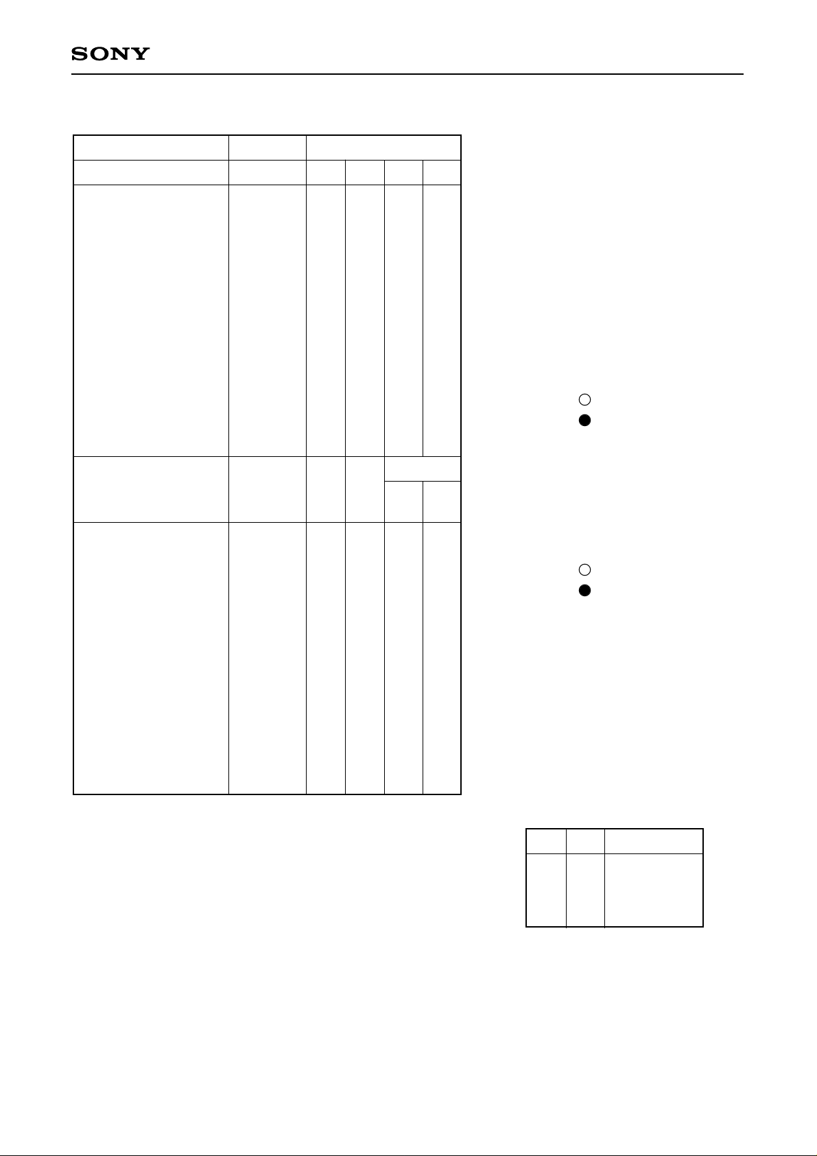
Serial Data Truth Table
CXA1992R
Serial Data
FOCUS CONTROL
0000 0000
0000 0001
0000 0010
0000 0011
0000 0100
0000 0101
0000 0110
0000 0111
0000 1000
0000 1001
0000 1010
0000 1011
0000 1100
0000 1101
0000 1110
0000 1111
TRACKING CONTROL
0001 0000
0001 0001
0001 0010
0001 0011
0001 0100
0001 0101
0001 0110
0001 0111
0001 1000
0001 1001
0001 1010
0001 1011
0001 1100
0001 1101
0001 1110
0001 1111
HEX Functions
$00
$01
$02
$03
$04
$05
$06
$07
$08
$09
$0A
$0B
$0C
$0D
$0E
$0F
$10
$11
$12
$13
$14
$15
$16
$17
$18
$19
$1A
$1B
$1C
$1D
$1E
$1F
FS4
0
0
0
0
0
0
0
0
1
1
1
1
1
1
1
1
TG1
TG2
0
0
0
0
0
0
0
0
1
1
1
1
1
1
1
1
BRAK
Fig. 6
D2
0
0
0
0
1
1
1
1
0
0
0
0
1
1
1
1
FS2 FS1
0
0
1
1
0
0
1
1
0
0
1
1
0
0
1
1
SLD KICK
KICK
+2
0
0
1
1
0
0
1
1
0
0
1
1
0
0
1
1
0
1
0
1
0
1
0
1
0
1
0
1
0
1
0
1
KICK
+1
0
1
0
1
0
1
0
1
0
1
0
1
0
1
0
1
Notes) • FS1
1: OFF
0: ON
• FS2
1: ON
0: OFF
• FS4
In the Block Diagram:
1:SW side
0:SW side
Notes) • TG1
In the Block Diagram:
1:SW side
0:SW side
• TG2
1: OFF
0: ON
• BRAKE
When D2 in Fig. 6 is:
1: 1
0: 0
– 39 –
• Sled kick height
D1
D0 Relative value
0
0
±1
0
1
±2
1
0
±3
1
1
±4
Page 40
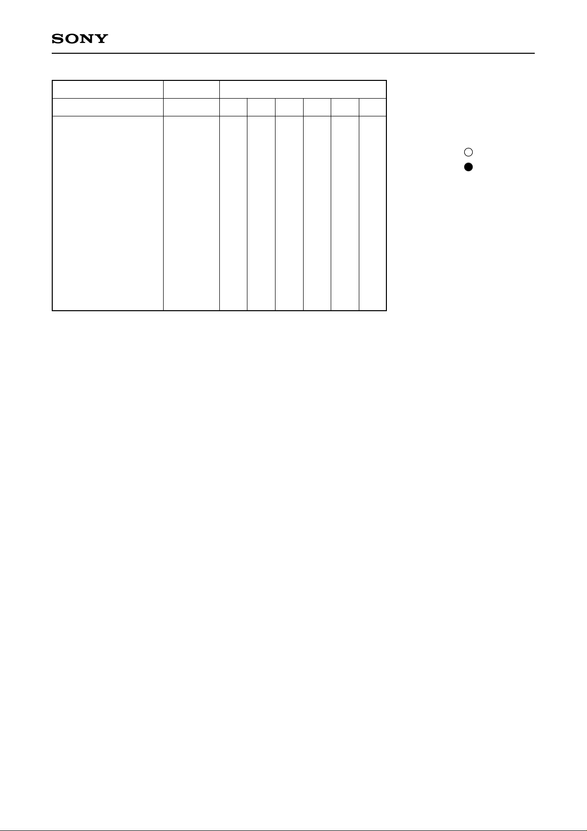
CXA1992R
Serial Data
TRACKING/SLED MODE
0010 0000
0010 0001
0010 0010
0010 0011
0010 0100
0010 0101
0010 0110
0010 0111
0010 1000
0010 1001
0010 1010
0010 1011
0010 1100
0010 1101
0010 1110
0010 1111
HEX Function
TM6 TM5 TM4 TM3
$20
$21
$22
$23
$24
$25
$26
$27
$28
$29
$2A
$2B
$2C
$2D
$2E
$2F
0
0
0
0
0
0
0
0
0
1
0
0
1
0
0
0
0
0
0
0
0
0
0
0
0
1
0
0
1
0
0
0
0
0
0
1
0
0
0
1
0
1
0
1
1
0
0
1
0
0
1
0
0
0
1
0
0
1
1
0
1
0
1
0
TM2
0
1
0
0
0
1
0
0
0
1
0
0
0
1
0
0
TM1
0
0
0
0
1
1
1
1
0
0
0
0
0
0
0
0
Notes) • TM1/TM2
In the Block Diagram:
1:SW side
0:SW side
• TM3/TM4/TM5/TM6
1: ON
0: OFF
– 40 –
Page 41
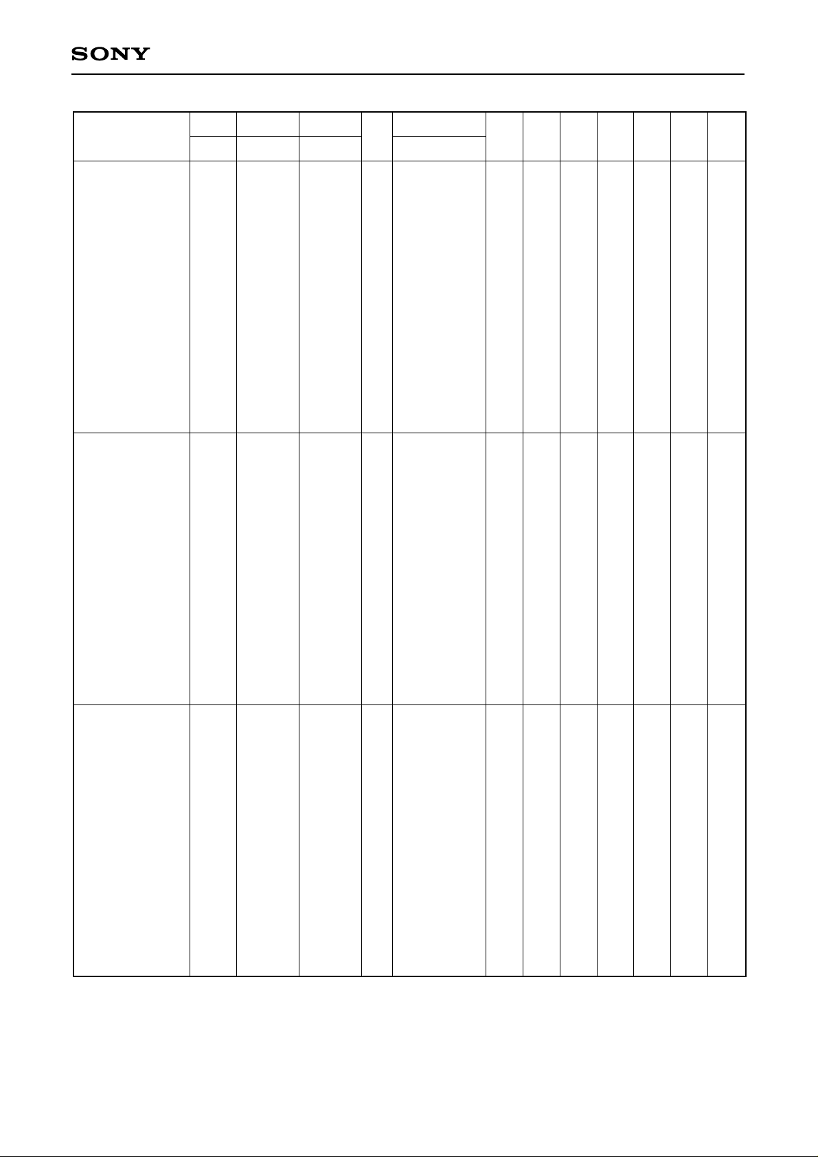
CXA1992R
Serial Data
$3XX
0011 0000 0000
0011 0000 0001
0011 0000 0010
0011 0000 0011
0011 0000 0100
0011 0000 0101
0011 0000 0110
0011 0000 0111
0011 0000 1000
0011 0000 1001
0011 0000 1010
0011 0000 1011
0011 0000 1100
0011 0000 1101
0011 0000 1110
0011 0000 1111
0011 0001 0000
0011 0001 0001
0011 0001 0010
0011 0001 0011
0011 0001 0100
0011 0001 0101
0011 0001 0110
0011 0001 0111
0011 0001 1000
0011 0001 1001
0011 0001 1010
0011 0001 1011
0011 0001 1100
0011 0001 1101
0011 0001 1110
0011 0001 1111
HEX BAL SW
43214321 456321
$300
$301
$302
$303
$304
$305
$306
$307
$308
$309
$30A
$30B
$30C
$30D
$30E
$30F
$310
$311
$312
$313
$314
$315
$316
$317
$318
$319
$31A
$31B
$31C
$31D
$31E
$31F
1
1
1
1
1
1
1
1
0
1
1
0
1
0
1
1
0
1
1
0
0
1
0
0
0
1
1
0
1
1
0
1
0
0
1
0
0
0
1
0
0
1
0
0
0
0
0
0
1
1
1
1
1
1
1
1
0
1
1
0
1
0
1
1
0
1
1
0
0
1
0
0
0
1
1
0
1
1
0
1
0
0
1
0
0
0
1
0
0
1
0
0
0
0
0
0
TOG SW IFB SW
TGFL
1
—
—
—
—
0
—
—
—
—
1
—
—
—
—
0
—
—
—
—
1
—
—
—
—
0
—
—
—
—
1
—
—
—
—
0
—
—
—
—
1
—
—
—
—
0
—
—
—
—
1
—
—
—
—
0
—
—
—
—
1
—
—
—
—
0
—
—
—
—
1
—
—
—
—
0
—
—
—
—
1
—
—
—
—
0
—
—
—
—
1
—
—
—
—
0
—
—
—
—
1
—
—
—
—
0
—
—
—
—
1
—
—
—
—
0
—
—
—
—
1
—
—
—
—
0
—
—
—
—
1
—
—
—
—
0
—
—
—
—
1
—
—
—
—
0
—
—
—
—
1
—
—
—
—
0
—
—
—
—
—
—
—
—
—
—
—
—
—
—
—
—
—
—
—
—
—
—
—
—
—
—
—
—
—
—
—
—
—
—
—
—
—
—
—
—
—
—
—
—
—
—
—
—
—
—
—
—
—
—
—
—
—
—
—
—
—
—
—
—
—
—
—
—
—
—
—
—
—
—
—
—
—
—
—
—
—
—
—
—
—
—
—
—
—
—
—
—
—
—
—
—
—
—
—
—
—
—
—
—
—
—
—
—
—
—
—
—
—
—
—
—
—
—
—
—
—
—
—
—
—
—
—
—
—
—
—
—
—
—
—
—
—
—
—
—
—
—
—
—
—
—
—
—
—
—
—
—
—
—
—
—
—
—
—
—
—
—
—
—
—
—
—
—
—
—
—
—
—
—
—
—
—
—
—
—
—
—
—
—
—
—
—
—
—
—
—
—
—
—
—
—
—
—
—
—
—
—
—
—
—
—
—
—
—
—
—
—
—
—
—
—
—
—
—
—
—
—
—
—
—
—
—
—
INT
—
—
—
—
—
—
—
—
—
—
—
—
—
—
—
—
—
—
—
—
—
—
—
—
—
—
—
—
—
—
—
—
RDF
CT2
—
—
—
—
—
—
—
—
—
—
—
—
—
—
—
—
—
—
—
—
—
—
—
—
—
—
—
—
—
—
—
—
ATSC
—
—
—
—
—
—
—
—
—
—
—
—
—
—
—
—
—
—
—
—
—
—
—
—
—
—
—
—
—
—
—
—
LDON
—
—
—
—
—
—
—
—
—
—
—
—
—
—
—
—
—
—
—
—
—
—
—
—
—
—
—
—
—
—
—
—
LPCL LPC
—
—
—
—
—
—
—
—
—
—
—
—
—
—
—
—
—
—
—
—
—
—
—
—
—
—
—
—
—
—
—
—
—
—
—
—
—
—
—
—
—
—
—
—
—
—
—
—
—
—
—
—
—
—
—
—
—
—
—
—
—
—
—
—
DFCT
E
E
E
E
E
E
E
E
E
E
E
E
E
E
E
E
E
E
E
E
E
E
E
E
E
E
E
E
E
E
E
E
0011 0010 0000
0011 0010 0001
0011 0010 0010
0011 0010 0011
0011 0010 0100
0011 0010 0101
0011 0010 0110
0011 0010 0111
0011 0010 1000
0011 0010 1001
0011 0010 1010
0011 0010 1011
0011 0010 1100
0011 0010 1101
0011 0010 1110
0011 0010 1111
$320
$321
$322
$323
$324
$325
$326
$327
$328
$329
$32A
$32B
$32C
$32D
$32E
$32F
1
1
1
1
—
—
—
—
1
1
1
0
—
—
—
—
1
1
0
1
—
—
—
—
1
1
0
0
—
—
—
—
1
0
1
1
—
—
—
—
1
0
1
0
—
—
—
—
1
0
0
1
—
—
—
—
1
0
0
0
—
—
—
—
0
1
1
1
—
—
—
—
0
1
1
0
—
—
—
—
0
1
0
1
—
—
—
—
0
1
0
0
—
—
—
—
0
0
1
1
—
—
—
—
0
0
1
0
—
—
—
—
0
0
0
1
—
—
—
—
0
0
0
0
—
—
—
—
—
—
—
—
—
—
—
—
—
—
—
—
—
—
—
—
—
—
—
—
—
—
—
—
—
—
—
—
—
—
—
—
—
—
—
—
—
—
—
—
—
—
—
—
—
—
—
—
—
—
—
—
—
—
—
—
—
—
—
—
—
—
—
—
—
—
—
—
—
—
—
—
—
—
—
—
—
—
—
—
—
—
—
—
—
—
—
—
—
—
—
—
—
—
—
—
—
—
—
—
—
—
—
—
—
—
—
—
—
—
—
—
—
—
—
—
—
—
—
—
—
—
—
—
—
—
—
—
—
—
—
—
—
—
—
—
—
—
—
—
—
—
—
—
—
—
—
—
—
—
—
—
—
—
—
—
—
—
—
—
—
—
—
—
—
—
—
—
—
—
—
—
—
—
—
—
—
—
—
—
—
—
—
—
—
—
—
—
—
—
—
—
—
—
—
—
—
—
—
—
—
—
—
—
—
—
—
—
D
D
D
D
D
D
D
D
D
D
D
D
D
D
D
D
– 41 –
Page 42
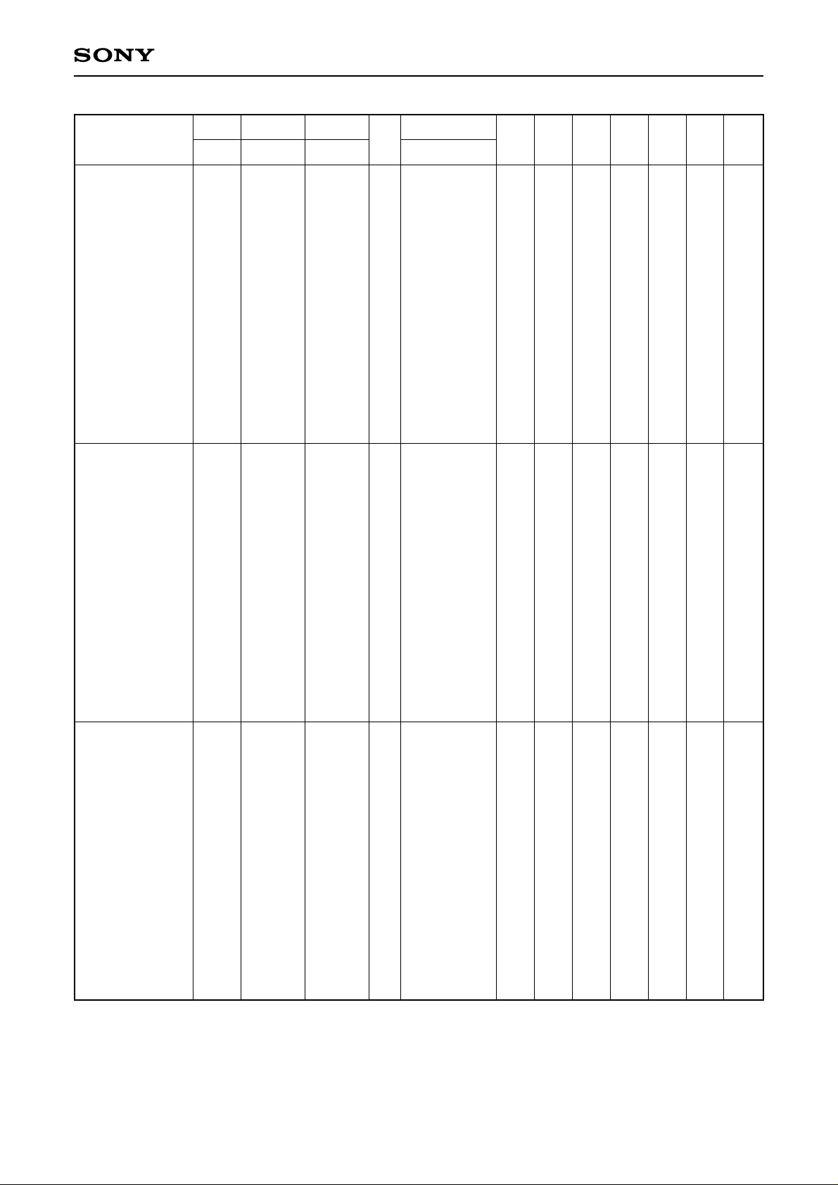
CXA1992R
Serial Data
$3XX
0011 0011 0000
0011 0011 0001
0011 0011 0010
0011 0011 0011
0011 0011 0100
0011 0011 0101
0011 0011 0110
0011 0011 0111
0011 0011 1000
0011 0011 1001
0011 0011 1010
0011 0011 1011
0011 0011 1100
0011 0011 1101
0011 0011 1110
0011 0011 1111
0011 0100 0000
0011 0100 0001
0011 0100 0010
0011 0100 0011
0011 0100 0100
0011 0100 0101
0011 0100 0110
0011 0100 0111
0011 0100 1000
0011 0100 1001
0011 0100 1010
0011 0100 1011
0011 0100 1100
0011 0100 1101
0011 0100 1110
0011 0100 1111
HEX BAL SW
43214321 456 321
$330
$331
$332
$333
$334
$335
$336
$337
$338
$339
$33A
$33B
$33C
$33D
$33E
$33F
$340
$341
$342
$343
$344
$345
$346
$347
$348
$349
$34A
$34B
$34C
$34D
$34E
$34F
1
1
1
1
1
1
1
1
0
0
0
0
0
0
0
0
—
—
—
—
—
—
—
—
—
—
—
—
—
—
—
—
1
1
1
1
0
0
0
0
1
1
1
1
0
0
0
0
—
—
—
—
—
—
—
—
—
—
—
—
—
—
—
—
1
1
0
0
1
1
0
0
1
1
0
0
1
1
0
0
—
—
—
—
—
—
—
—
—
—
—
—
—
—
—
—
TOG SW IFB SW
TGFL
1
—
—
—
—
—
—
—
—
—
—
—
—
—
—
—
—
—
—
—
—
0
—
—
—
—
1
—
—
—
—
0
—
—
—
—
1
—
—
—
—
0
—
—
—
—
1
—
—
—
—
0
—
—
—
—
1
—
—
—
—
0
—
—
—
—
1
—
—
—
—
0
—
—
—
—
1
—
—
—
—
0
—
—
—
—
1
—
—
—
—
0
—
—
—
—
1
1
1
1
1
1
1
0
1
1
0
1
1
1
0
0
1
0
1
1
1
0
1
0
1
0
0
1
1
0
0
0
0
1
1
1
0
1
1
0
0
1
0
1
0
1
0
0
0
0
1
1
0
0
1
0
0
0
0
1
0
0
0
0
—
—
—
—
—
—
—
—
—
—
—
—
—
—
—
—
0
0
0
0
0
0
0
0
0
0
0
0
0
0
0
0
—
—
—
—
—
—
—
—
—
—
—
—
—
—
—
—
—
—
—
—
—
—
—
—
—
—
—
—
—
—
—
—
—
—
—
—
—
—
—
—
—
—
—
—
—
—
—
—
—
—
—
—
—
—
—
—
—
—
—
—
—
—
—
—
—
—
—
—
—
—
—
—
—
—
—
—
—
—
—
—
—
—
—
—
—
—
—
—
—
—
—
—
—
—
—
—
—
—
—
—
—
—
—
—
—
—
—
—
—
—
—
—
—
—
—
—
—
—
—
—
—
—
—
—
—
—
—
—
—
—
—
—
—
—
—
—
—
—
—
—
—
—
—
—
—
—
—
—
—
—
—
—
—
—
—
—
—
—
—
—
—
—
—
—
—
—
—
—
—
—
—
—
—
—
—
—
—
—
—
—
—
—
—
—
—
—
—
—
—
—
—
—
INT
—
—
—
—
—
—
—
—
—
—
—
—
—
—
—
—
—
—
—
—
—
—
—
—
—
—
—
—
—
—
—
—
RDF
CT2
—
—
—
—
—
—
—
—
—
—
—
—
—
—
—
—
—
—
—
—
—
—
—
—
—
—
—
—
—
—
—
—
ATSC
—
—
—
—
—
—
—
—
—
—
—
—
—
—
—
—
—
—
—
—
—
—
—
—
—
—
—
—
—
—
—
—
LDON
—
—
—
—
—
—
—
—
—
—
—
—
—
—
—
—
—
—
—
—
—
—
—
—
—
—
—
—
—
—
—
—
LPCL LPC
—
—
—
—
—
—
—
—
—
—
—
—
—
—
—
—
—
—
—
—
—
—
—
—
—
—
—
—
—
—
—
—
—
—
—
—
—
—
—
—
—
—
—
—
—
—
—
—
—
—
—
—
—
—
—
—
—
—
—
—
—
—
—
—
DFCT
D
D
D
D
D
D
D
D
D
D
D
D
D
D
D
D
—
—
—
—
—
—
—
—
—
—
—
—
—
—
—
—
0011 0101 0000
0011 0101 0001
0011 0101 0010
0011 0101 0011
0011 0101 0100
0011 0101 0101
0011 0101 0110
0011 0101 0111
0011 0101 1000
0011 0101 1001
0011 0101 1010
0011 0101 1011
0011 0101 1100
0011 0101 1101
0011 0101 1110
0011 0101 1111
$350
$351
$352
$353
$354
$355
$356
$357
$358
$359
$35A
$35B
$35C
$35D
$35E
$35F
—
—
—
—
—
—
—
—
—
—
—
—
—
—
—
—
—
—
—
—
—
—
—
—
—
—
—
—
—
—
—
—
—
—
—
—
—
—
—
—
—
—
—
—
—
—
—
—
—
—
—
—
—
—
—
—
—
—
—
—
—
—
—
—
1
1
1
1
1
1
1
0
1
1
0
1
1
1
0
0
1
0
1
1
1
0
1
0
1
0
0
1
1
0
0
0
0
1
1
1
0
1
1
0
0
1
0
1
0
1
0
0
0
0
1
1
0
0
1
0
0
0
0
1
0
0
0
0
—
—
—
—
—
—
—
—
—
—
—
—
—
—
—
—
—
—
—
—
—
—
—
—
—
—
—
—
—
—
—
—
—
—
—
—
—
—
—
—
—
—
—
0
—
—
—
—
—
—
—
—
—
—
—
—
—
—
—
—
—
—
—
—
—
—
—
—
—
—
—
—
—
—
—
—
—
—
—
—
—
—
—
0
—
—
—
—
—
—
—
—
—
—
—
—
—
—
—
—
—
—
—
—
—
—
—
—
—
—
—
—
—
—
—
—
—
—
—
0
—
—
—
—
—
—
—
—
—
—
—
—
—
—
—
—
—
—
—
—
—
—
—
—
—
—
—
—
—
—
—
0
—
—
—
—
—
—
—
—
—
—
—
—
—
—
—
—
—
—
—
—
—
—
—
—
—
—
—
—
—
—
—
—
—
—
—
—
—
—
0
—
—
0
—
—
0
—
—
0
—
—
0
—
—
0
—
—
0
—
—
0
—
—
0
—
—
0
—
—
0
—
—
0
– 42 –
Page 43
CXA1992R
Serial Data
$3XX
0011 0110 0000
0011 0110 0001
0011 0110 0010
0011 0110 0011
0011 0110 0100
0011 0110 0101
0011 0110 0110
0011 0110 0111
0011 0110 1000
0011 0110 1001
0011 0110 1010
0011 0110 1011
0011 0110 1100
0011 0110 1101
0011 0110 1110
0011 0110 1111
0011 0111 0000
0011 0111 0001
0011 0111 0010
0011 0111 0011
0011 0111 0100
0011 0111 0101
0011 0111 0110
0011 0111 0111
0011 0111 1000
0011 0111 1001
0011 0111 1010
0011 0111 1011
0011 0111 1100
0011 0111 1101
0011 0111 1110
0011 0111 1111
HEX BAL SW
43214321 456321
$360
—
—
—
$361
—
—
—
$362
—
—
—
$363
—
—
—
$364
—
—
—
$365
—
—
—
$366
—
—
—
$367
—
—
—
$368
—
—
—
$369
—
—
—
$36A
—
—
—
$36B
—
—
—
$36C
$36D
$37C
$37D
$36E
$36F
$370
$371
$372
$373
$374
$375
$376
$377
$378
$379
$37A
$37B
$37E
$37F
—
—
—
—
—
—
—
—
—
—
—
—
—
—
—
—
—
—
—
—
—
—
—
—
—
—
—
—
—
—
—
—
—
—
—
—
—
—
—
—
—
—
—
—
—
—
—
—
—
—
—
—
—
—
—
—
—
—
—
—
TOG SW IFB SW
TGFL
—
1
1
1
—
—
—
—
—
—
—
—
—
—
—
—
—
—
—
—
—
—
—
—
—
—
—
—
—
—
—
—
—
—
—
1
1
1
1
0
1
1
0
1
1
1
0
0
1
0
1
1
1
0
1
0
1
0
0
1
1
0
0
0
0
1
1
1
0
1
1
0
0
1
0
1
0
1
0
0
0
0
1
1
0
0
1
0
0
0
0
1
0
0
0
0
1
1
1
1
1
1
1
0
1
1
0
1
1
1
0
0
1
0
1
1
1
0
1
0
1
0
0
1
1
0
0
0
0
1
1
1
0
1
1
0
0
1
0
1
0
1
0
0
0
0
1
1
0
0
1
0
0
0
0
1
0
0
0
0
—
—
1
—
—
1
—
—
1
—
—
1
—
—
1
—
—
1
—
—
1
—
—
1
—
—
1
—
—
1
—
—
1
—
—
1
—
—
1
—
—
1
—
—
1
—
—
1
—
—
1
—
—
1
—
—
1
—
—
1
—
—
1
—
—
1
—
—
1
—
—
1
—
—
1
—
—
1
—
—
1
—
—
1
—
—
1
—
—
1
—
—
1
—
—
1
—
—
—
—
—
—
—
—
—
—
—
—
—
—
—
—
—
—
—
—
—
—
—
—
—
—
—
—
—
—
—
—
—
—
—
—
—
—
—
—
—
—
—
—
—
—
—
—
—
—
—
—
—
—
—
—
—
—
—
—
—
—
—
—
—
—
—
—
—
—
—
—
—
—
—
—
—
—
—
—
—
—
—
—
—
—
—
—
—
—
—
—
—
—
—
—
—
—
—
—
—
—
—
—
—
—
—
—
—
—
—
—
—
—
—
—
—
—
—
—
—
—
—
—
—
—
—
—
INT
—
—
—
—
—
—
—
—
—
—
—
—
—
—
—
—
—
—
—
—
—
—
—
—
—
—
—
—
—
—
—
—
RDF
CT2
—
—
—
—
—
—
—
—
—
—
—
—
—
—
—
—
—
—
—
—
—
—
—
—
—
—
—
—
—
—
—
—
ATSC
—
—
—
—
—
—
—
—
—
—
—
—
—
—
—
—
—
—
—
—
—
—
—
—
—
—
—
—
—
—
—
—
LDON
—
—
—
—
—
—
—
—
—
—
—
—
—
—
—
—
—
—
—
—
—
—
—
—
—
—
—
—
—
—
—
—
LPCL LPC
—
—
—
—
—
—
—
—
—
—
—
—
—
—
—
—
—
—
—
—
—
—
—
—
—
—
—
—
—
—
—
—
—
—
—
—
—
—
—
—
—
—
—
—
—
—
—
—
—
—
—
—
—
—
—
—
—
—
—
—
—
—
—
—
DFCT
—
—
—
—
—
—
—
—
—
—
—
—
—
—
—
—
—
—
—
—
—
—
—
—
—
—
—
—
—
—
—
—
0011 1000 0000
0011 1000 0001
0011 1000 0010
0011 1000 0011
0011 1000 0100
0011 1000 0101
0011 1000 0110
0011 1000 0111
0011 1000 1000
0011 1000 1001
0011 1000 1010
0011 1000 1011
0011 1000 1100
0011 1000 1101
0011 1000 1110
0011 1000 1111
$380
$381
$382
$383
$384
$385
$386
$387
$388
$389
$38A
$38B
$38C
$38D
$38E
$38F
—
—
—
—
—
—
—
—
—
—
—
—
—
—
—
—
—
—
—
—
—
—
—
—
—
—
—
—
—
—
—
—
—
—
—
—
—
—
—
—
—
—
—
—
—
—
—
—
—
—
—
—
—
—
—
—
—
—
—
—
—
—
—
—
—
—
—
—
—
—
—
—
—
—
—
—
—
—
—
—
—
—
—
—
—
—
—
—
—
—
—
—
—
—
—
—
—
—
—
—
—
—
—
—
—
—
—
—
—
—
—
—
—
—
—
—
—
—
—
—
—
—
—
—
—
—
—
—
—
—
—
—
—
—
—
—
—
—
—
—
—
—
—
—
1
1
1
1
1
1
1
1
1
1
1
1
1
1
1
1
1
1
1
1
1
1
1
1
1
1
1
1
1
1
1
1
– 43 –
1
1
1
1
—
—
—
—
—
—
—
1
1
1
0
—
—
—
—
—
—
—
1
1
0
1
—
—
—
—
—
—
—
1
1
0
0
—
—
—
—
—
—
—
1
0
1
1
—
—
—
—
—
—
—
1
0
1
0
—
—
—
—
—
—
—
1
0
0
1
—
—
—
—
—
—
—
1
0
0
0
—
—
—
—
—
—
—
0
1
1
1
—
—
—
—
—
—
—
0
1
1
0
—
—
—
—
—
—
—
0
1
0
1
—
—
—
—
—
—
—
0
1
0
0
—
—
—
—
—
—
—
0
0
1
1
—
—
—
—
—
—
—
0
0
1
0
—
—
—
—
—
—
—
0
0
0
1
—
—
—
—
—
—
—
0
0
0
0
—
—
—
—
—
—
—
Page 44
CXA1992R
Serial Data
$3XX
0011 1001 0000
0011 1001 0001
0011 1001 0010
0011 1001 0011
0011 1001 0100
0011 1001 0101
0011 1001 0110
0011 1001 0111
0011 1001 1000
0011 1001 1001
0011 1001 1010
0011 1001 1011
0011 1001 1100
0011 1001 1101
0011 1001 1110
0011 1001 1111
0011 1010 0000
0011 1010 0001
0011 1010 0010
0011 1010 0011
0011 1010 0100
0011 1010 0101
0011 1010 0110
0011 1010 0111
0011 1010 1000
0011 1010 1001
0011 1010 1010
0011 1010 1011
0011 1010 1100
0011 1010 1101
0011 1010 1110
0011 1010 1111
HEX BAL SW
43214321 456 321
$390
—
—
—
$391
—
—
—
$392
—
—
—
$393
—
—
—
$394
—
—
—
$395
—
—
—
$396
—
—
—
$397
—
—
—
$398
—
—
—
$399
—
—
—
$39A
$39B
$39C
$39D
$39E
$39F
$3A0
$3A1
$3A2
$3A3
$3A4
$3A5
$3A6
$3A7
$3A8
$3A9
$3AA
$3AB
$3AC
$3AD
$3AE
$3AF
—
—
—
—
—
—
—
—
—
—
—
—
—
—
—
—
—
—
—
—
—
—
—
—
—
—
—
—
—
—
—
—
—
—
—
—
—
—
—
—
—
—
—
—
—
—
—
—
—
—
—
—
—
—
—
—
—
—
—
—
—
—
—
—
—
—
TOG SW IFB SW
TGFL
—
—
—
—
—
—
—
—
—
—
—
—
—
—
—
—
—
—
—
—
—
—
—
—
—
—
—
—
—
—
—
—
—
—
—
—
—
—
—
—
—
—
—
—
—
—
—
—
—
—
—
—
—
—
—
—
—
—
—
—
—
—
—
—
—
—
—
—
—
—
—
—
—
—
—
—
—
—
—
—
—
—
—
—
—
—
—
—
—
—
—
—
—
—
—
—
—
—
—
—
—
—
—
—
—
—
—
—
—
—
—
—
—
—
—
—
—
—
—
—
—
—
—
—
—
—
—
—
—
—
—
—
—
—
—
—
—
—
—
—
—
—
—
—
—
—
—
—
—
—
—
—
—
—
—
—
—
—
—
—
—
—
—
—
—
—
—
—
—
—
—
—
—
—
—
—
—
—
—
—
—
—
—
—
—
—
—
—
—
—
—
—
1
0
1
0
1
0
1
0
1
0
1
0
1
0
1
0
1
0
1
0
1
0
1
0
1
0
1
0
1
0
1
0
0
1
0
1
0
1
0
1
0
1
0
1
0
1
0
1
0
1
0
1
0
1
0
1
0
1
0
1
0
1
0
1
RDF
INT
1
1
1
1
—
1
1
1
0
—
1
1
0
1
—
1
1
0
0
—
1
0
1
1
—
1
0
1
0
—
1
0
0
1
—
1
0
0
0
—
0
1
1
1
—
0
1
1
0
—
0
1
0
1
—
0
1
0
0
—
0
0
1
1
—
0
0
1
0
—
0
0
0
1
—
0
0
0
0
—
1
1
1
1
—
1
1
1
0
—
1
1
0
1
—
1
1
0
0
—
1
0
1
1
—
1
0
1
0
—
1
0
0
1
—
1
0
0
0
—
0
1
1
1
—
0
1
1
0
—
0
1
0
1
—
0
1
0
0
—
0
0
1
1
—
0
0
1
0
—
0
0
0
1
—
0
0
0
0
—
CT2
—
—
—
—
—
—
—
—
—
—
—
—
—
—
—
—
—
—
—
—
—
—
—
—
—
—
—
—
—
—
—
—
ATSC
—
—
—
—
—
—
—
—
—
—
—
—
—
—
—
—
—
—
—
—
—
—
—
—
—
—
—
—
—
—
—
—
LDON
—
—
—
—
—
—
—
—
—
—
—
—
—
—
—
—
—
—
—
—
—
—
—
—
—
—
—
—
—
—
—
—
LPCL LPC
—
—
—
—
—
—
—
—
—
—
—
—
—
—
—
—
—
—
—
—
—
—
—
—
—
—
—
—
—
—
—
—
—
—
—
—
—
—
—
—
—
—
—
—
—
—
—
—
—
—
—
—
—
—
—
—
—
—
—
—
—
—
—
—
DFCT
—
—
—
—
—
—
—
—
—
—
—
—
—
—
—
—
—
—
—
—
—
—
—
—
—
—
—
—
—
—
—
—
0011 1011 0000
0011 1011 0001
0011 1011 0010
0011 1011 0011
0011 1011 0100
0011 1011 0101
0011 1011 0110
0011 1011 0111
0011 1011 1000
0011 1011 1001
0011 1011 1010
0011 1011 1011
0011 1011 1100
0011 1011 1101
0011 1011 1110
0011 1011 1111
$3B0
$3B1
$3B2
$3B3
$3B4
$3B5
$3B6
$3B7
$3B8
$3B9
$3BA
$3BB
$3BC
$3BD
$3BE
$3BF
—
—
—
—
—
—
—
—
—
—
—
—
—
—
—
—
—
—
—
—
—
—
—
—
—
—
—
—
—
—
—
—
—
—
—
—
—
—
—
—
—
—
—
—
—
—
—
—
—
—
—
—
—
—
—
—
—
—
—
—
—
—
—
—
—
—
—
—
—
—
—
—
—
—
—
—
—
—
—
—
—
—
—
—
—
—
—
—
—
—
—
—
—
—
—
—
—
—
—
—
—
—
—
—
—
—
—
—
—
—
—
—
—
—
—
—
—
—
—
—
—
—
—
—
—
—
—
—
—
—
—
—
—
—
—
—
—
—
—
—
—
—
—
—
0
0
0
0
0
0
0
0
0
0
0
0
0
0
0
0
0
0
0
0
0
0
0
0
0
0
0
0
0
0
0
0
– 44 –
1
1
1
1
—
—
—
—
—
—
—
1
1
1
0
—
—
—
—
—
—
—
1
1
0
1
—
—
—
—
—
—
—
1
1
0
0
—
—
—
—
—
—
—
1
0
1
1
—
—
—
—
—
—
—
1
0
1
0
—
—
—
—
—
—
—
1
0
0
1
—
—
—
—
—
—
—
1
0
0
0
—
—
—
—
—
—
—
0
1
1
1
—
—
—
—
—
—
—
0
1
1
0
—
—
—
—
—
—
—
0
1
0
1
—
—
—
—
—
—
—
0
1
0
0
—
—
—
—
—
—
—
0
0
1
1
—
—
—
—
—
—
—
0
0
1
0
—
—
—
—
—
—
—
0
0
0
1
—
—
—
—
—
—
—
0
0
0
0
—
—
—
—
—
—
—
Page 45
CXA1992R
Serial Data
$3XX
0011 1100 0000
0011 1100 0001
0011 1100 0010
0011 1100 0011
0011 1100 0100
0011 1100 0101
0011 1100 0110
0011 1100 0111
0011 1100 1000
0011 1100 1001
0011 1100 1010
0011 1100 1011
0011 1100 1100
0011 1100 1101
0011 1100 1110
0011 1100 1111
0011 1101 0000
0011 1101 0001
0011 1101 0010
0011 1101 0011
0011 1101 0100
0011 1101 0101
0011 1101 0110
0011 1101 0111
0011 1101 1000
0011 1101 1001
0011 1101 1010
0011 1101 1011
0011 1101 1100
0011 1101 1101
0011 1101 1110
0011 1101 1111
HEX BAL SW
43214321 456321
$3C0
$3C1
$3C2
$3C3
$3C4
$3C5
$3C6
$3C7
$3C8
$3C9
$3CA
$3CB
$3CC
$3CD
$3CE
$3CF
$3D0
$3D1
$3D2
$3D3
$3D4
$3D5
$3D6
$3D7
$3D8
$3D9
$3DA
$3DB
$3DC
$3DD
$3DE
$3DF
—
—
—
—
—
—
—
—
—
—
—
—
—
—
—
—
—
—
—
—
—
—
—
—
—
—
—
—
—
—
—
—
—
—
—
—
—
—
—
—
—
—
—
—
—
—
—
—
—
—
—
—
—
—
—
—
—
—
—
—
—
—
—
—
—
—
—
—
—
—
—
—
—
—
—
—
—
—
—
—
—
—
—
—
—
—
—
—
—
—
—
—
—
—
—
—
TOG SW IFB SW
TGFL
—
—
—
—
—
—
—
—
—
—
—
—
—
—
—
—
—
—
—
—
—
—
—
—
—
—
—
—
—
—
—
—
—
—
—
—
—
—
—
—
—
—
—
—
—
—
—
—
—
—
—
—
—
—
—
—
—
—
—
—
—
—
—
—
—
—
—
—
—
—
—
—
—
—
—
—
—
—
—
—
—
—
—
—
—
—
—
—
—
—
—
—
—
—
—
—
—
—
—
—
—
—
—
—
—
—
—
—
—
—
—
—
—
—
—
—
—
—
—
—
—
—
—
—
—
—
—
—
—
—
—
—
—
—
—
—
—
—
—
—
—
—
—
—
—
—
—
—
—
—
—
—
—
—
—
—
—
—
—
—
—
—
—
—
—
—
—
—
—
—
—
—
—
—
—
—
—
—
—
—
—
—
—
—
—
—
—
—
—
—
—
—
—
—
—
—
—
—
—
—
—
—
—
—
—
—
—
—
—
—
—
—
—
—
—
—
—
—
—
—
—
—
—
—
—
—
—
—
—
—
—
—
—
—
—
—
—
—
—
—
—
—
—
—
—
—
—
—
—
—
—
—
—
—
—
—
—
—
—
—
—
—
—
—
—
—
—
—
—
—
—
—
—
—
—
—
—
—
—
—
—
—
—
—
—
—
—
—
—
—
—
—
—
—
—
—
—
—
—
—
—
—
—
—
—
—
—
—
—
—
—
—
—
—
—
—
—
—
—
—
—
—
—
—
—
—
—
—
—
—
—
—
—
—
—
—
—
—
—
—
—
—
—
—
—
—
—
—
—
—
—
—
—
—
—
—
—
—
—
—
—
—
—
—
—
—
—
—
—
—
—
—
—
—
—
—
—
—
—
—
—
—
—
—
INT
0
0
0
0
0
0
0
0
0
0
0
0
0
0
0
0
0
0
0
0
0
0
0
0
0
0
0
0
0
0
0
0
RDF
CT2
0
0
0
0
0
0
0
0
0
0
0
0
0
0
0
0
1
1
1
1
1
1
1
1
1
1
1
1
1
1
1
1
ATSC
E
E
E
E
E
E
E
E
D
D
D
D
D
D
D
D
E
E
E
E
E
E
E
E
D
D
D
D
D
D
D
D
LDON
0
0
0
0
1
1
1
1
0
0
0
0
1
1
1
1
0
0
0
0
1
1
1
1
0
0
0
0
1
1
1
1
LPCL LPC
0
0
0
1
1
0
1
1
0
0
0
1
1
0
1
1
0
0
0
1
1
0
1
1
0
0
0
1
1
0
1
1
0
0
0
1
1
0
1
1
0
0
0
1
1
0
1
1
0
0
0
1
1
0
1
1
0
0
0
1
1
0
1
1
DFCT
—
—
—
—
—
—
—
—
—
—
—
—
—
—
—
—
—
—
—
—
—
—
—
—
—
—
—
—
—
—
—
—
0011 1110 0000
0011 1110 0001
0011 1110 0010
0011 1110 0011
0011 1110 0100
0011 1110 0101
0011 1110 0110
0011 1110 0111
0011 1110 1000
0011 1110 1001
0011 1110 1010
0011 1110 1011
0011 1110 1100
0011 1110 1101
0011 1110 1110
0011 1110 1111
$3E0
$3E1
$3E2
$3E3
$3E4
$3E5
$3E6
$3E7
$3E8
$3E9
$3EA
$3EB
$3EC
$3ED
$3EE
$3EF
—
—
—
—
—
—
—
—
—
—
—
—
—
—
—
—
—
—
—
—
—
—
—
—
—
—
—
—
—
—
—
—
—
—
—
—
—
—
—
—
—
—
—
—
—
—
—
—
—
—
—
—
—
—
—
—
—
—
—
—
—
—
—
—
—
—
—
—
—
—
—
—
—
—
—
—
—
—
—
—
—
—
—
—
—
—
—
—
—
—
—
—
—
—
—
—
—
—
—
—
—
—
—
—
—
—
—
—
—
—
—
—
—
—
—
—
—
—
—
—
—
—
—
—
—
—
—
—
—
—
—
—
—
—
—
—
—
—
—
—
—
—
—
—
—
—
—
—
—
—
—
—
—
—
—
—
—
—
—
—
—
—
—
—
—
—
—
—
—
—
—
—
—
—
—
—
– 45 –
—
—
—
—
—
—
—
—
—
—
—
—
—
—
—
—
—
—
—
—
—
—
—
—
—
—
—
—
—
—
—
—
—
—
—
—
—
—
—
—
—
—
—
—
—
—
—
—
—
—
—
—
—
—
—
—
—
—
—
—
—
—
—
—
1
0
E
0
0
0
—
1
0
E
0
0
1
—
1
0
E
0
1
0
—
1
0
E
0
1
1
—
1
0
E
1
0
0
—
1
0
E
1
0
1
—
1
0
E
1
1
0
—
1
0
E
1
1
1
—
1
0
D
0
0
0
—
1
0
D
0
0
1
—
1
0
D
0
1
0
—
1
0
D
0
1
1
—
1
0
D
1
0
0
—
1
0
D
1
0
1
—
1
0
D
1
1
0
—
1
0
D
1
1
1
—
Page 46
CXA1992R
Serial Data
$3XX
0011 1111 0000
0011 1111 0001
0011 1111 0010
0011 1111 0011
0011 1111 0100
0011 1111 0101
0011 1111 0110
0011 1111 0111
0011 1111 1000
0011 1111 1001
0011 1111 1010
0011 1111 1011
0011 1111 1100
0011 1111 1101
0011 1111 1110
0011 1111 1111
HEX BAL SW
43214321 456 321
$3F0
$3F1
$3F2
$3F3
$3F4
$3F5
$3F6
$3F7
$3F8
$3F9
$3FA
$3FB
$3FC
$3FD
$3FE
$3FF
—
—
—
—
—
—
—
—
—
—
—
—
—
—
—
—
—
—
—
—
—
—
—
—
—
—
—
—
—
—
—
—
TOG SW IFB SW
TGFL
—
—
—
—
—
—
—
—
—
—
—
—
—
—
—
—
—
—
—
—
—
—
—
—
—
—
—
—
—
—
—
—
—
—
—
—
—
—
—
—
—
—
—
—
—
—
—
—
—
—
—
—
—
—
—
—
—
—
—
—
—
—
—
—
—
—
—
—
—
—
—
—
—
—
—
—
—
—
—
—
—
—
—
—
—
—
—
—
—
—
—
—
—
—
—
—
—
—
—
—
—
—
—
—
—
—
—
—
—
—
—
—
—
—
—
—
—
—
—
—
—
—
—
—
—
—
—
—
—
—
—
—
—
—
—
—
—
—
—
—
—
—
—
—
—
—
—
—
—
—
—
—
—
—
—
—
—
—
—
—
—
—
—
—
—
—
—
—
—
—
—
—
—
—
—
—
—
—
—
—
—
—
—
—
—
—
—
—
—
—
—
—
—
—
—
—
—
—
—
—
—
—
—
—
—
—
—
—
INT
1
1
1
1
1
1
1
1
1
1
1
1
1
1
1
1
RDF
CT2
1
1
1
1
1
1
1
1
1
1
1
1
1
1
1
1
ATSC
E
E
E
E
E
E
E
E
D
D
D
D
D
D
D
D
LDON
0
0
0
0
1
1
1
1
0
0
0
0
1
1
1
1
LPCL LPC
0
0
0
1
1
0
1
1
0
0
0
1
1
0
1
1
0
0
0
1
1
0
1
1
0
0
0
1
1
0
1
1
DFCT
—
—
—
—
—
—
—
—
—
—
—
—
—
—
—
—
Notes) • 0 means OFF and 1 means ON for TOG SW and BAL SW. These are not equal to the setting values
of each bit for serial data.
• "—" in the Truth Table indicates that the status does not change.
• TGFL
In the Block Diagram:
1:SW side
0:SW side
• ATSC E: enable/D: disable
• DFCT E: enable/D: disable
– 46 –
Page 47
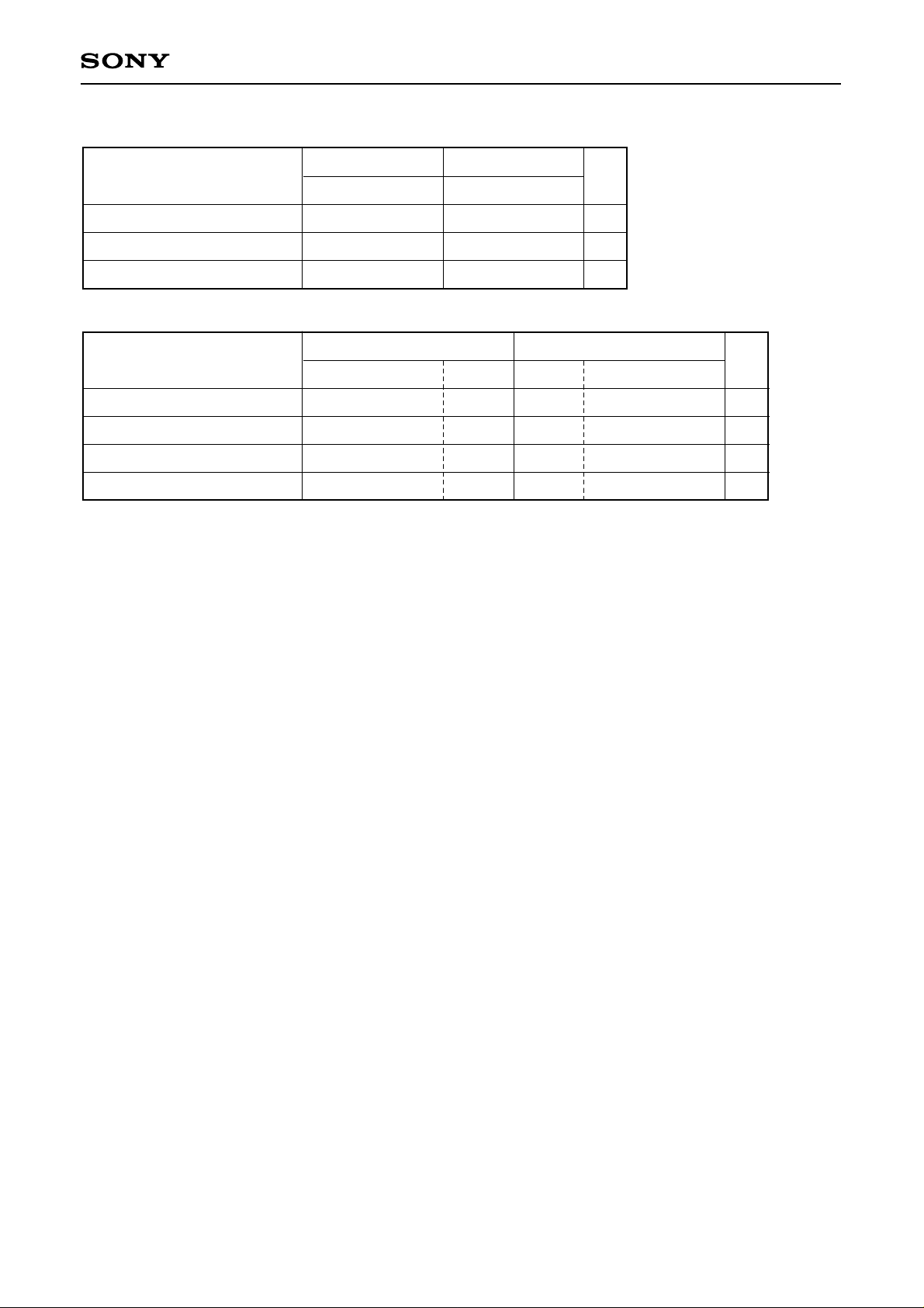
Initial State (resetting state)
CXA1992R
Item
FOCUS CONTROL
TRACKING CONTROL
TRACKING SLED MODE
Item
E-F BALANCE
TRACKING GAIN
FOCUS BIAS
Others
ADDRESS
D7
D6 D5 D4 D3 D2 D1 D0
0
0
0
0
0
0
0
1
0
0
1
0
ADDRESS
D11
D10 D9 D8 D7 D6 D5 D4
0
0
1
1
0
0
1
1
0
0
1
1
0
0
1
1
DATA
HEX
0
0
0
0
$00
0
0
0
0
$10
0
0
0
0
$20
DATA
HEX
D3
D2
D1
D0
0
0
0
0
0
0
0
0
1
0
0
0
0
0
1
0
0
0
0
0
0
1
1
0
1
0
0
0
$300
0
$340
0
$380
0
$3D0
0
The above data means the following operation modes.
FOCUS CONTROL : FOCUS OFF, FOCUS SEARCH OFF, FOCUS SEACH DOWN
TRACKING CONTROL : TG1-TG2 NORMAL, BRAKE DISABLE, SLED KICK relative height value ±1
TRACKING SLED MODE : TRACKING OFF, SLED OFF
E-F BALANCE : BAL1 to BAL4 = 0 (switch ON). DFCT ENABLE
TRACKING GAIN : TOG1 to TOG4 = 0 (switch ON), TGFL NORMAL
FOCUS BIAS : IFB1 to IFB6 = 0 (switch ON)
Others : INT DISABLE, DFCT2 RESET, ATSC ENABLE, LDON OFF, LPCL ±10%, LPC OFF
– 47 –
Page 48
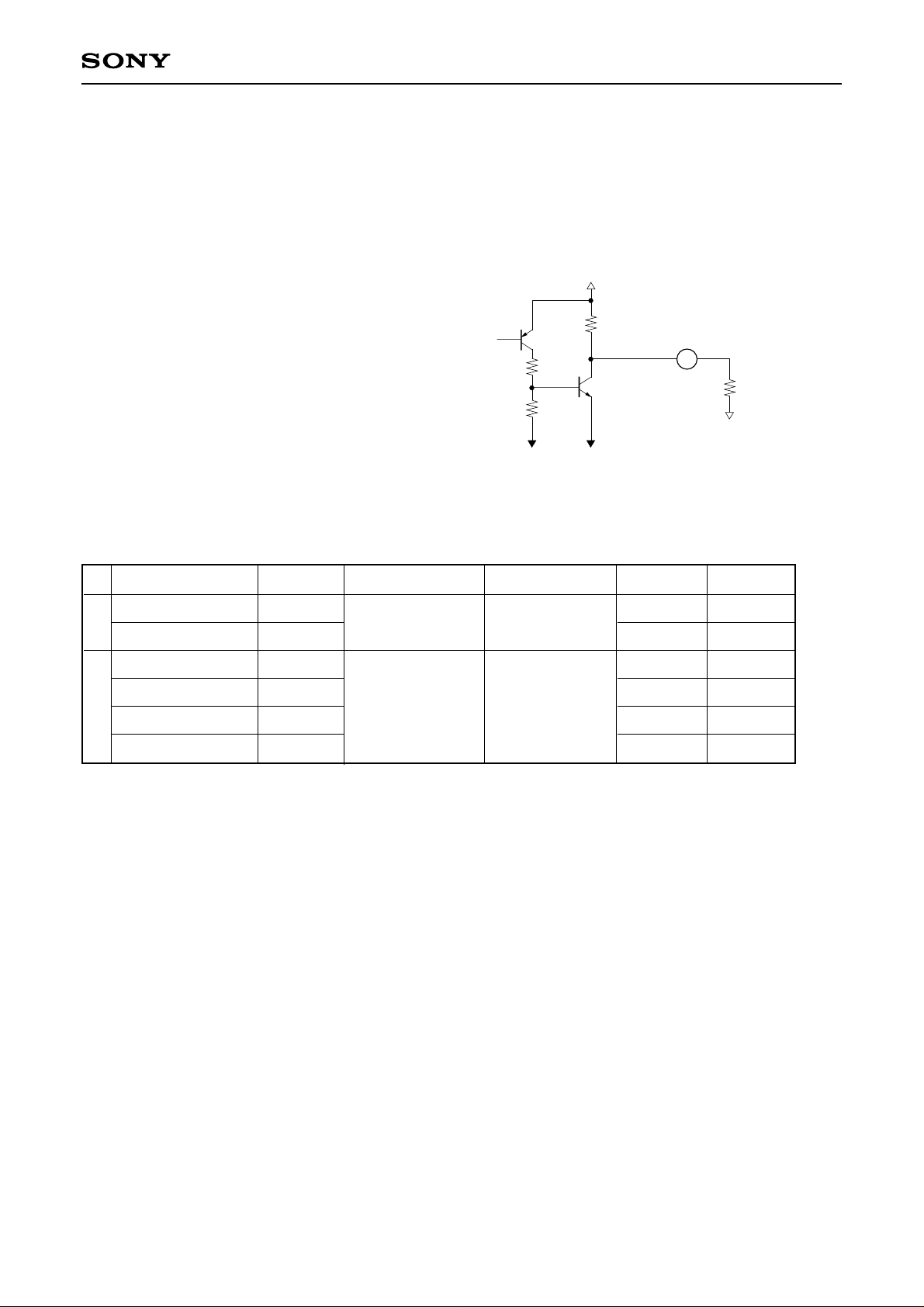
CXA1992R
Notes on Operation
1. Focus OK circuit
1) Refer to the "Description of Operation" for the time constant setting of the focus OK amplifier LPF and the
mirror amplifier HPF.
2) The equivalent circuit for the output pin (FOK) is shown in the diagram below.
VCC
The FOK and comparator output are as follows:
Output voltage High : VFOKH ≈ near Vcc
Output voltage Low : VFOKL ≈ Vsat (NPN) + VEE
20k
40k
100k
VEE VEE
FOK
27
RL
V
CC
2. Sled amplifier
The sled amplifier may oscillate when used by the buffer amplifier. Use with a gain of approximately 20dB.
3. Focus/Tracking internal phase compensation and reference design material
Item SD Measurement pin Conditions Typ. Unit
1.2kHz gain
FCS
1.2kHz phase
1.2kHz gain
1.2kHz phase
TRK
2.7kHz gain
2.7kHz phase
08
08
25
25
25 → 13
25 → 13
6
13
CFLB = 0.1µF
CFGD = 0.1µF
CTGU = 0.1µF
21.5
63
13
–125
26.5
–130
dB
deg
dB
deg
dB
deg
– 48 –
Page 49
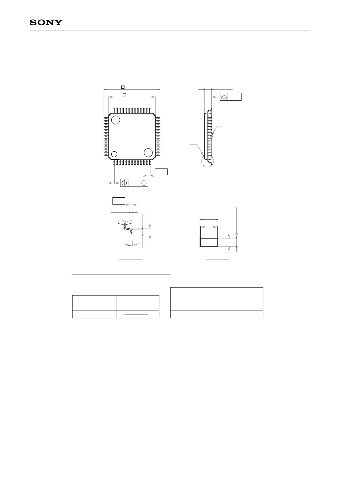
Package Outline Unit: mm
∗ 10.0 ± 0.1
39
12.0 ± 0.2
52PIN LQFP(PLASTIC)
27
+ 0.1
1.5 0
CXA1992R
0.1
40
52
1
+ 0.08
0.32 – 0.07
0.25
0.1 ± 0.1
0° to 10°
DETAIL
NOTE: “∗” Dimensions do not include mold protrusion.
SONY CODE
EIAJ CODE
JEDEC CODE
LQFP-52P-L01
LQFP052-P-1010
0.13
M
(11.0)
(0.5)
A
26
14
13
0.65
0.6 ± 0.15
B
A
+ 0.08
0.32 – 0.07
(0.3)
DETAIL
PACKAGE STRUCTURE
PACKAGE MATERIAL
LEAD TREATMENT
LEAD MATERIAL
PACKAGE MASS
EPOXY RESIN
PALLADIUM PLATING
COPPER ALLOY
0.3g
(0.125)
B
+ 0.04
0.145 – 0.025
– 49 –
 Loading...