

Page 1
CXA1917AM/AS
Dolby∗S type Noise Reduction Processor
Description
The CXA1917AM/AS is a bipolar IC designed for
use in the Dolby S type noise reduction system (NR).
An external operational amplifier is required to
configure the decoder. The stereo Dolby B-C-S type
NR combines use of a CXA1563M/S and two
CXA1917AM/AS ICs.
Features
• Considerable reduction in the number of external parts
(half compared to CXA1417S/Q)
• The same Dolby level as that of CXA1560 series ICs (–6dBm)
Structure
Bipolar silicon monolithic IC
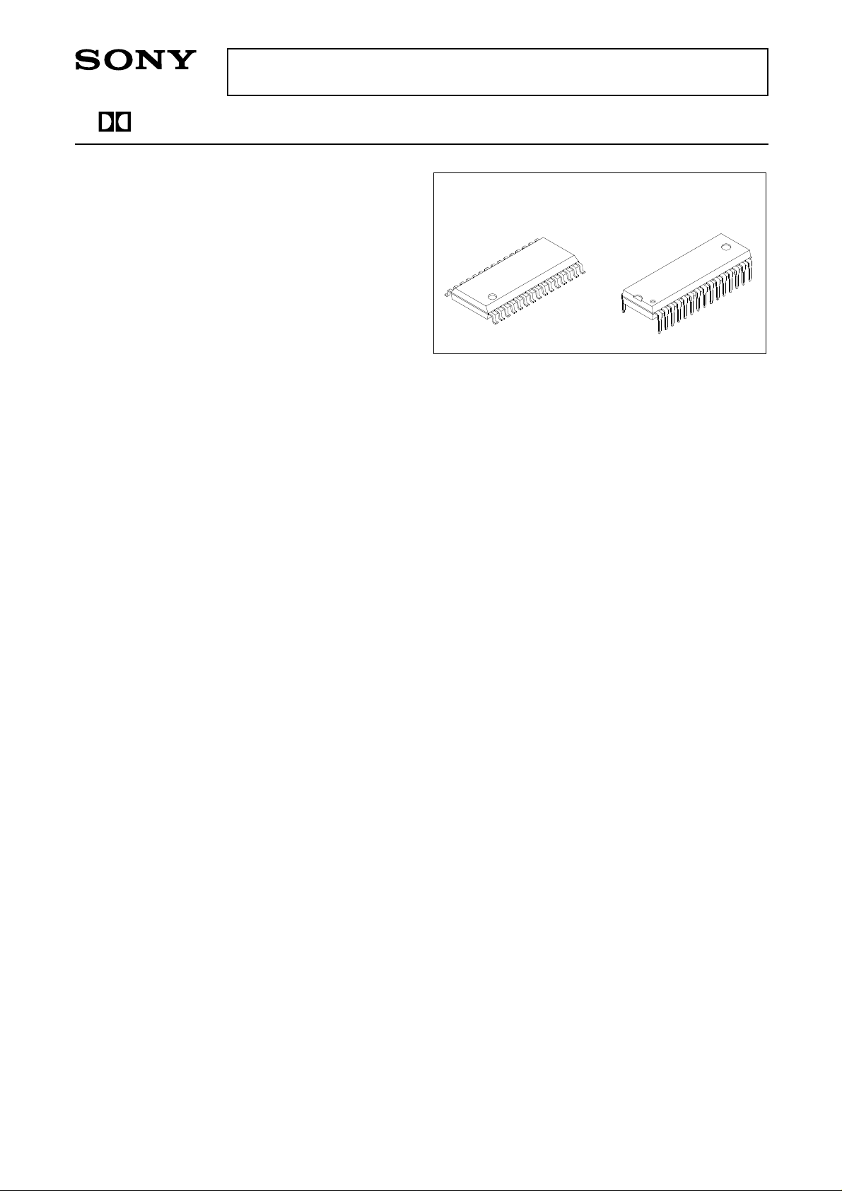
30 pin SOP (Plastic)
30 pin SDIP (Plastic)
Absolute Maximum Ratings (Ta = 25°C)
• Supply voltage VCC to VEE 17 V
• Operating temperature Topr –20 to +75 °C
• Storage temperature Tstg –65 to +150 °C
• Allowable power dissipation PD (CXA1917AM) 600 mW
(CXA1917AS) 1200 mW
Recommended Operating Conditions
Supply voltage VCC 4.5 to 6.5 V
VEE –4.5 to –6.5 V
∗
This IC is available only to the licensees of Dolby Laboratories Licensing Corporation from whom licensing and applications
information may be obtained.
∗
"Dolby" and the double D symbols are trademarks of Dolby Laboratories Licensing Corporation.
Sony reserves the right to change products and specifications without prior notice. This information does not convey any license by
any implication or otherwise under any patents or other right. Application circuits shown, if any, are typical examples illustrating the
operation of the devices. Sony cannot assume responsibility for any problems arising out of the use of these circuits.
– 1 –
E95Y15B74
Page 2
C45
R28
10%
0.47µ
C44
24k
R47
0.1µ
2%
33
16
17
18
19
CC
V
TCF2L IREF
CXA1917AM/AS
2
1
VCC
GND
VREF
VEE
&
IREF
4
3
VCT
14 15
C48
0.1µ
VCT
10%
13
C46
10%
47
0.22µ
R48
12
R27
10k
C25
2%
39n
VCT
C30
R30
2.2n
8.2k
C42
2%
10%
0.22µ
C40
C34
R34
R31
C29
R45
47n
8.2n
1.5k
13k
470p
C38
1µ
47
2%
20
21
22
23
24
25
26
27
TCS2L TCF1L
FBOL TCS1L
SCBOL
SLDET SLICG
ANTSAT
FLVCR SLVCR
20k
FLDET FLICG
V to I
Conv H
17.5k
15k
SHICG
SHDET
SHVCRFHVCR
LFDET
FHDET FHICG
V to I
Conv H
LFVCR LFICG
11
10
9
8
7
6
5
4
R26
R19
33
R46
C41
C31
C27
18k 2%
R25 33
39k 2%
C7
C43
10%
0.47µ
0.1µ
8.2n
680p
10k 2%
R24
C24 39n
10%
C23 0.22µ
C20 22n
R16 39k 2%
C17 100n
100n
Tolerances of resistors are 5% without otherwise specified
Tolerances of film capacitors are 5% without otherwise specified
Tolerances of chemical capacitors are 20% without otherwise specified
Single Supply: Short GND to VEE and open VCT
Note) Split Supply: Short VCT to GND
VCT
C26 1µ
VCT
28
C14
R12
10k
C8
100n
22n
29
20k
MC4IN MC3IN MCBO HLSOUT ZHSL RECOUT SCINL
MC4
MC3DS
MC4
MC2
MC1
MC3DT
MC
MC3
MC1
30
VCT
R9
39k
5
RECOUT
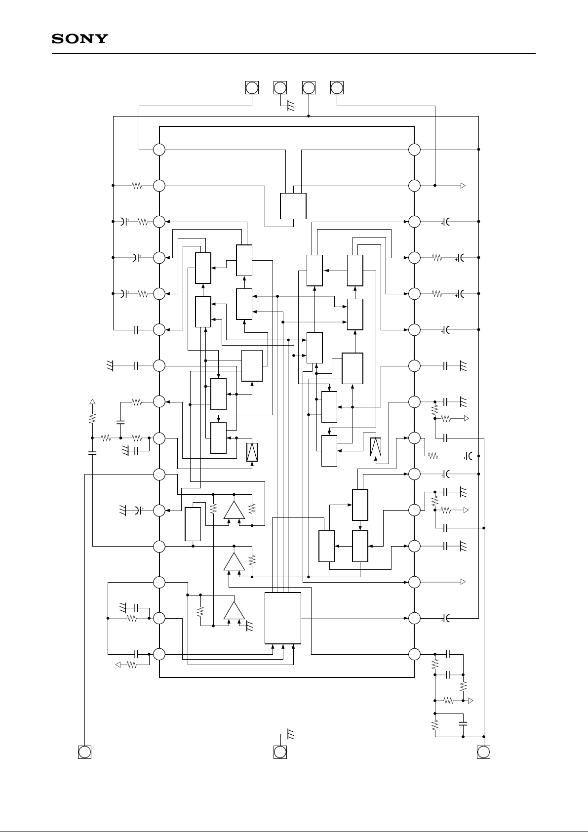
Block Diagram and Pin Configuration (Encoder Unit)
GND
6
– 2 –
3
C16
VCT
0.22µ
2
C21
5.1k 2%
C19
2%
1.8n
R15
1.8n
R14 16k 2%
C11
INPUT
2.4k 2%
VCT
100n
7
HLSMP MCTC ZHSH ZL2 LFIN TCL1 TCL2 SCINH FBOH TCF1H TCF2H TCS2H TCS1H VCT VEE
1
R20
27k
R10
Page 3

CXA1917AM/AS
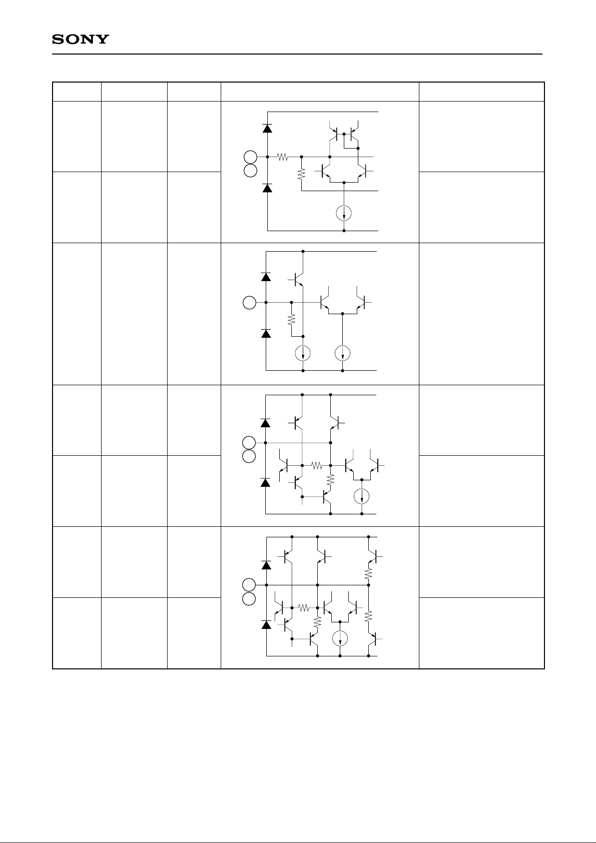
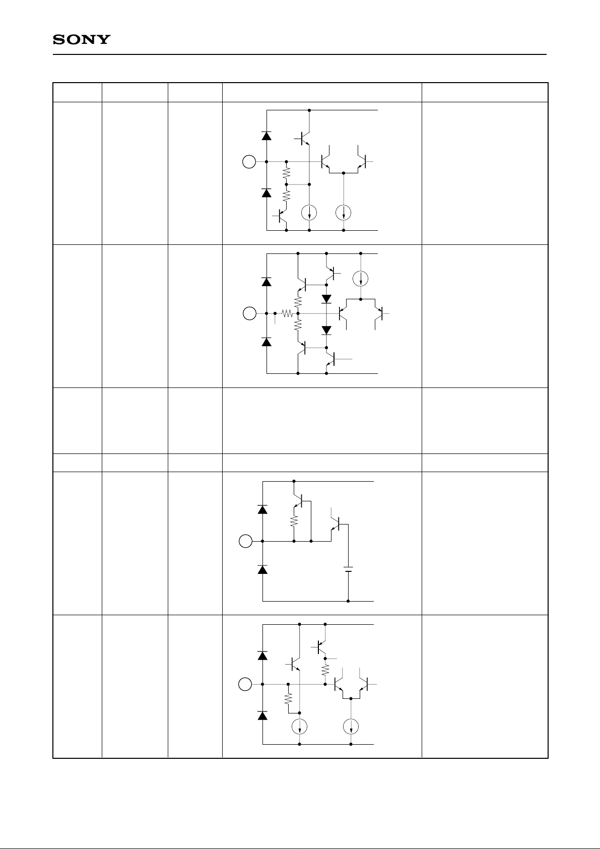
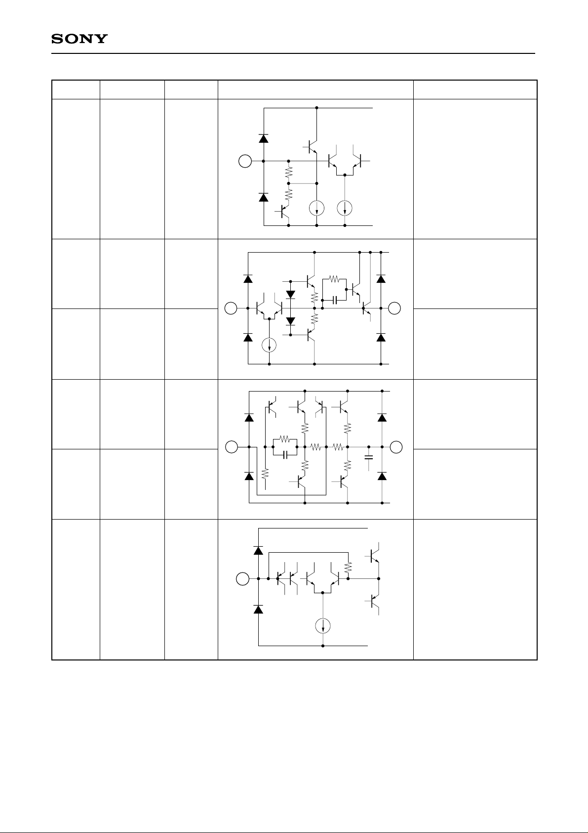
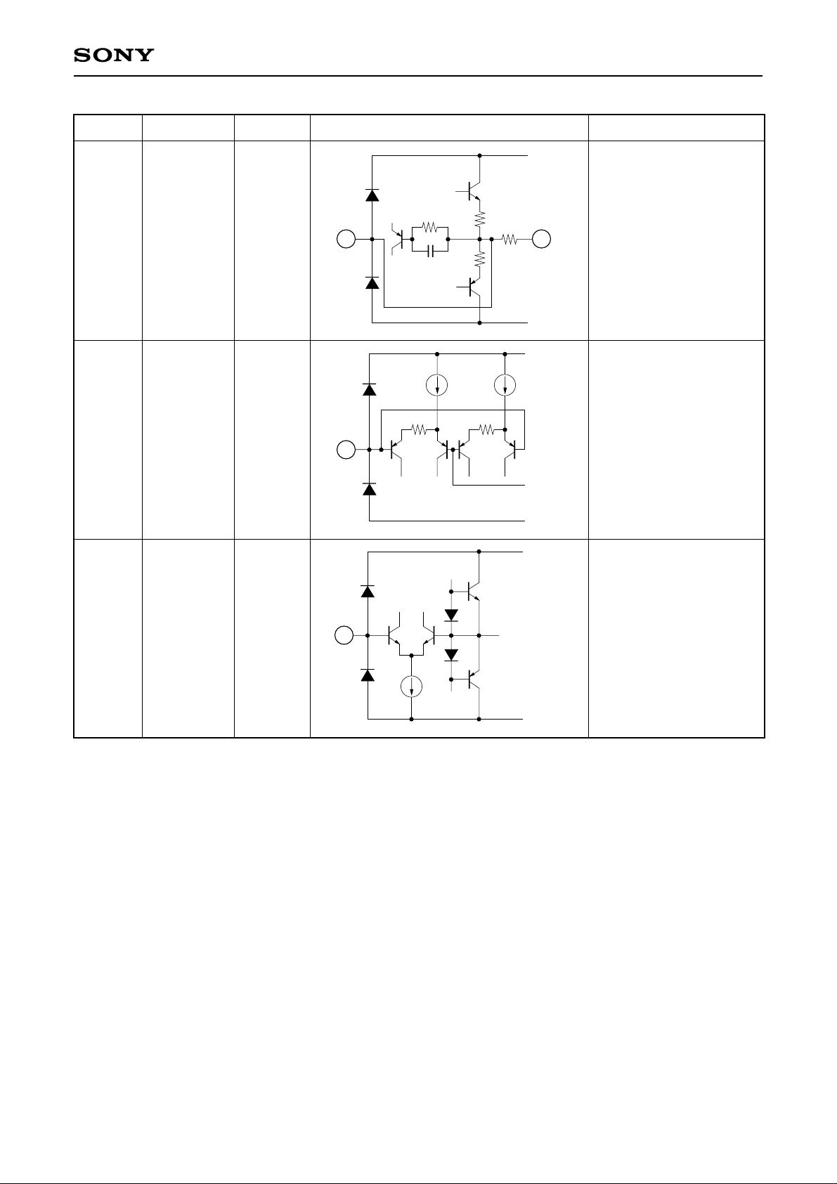
Pin Description (DCV values are for Vcc = 6.0V and VEE = –6.0V.)
Pin No. Symbol DCV (V) Equivalent Circuit Description
VCC
1 HLSMP 0 HLS main path input
2 MCTC –3.9
3 ZHSH 0
1
VEE
VCC
1.5k
2
9.2k
2p
VEE
VCC
2.6k
3
Time constant for the
MC2
DC cut capacitance for
the HLS/HF/SB detector
4 ZL2 0
VEE
VCC
VCT
16k
4
HF/LF/FB pass band
rectifier input
GND
– 3 –
Page 4

CXA1917AM/AS
Pin No. Symbol DCV (V) Equivalent Circuit Description
VCC
5
10.2k
5 LFIN 0 HLS/LF/FB-stage input
GND
VCC
1.5k
6 TCL1 –4.6
7 TCL2 –4.6
6
68k
VEE
VCC
7
300k
Primary time constant for
the HLS/LF/FB detector
Secondary time constant
for the HLS/LF/FB
detector
124k
VEE
VCC
500
8 SCINH 0 HLS/HF side chain input
8
500
VEE
– 4 –
Page 5
CXA1917AM/AS
Pin No. Symbol DCV (V) Equivalent Circuit Description
VCC
9 FBOH 0 HLS/HF/FB VCR output
1.6k
9
22
5.1k
VCT
22 FBOL 0 LLS/HF/FB VCR output
GND
VCC
10 TCF1H 0
11 TCF2H –4.6
18 TCF2L –4.6
12 TCS2H –4.6
10
11
18
12
20
80k
364k
340k
22k
2k
Primary time constant for
the HLS/HF/FB detector
VEE
VCC
Secondary time constant
for the HLS/HF/FB
detector
Secondary time constant
for the LLS/HF/FB
detector
VEE
VCC
Secondary time constant
for the HLS/HF/SB
detector
20 TCS2L –4.6
46k
– 5 –
4k
Secondary time constant
for the LLS/FB/SB
detector
VEE
Page 6
CXA1917AM/AS
Pin No. Symbol DCV (V) Equivalent Circuit Description
VCC
13 TCS1H –4.6
14 VCT 0
15 VEE –6.0
13
14
2k
80k
26k
500
500
Primary time constant for
the HLS/HF/SB detector
VEE
VCC
For dual power supply:
Ground
For single power supply:
VCT
GND
For dual power supply:
Negative power supply
For single power supply:
Ground
16 VCC 6.0 Positive power supply
VCC
1.5k
17 IREF –4.8 Reference current input
19 TCF1L –4.6
17
19
80k
VEE
VCC
1.5k
Primary time constant for
the LLS/HF/FB detector
VEE
– 6 –
Page 7
CXA1917AM/AS
Pin No. Symbol DCV (V) Equivalent Circuit Description
VCC
21 TCS1L –4.6
23 SCBOL 0
24
21
86k
70k
500
500
VEE
1.64MEG
500p
23
Primary time constant for
the LLS/HF/SB detector
VCC
LLS/HF side chain buffer
amplifier output
24 SCINL 0 LLS/HF side chain input
VEE
VCC
25 RECOUT 0
25
2k
17.5k
20p
200
500
20k 20k
200
500
47p
Recording (encoding)
output
28
28 MCBO 0 MC buffer feedback
26 ZHSL
VEE
VCC
3.6k
26
0
VEE
DC cut capacitance for
the LLS/HF/SB detector
– 7 –
Page 8
CXA1917AM/AS
Pin No. Symbol DCV (V) Equivalent Circuit Description
VCC
20k
500
27 HLSOUT 0 HLS output
27
47p
500
11k
26
VEE
VCC
22k
29 MC3IN 0 MC3 input
30 MC4IN 0 MC4 input
29
30
22k
VEE
VCC
VEE
– 8 –
Page 9
CXA1917AM/AS
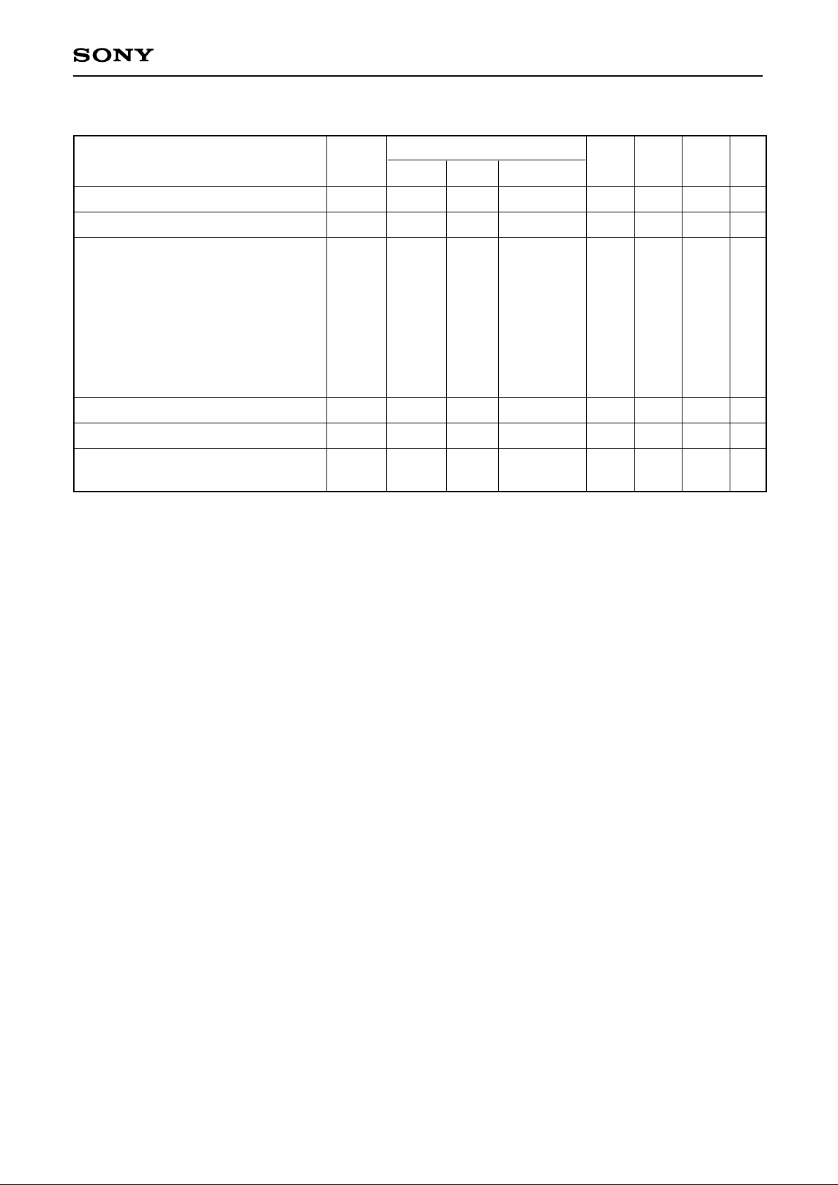
Electrical Characteristics
Characteristics Symbol
Operating voltage
Current consumption
Encoding characteristics (boost)
(1)
(2)
(3)
(4)
(5)
(6)
(7)
(8)
Signal handling
Total harmonic distortion
S/N ratio
(Ta = 25°C, Dolby level: –6dBm (= 388mVrms) at encoder input, Vcc = +6V, VEE = –6V)
Measurement conditions
VOPR
ICC
EB-1
EB-2
EB-3
EB-4
EB-5
EB-6
EB-7
EB-8
Vomax
THD
SNR
f (kHz)
1
2
0.05
0.3
12
0.3
2
0.05
12
1
1
Input
15dB
–60
–40
–40
–40
–20
–20
0
0
0
Other
THD ≤ 1%
No signal
THD = 1%
Rg = 600Ω
CCIR/ARM
Min.
±4.5
10.0
22.0
5.9
15.0
12.8
6.7
4.4
–2.9
–7.3
14.0
—
62.0
Typ.
15.0
23.5
7.4
16.5
14.3
8.2
5.9
–1.4
–5.8
16.0
0.01
65.0
Max. Unit
±6.5
20.0
25.0
8.9
18.0
15.8
9.7
7.4
0.1
–4.3
—
0.15
—
V
mA
dB
dB
dB
dB
dB
dB
dB
dB
dB
%
dB
– 9 –
Page 10
CXA1917AM/AS
Anaryzer
Distortion
Noise
Meter
CCIR/ARM
10k
R27
39n
C25
C30
R30
2.2n
8.2k
VCC (+6V)
R28
C45
C44
C42
C40
C34
R34
R31
C38
1
A
24k
0.47µ
0.1µ
0.22µ
47n
8.2n
1.5k
13k
C29 470p
1µ
C14 100n
16
17
18
19
20
21
22
23
24
25
26
27
28
CC
V
IREF
GND
TCF2L
TCF1L
TCS2L
TCS1L
FBOL
SCBOL
SCINL
ZHSL
HLSOUT
MCBO
2
RECOUT
V
EE
VCT
TCS1H
TCS2H
TCF2H
TCF1H
FBOH
SCINH
TCL2
TCL1
LFIN
ZL2
ZHSH
15
14
13
12
11
10
9
8
7
6
5
4
3
R23
33
C48
C46
C43
C41
C31
C26
C23
C7
EE (–6V)
V
0.1µ
0.22µ
0.47µ
0.1µ
8.2n
1µ
0.22µ
100n
3
C27
18k
680p
R26
10k
R24
39n
C24
22n
39k
C20
R19
39k
R16
C17
100n
10k
R12
C8
22n
R9
39k
Signal
Genarator
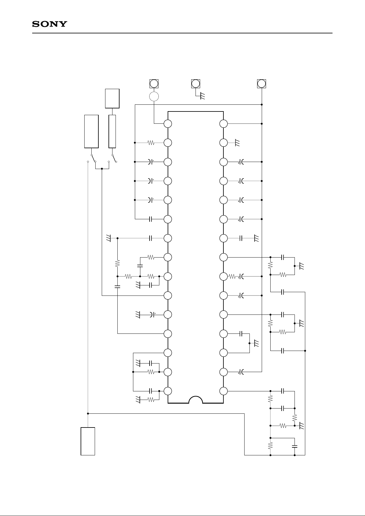
Electrical Characteristics Measurement Circuit
29
30
– 10 –
MC3IN
MC4IN
MCTC
2
HLSMP
1
C16
0.22µ
R20
R14
R10
5.1k
16k
27k
C21
C19
R15
C11
1.8n
1.8n
2.4k
100n
Page 11
CXA1917AM/AS
6
LINEOUT
C4
(–6dBm)
RECOUT
4.7µ
R27
C25
10k
39n
5
(–6dBm)
C9
4.7µ
C30
2.2n
R30
8.2k
C45
C42
CC (+6V)
V
R28
0.47µ
C44
0.22µ
C40
C34
R34
R31
C38
1
24k
33
R47
0.1µ
47
R45
47n
8.2n
1.5k
13k
C29 470p
1µ
C14 100n
16
17
18
19
20
21
22
23
24
25
26
27
28
CC
V
IREF
GND
TCF2L
TCF1L
TCS2L
TCS1L
FBOL
SCBOL
SCINL
ZHSL
HLSOUT
MCBO
2
RECOUT
V
EE
VCT
TCS1H
TCS2H
TCF2H
TCF1H
FBOH
SCINH
TCL2
TCL1
LFIN
ZL2
ZHSH
15
14
13
12
11
10
9
8
7
6
5
4
3
R48
R46
R25
33
47
33
C48
C31
C26
C23
C7
EE (–6V)
V
0.1µ
C46
C43
C41
8.2n
1µ
0.22µ
100n
3
0.22µ
0.47µ
0.1µ
R26
R19
18k
39k
C27
R24
C24
C20
R16
C17
680p
10k
39n
22n
39k
100n
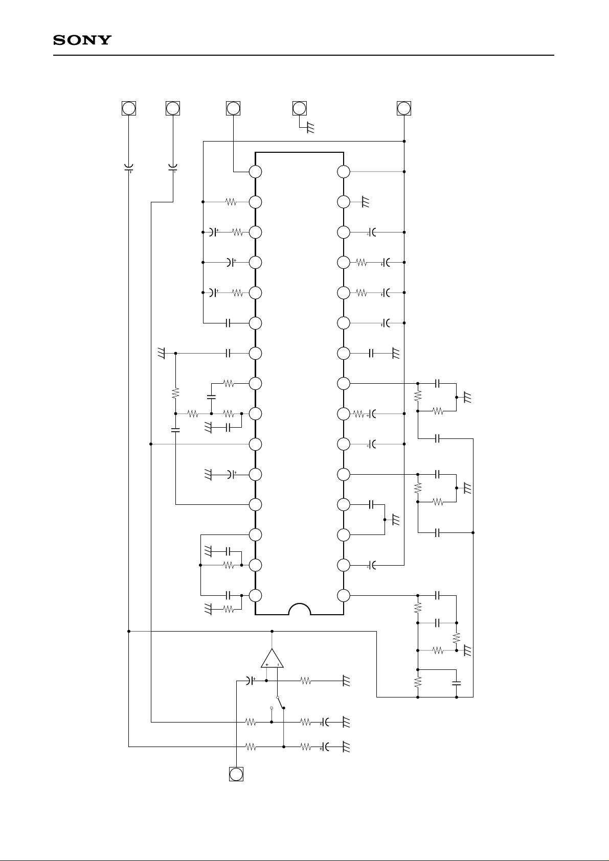
Application circuits shown are typical examples illustrating the operation of the devices. Sony cannot assume responsibility for
any problems arising out of the use of these circuits or for any infringement of third party patent and other right due to same.
Application Circuit
R12
10k
C8
22n
R9
39k
7
INPUT
29
30
C1
4.7µ
R4
12k
DECODE
R5
12k
(–25dBm)
MC3IN
MC4IN
R1
R3
ENCODE
R2
– 11 –
22k
1.5k
1.5k
C3
C2
33µ
33µ
MCTC
2
HLSMP
1
C16
0.22µ
R20
R14
R10
5.1k
16k
27k
C21
C19
R15
C11
1.8n
1.8n
2.4k
100n
Page 12

CXA1917AM/AS
Notes on Application
The CXA1917A is an encoding IC for the Dolby S type (NR). An external operational amplifier is required to
configure the decoder circuit. The Dolby level voltage of this IC is designed to be –6dBm (388mVrms), which is
the same as that of the CXA1562 and CXA1563 Dolby B-C type ICs. Therefore, it is possible to use the
CXA1562 or the CXA1563 to configure a B-C-S type switchable processor. The B-C-S type switchable
processor can be configured without requiring an external operational amplifier because the CXA1563 has a
built-in S-type changeover switch.
Power Supply
The CXA1917A will operate with either dual or single power supply. Connect VCT pin to GND pin when dual
power supply is used. Connect VEE pin to GND pin and open VCT pin when a single power supply is used. The
power supply half the Vcc generated inside the IC is generated at VCT pin.
The supply voltage range is from ±4.5V to ±6.5V and from 9V to 13V for dual and single power supplies,
respectively. Note, however, that the minimum supply voltage is determined by the maximum voltage
amplitude of external operational amplifier. Because general-purpose operational amplifiers have the
maximum voltage amplitude of approximately (Vcc – VEE) –2V, actual minimum supply voltages, which satisfy
the 15dB overload margin, are ±5.0V and 10V for dual and single power supplies, respectively. The supply
current does not depend so much on the supply voltage, but does depend on the signal level and frequency.
The maximum supply current in the worst case is approximately 25mA.
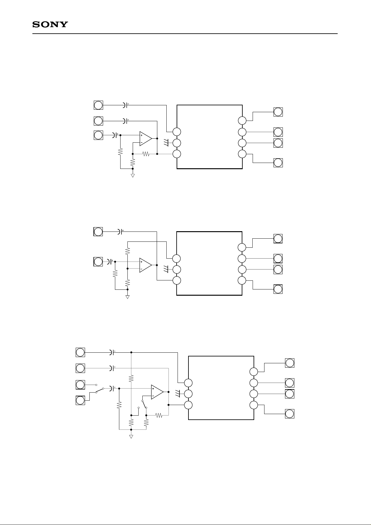
Recording Processor
Fig. 1 shows the recording processor. The gain is defined as follows:
GREC20 · Log (1 + R62/R63) ...... (1)
The processor in Fig. 1 has a gain of 14dB, therefore, input sensitivity is –20dBm (77.5mVrms). An input
sensitivity higher than –25dBm (44mVrms) is generally unacceptable due to noise performance, although this
is affected by the operational amplifier in the input circuit. An important characteristic for the external
operational amplifier is the noise performance for approximately an input impedance of 20kΩ. A bipolar input
type will be better than the JFET input type for the recording processor.
Playback Processor
Fig. 2 shows the playback processor. The gain is defined as follows:
GPB20 · Log (1 + R64/R65) ...... (2)
The processor in Fig. 2 has a gain of 20dB, therefore, the input sensitivity is –26dBm (39mVrms). Important
characteristics of the playback processor are the frequency response and the feedback loop stability, which
depend on the gain of the feedback loop gain and the slew rate of the external operational amplifier. The slew
rate has to be higher than 3V/µs. The loop gain can be estimated using the gain bandwidth product BG (Hz) of
the operational amplifier and the decode gain APB. The lower limit of BG/APB is approximately 500kHz, and
the recommended range is from 1 to 3MHz.
Switchable Processor
Fig. 3 shows the switchable processor. The gains are the same as in equations (1) and (2). An operational
amplifier is required with low noise, average slew rate (> 3V/µs), and wide bandwidth (≈ 10MHz) for this gain
setting. A bipolar input type operational amplifier with a wide bandwidth like those of the 4560 and the 4570 is
required of the switchable processor.
The processor in Fig. 3 may generate a significant switching noise, especially when S2 switch is make-breakmake type. When S2 switch is a make-to-make type or has a quick switching feature, the switching noise will
be within the range acceptable for cassette decks with output muting circuits.
– 12 –
Page 13
CXA1917AM/AS
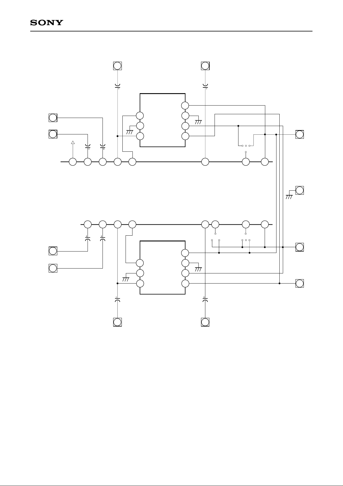
B-C-S Type Switchable Stereo Processor
Fig. 4 shows the stereo processor switchable to any B-C-S type mode. The operational amplifier is unnecessary,
because the CXA1563 is used for a B-C type processor and S-type changeover switch is built in the IC. It is
recommended that the S type mode be used for recording level calibration.
C61
C63
2.2µ
R61
56k
4.7µ
C62
4.7µ
R63
3k
VCT
A1
R62
12k
GND
RECOUT
5
GND
6
INPUT
7
Encoder Unit
VCC
GND
VEE
VCT
V
CC
1
1
2
3
4
GND
2
V
EE
3
VCT
4
RECOUT
(–6dBm)
LINEOUT
(–6dBm)
RECIN
(–20dBm)
5
6
7
Fig. 1. Recording Processor
RECOUT
(–6dBm)
LINEOUT
(–6dBm)
PBIN
(–26dBm)
RECIN
(–20dBm)
LINEOUT
(–6dBm)
PBIN
(–26dBm)
5
6
8
7
C62
4.7µ
6
VCC
1
1
VCC
GND
VEE
VCT
2
3
4
GND
2
V
EE
3
VCT
4
VCT
R64
18k
R65
2k
A1
GND
RECOUT
5
GND
6
INPUT
7
Encoder Unit
C64
2.2µ
8
R61
22k
Fig. 2. Playback Processor
C61
10µ
C62
S1
10µ
C63
2.2µ
R61
56k
R64
18k
R652kR63
3k
S2
A1
R62
12k
GND
RECOUT
5
GND
6
INPUT
7
Encoder Unit
VCC
GND
VEE
VCT
1
2
3
4
V
CC
1
2
GND
VEE
3
VCT
4
VCT
Fig. 3. Switchable Processor
– 13 –
Page 14
CXA1917AM/AS
PBIN1
LINEIN1
12
11
VCT
C11
1µ
VCT
2728
2
C12
1µ
PBIN1
PBIN2
LINE OUT1
C13
1µ
26
LINEIN1
LINEIN2
3
13
GND
22
LINEOUT1
LINEOUT2
7
21
8
5
6
7
SIN1
SIN2
Encoder
Unit 1
RECOUT
GND
INPUT
CXA1563
CC
V
GND
V
EE
VCT
1
2
3
4
REC OUT1
14
C16
1µ
GND
18
RECOUT1
RECOUT2
11
12
SSW
PB
MPX
OFF
16
13
MPX
ON
MODE
NRSW
15
14
CC
V
GND
GND
CC
V
1
GND
2
LINEIN2
PBIN2
22
21
C21
1µ
C22
1µ
Encoder
S
GND
C23
1µ
23
LINEOUT2
RECOUT
5
GND
6
INPUT
7
Unit 2
VCC
GND
V
VCT
EE
1
2
3
4
GND
C26
1µ
24
RECOUT2
Fig. 4. B-C-S Switchable Stereo Processor
B/C
OFF
C
B
VEE
3
VCT
4
– 14 –
Page 15
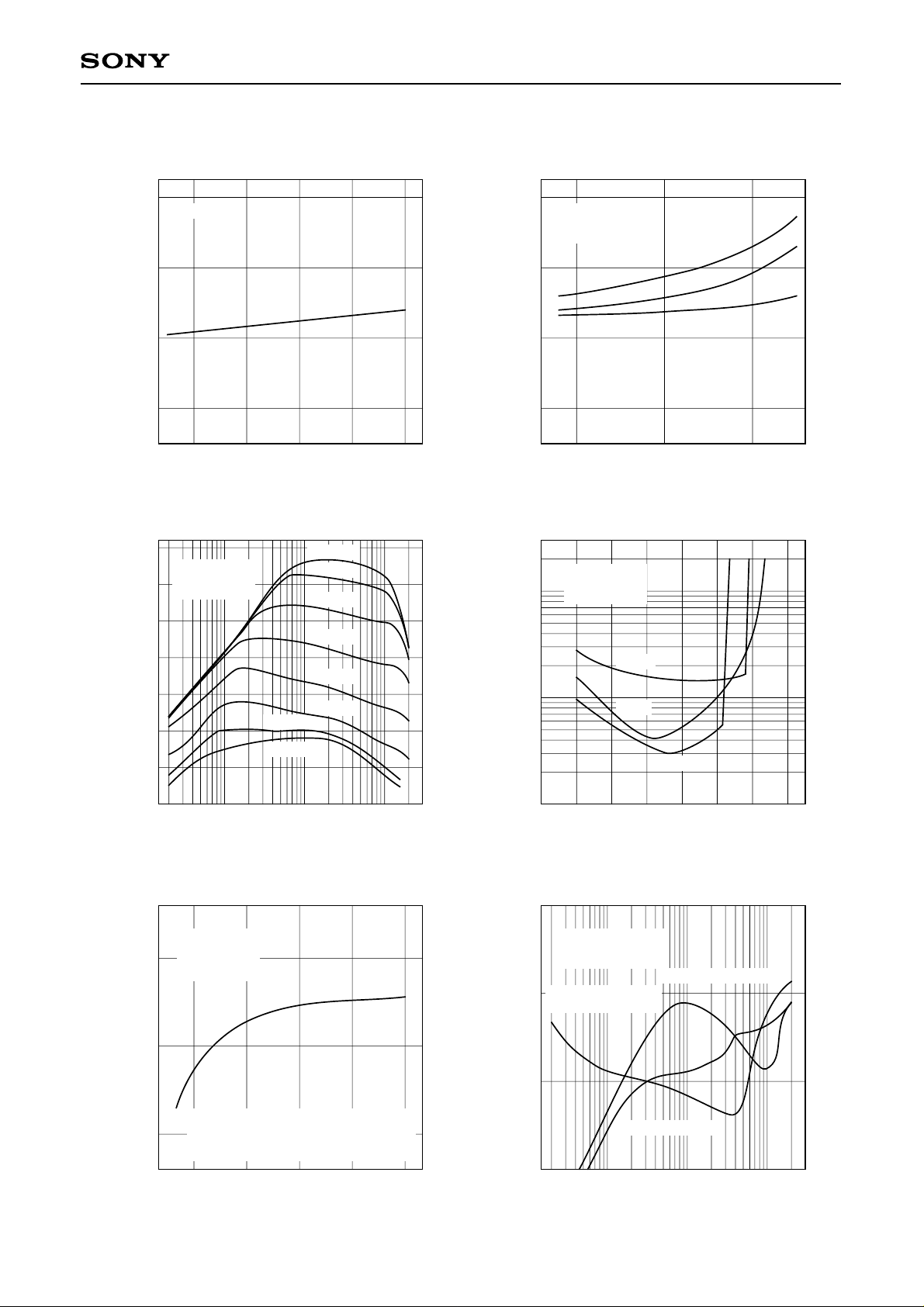
Example of Representative Characteristics
CXA1917AM/AS
Current consumption vs. Supply voltage
18
No signal
16
14
– Current consumption [mA]
CC
I
12
8 10121416
VCC – VEE – Supply voltage [mA]
Encoding characteristics
25
VCC = +6V
VEE = –6V
20
0dB = –6dBm
15
10
5
Encoding boost [dB]
0
–5
–60dB
–50dB
–40dB
–30dB
–20dB
–10dB
0dB
+10dB
Current consumption vs. Input level
18
VCC = +6V
VEE = –6V
0dB = –6dBm
16
14
– Current consumption [mA]
CC
I
12
–10 0 10
Encoding input level [dB]
10kHz
1kHz
100Hz
Total harmonic distortion characteristics
VCC = +6V
VEE = –6V
1.0
0dB = –6dBm
100Hz
0.1
Total harmonic distortion [%]
1kHz
10kHz
–10
Overload margin vs. Supply voltage
VCC = +6V
VEE = –6V
20
0dB = –6dBm
f = 1kHz
15
Overload margin [dB]
Overload margin:
Encoding input level when 1% of
10
total harmonic distortion is generated
at the encoding output
8 10121416
VCC – VEE – Supply voltage [V]
Frequency [Hz]
30k
10k3k1k30010030
0.01
–10
–5 0 5 10 15
Output level [dB]
20
Ripple rejection
–10
VCC – VEE = 12V
Vripple = –20dBm
Encode Mode
VCC (Single Supply)
–20
–30
Ripple rejection [dB]
–40
C = 47µ (14pin)
VCC (Dual Supply)
VEE (Dual Supply)
Frequency [Hz]
10k3k1k30010030
30k
– 15 –
Page 16
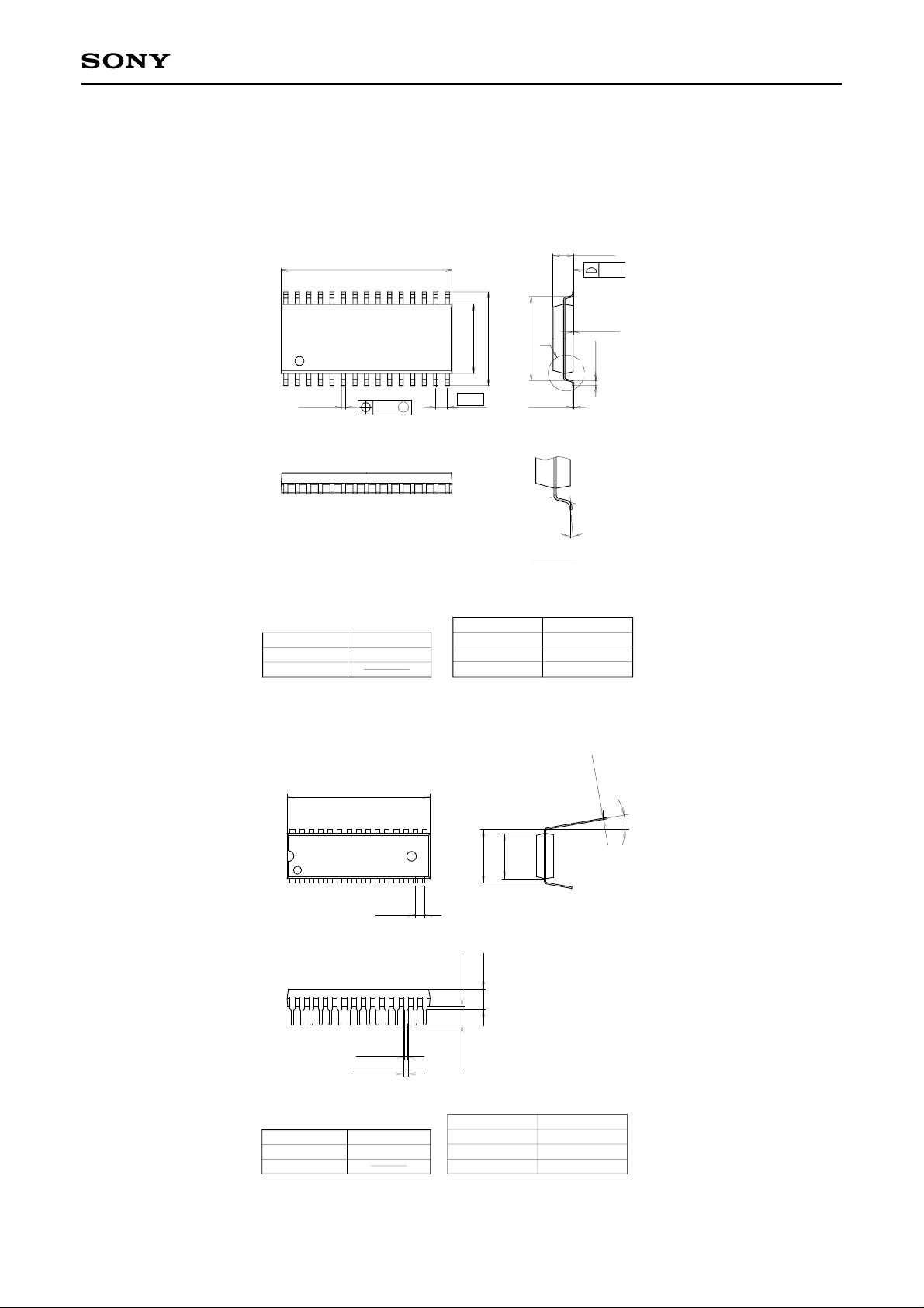
Package Outline Unit: mm
CXA1917AM
30
1
0.45 ± 0.1
30PIN SOP(PLASTIC)
+ 0.4
18.8 – 0.1
0.2
M
CXA1917AM/AS
+ 0.4
2.3 – 0.15
0.1
16
+ 0.2
+ 0.3
7.6 – 0.1
15
1.27
10.3 ± 0.4
(9.3)
0.2 – 0.05
0.1 – 0.05
A
0.5 ± 0.2
+ 0.1
CXA1917AS
SONY CODE
EIAJ CODE
JEDEC CODE
30
1
SOP-30P-L03
SOP030-P-0375
30PIN SDIP (PLASTIC)
+ 0.4
26.9 – 0.1
1.778
PACKAGE STRUCTURE
PACKAGE MATERIAL
LEAD TREATMENT
LEAD MATERIAL
PACKAGE WEIGHT
16
15
0.5 MIN
10.16
+ 0.4
3.7 – 0.1
+ 0.3
8.5 – 0.1
0° to 10°
DETAIL A
EPOXY RESIN
SOLDER PLATING
42/COPPER ALLOY
0.7g
+ 0.1
0.25 – 0.05
0° to 15°
SONY CODE
EIAJ CODE
JEDEC CODE
0.5 ± 0.1
0.9 ± 0.15
SDIP-30P-01
SDIP030-P-0400
3.0 MIN
PACKAGE STRUCTURE
MOLDING COMPOUND
LEAD TREATMENT
LEAD MATERIAL
PACKAGE WEIGHT
– 16 –
EPOXY / PHENOL RESIN
SOLDER/PALLADIUM
COPPER ALLOY
1.8g
PLATING
 Loading...