

Page 1

—1—
E95432-TE
Sony reserves the right to change products and specifications without prior notice. This information does not convey any license by
any implication or otherwise under any patents or other right. Application circuits shown, if any, are typical examples illustrating the
operation of the devices. Sony cannot assume responsibility for any problems arising out of the use of these circuits.
Absolute Maximum Ratings (Ta=25 °C)
• Supply voltage VCC 12 V
• Operating temperature Topr –20 to +75 °C
• Storage temperature Tstg –65 to +150 °C
• Allowable power dissipation PD 1.8 W
Operating Conditions
Supply voltage VCC 9±0.5 V
Description
The CXA1871S is a bipolar IC which integrates the
NTSC and PAL color TV luminance signal
processing, chroma signal processing, sync signal
processing, and RGB signal processing onto a
single chip.
Features
• I2C bus compatible. Various types of adjustments
and user controls performed with two bus lines
SCL and SDA.
• H and V oscillation frequencies made non-
adjusting with a countdown system.
• Non-adjusting Y system filters (chroma trap, delay
line)
• Built-in V picture distortion correction circuit
• Built-in delay line aperture compensation
• Auto cut-off function for automatic CRT cut-off
adjustment and compensation for changes with
time
• Multiple inputs
Composite Video 2 systems
(Built-in 2-input, 1-output video switch)
Y/C separation input: 1 system
On screen display input: 1 system
• Multiple system configuration possible using a non-
adjusting SECAM chroma decoder.
Applications
Color TV
Structure
Bipolar silicon monolithic IC
NTSC/PAL Y/C/Jungle
48 pin SDIP (Plastic)
CXA1871S
Page 2

—2—
CXA1871S
G CUTOFF
DYNAMIC
COLOR
TRAP
DELAY
SHARPNESS
CLAMP
AUTO
PEDESTAL
Y/C MIX
CLAMP
DELAY
TOT
ACC
B.G.
ACC
DET.
COLOR
KILLER
PHASE
DET.
LPF
PHASE
SHIFT
CHROMA
DET.
Y IN
V1 IN
V2 IN
C IN
V
CC
APC
X PAL2
A PED
B-Y OUT
I
2
C BUS
DECORDER
SCL
SDA
IREF
H SYNC
REG
REGU
LATOR
H.SYNC
SEP
AFC
CERA
32f
H
VCO
1/32
2f
H
PHASE
DET
XRAY
PHASE
SHIFT
H.DRIVE
XRAY
HD
SCP
V SYNC
V.SYNC
SEP
V PLS
VOSC
V COUNT
DOWN
VOSC
V COMPENSATION
V ZOOMING
VD
ABL IN
ABL
H PHASE
AKB
TIMING
IK
CLAMP
BOUT
GOUT
ROUT
ABL LPF
V LPF
V HOLD
HP
IREF
PHASE
DET.
SW OUT
0/6DB AMP
IN SW
SW GAIN
TRAP SW
TOT SW
SUB HUE
OSD
DRIVE
G DRIVE
B DRIVE
AKB
R S/H
G S/H
B S/H
IK
B CUTOFF
DC TRAN
SHARPNESS
AFC HLOCK
NR
REF
GAMMA
GAMMA
OSD
MIX
VEX
C MODE
HV COMP
V SHIFT
V SIZE
V LIN
S CORR
V OFF
ABL
PMUTE
R OFF
G OFF
B OFF
BLK
SUB CONT
PICTURE
PICTURE
DC
SHIFT
SUB
CONT
BRIGHT
BRIGHT
SUB BRIGHT
DY COL
NR
HUE
SUB COLOR
PRE OVER
YM
RGB SW
BLUE
BLACK
OSD
BLK
OSD BLK
XRAY
41
40
38 43
39
37 36 34 33 32
42
44
8
31
29
30
27
28 26
19
21
23
18 20 222414
OSD R
OSD G
OSD B
15 16 17
5
11
6
7
10
12
25
9
AXIS
J GND
35
50/60
HUE
4.43/3.58
SW
2
CHROMA
VCO
SECAM
SECAM
REF
1
V GND
13
X' TAL PIN
DEM
AXIS
X PAL1
3
X NTSC
4
47 48
R-Y OUT
AXIS
NT/PAL
ID AXIS
PAL ID
F.F
2f
H
NT/PAL
B-Y IN
45
R-Y IN
46
COLOR
DET SW
CLAMP
COLOR
EXT
COLOR
NT/PAL
KILLER
Block Diagram
Page 3

—3—
CXA1871S
Pin Configuration
R-Y IN
R-Y OUT
B-Y OUT
B-Y IN
V2 IN
SDA
SCL
V SYNC
H SYNC
SCP
REG
IREF
AFC
CERA
J GND
HP
XRAY
HD
V PLS
V LPF
V OSC
ABL LPF
VD
ABL IN
X NTSC
X PAL2
X PAL1
SECAM REF
V
CC
APC
V1 IN
A PED
Y IN
C IN
V GND
OSD BLK
OSD R
OSD G
OSD B
R S/H
R OUT
G S/H
G OUT
B S/H
B OUT
IK
V HOLD
SW OUT
1
2
3
4
5
6
7
8
9
10
11
12
13
14
15
16
17
18
19
20
21
22
23
24 25
26
27
28
29
30
31
32
33
34
35
36
37
38
39
40
41
42
43
44
45
46
47
48
Page 4

—4—
CXA1871S
Pin Description
Pin
Symbol
Pin
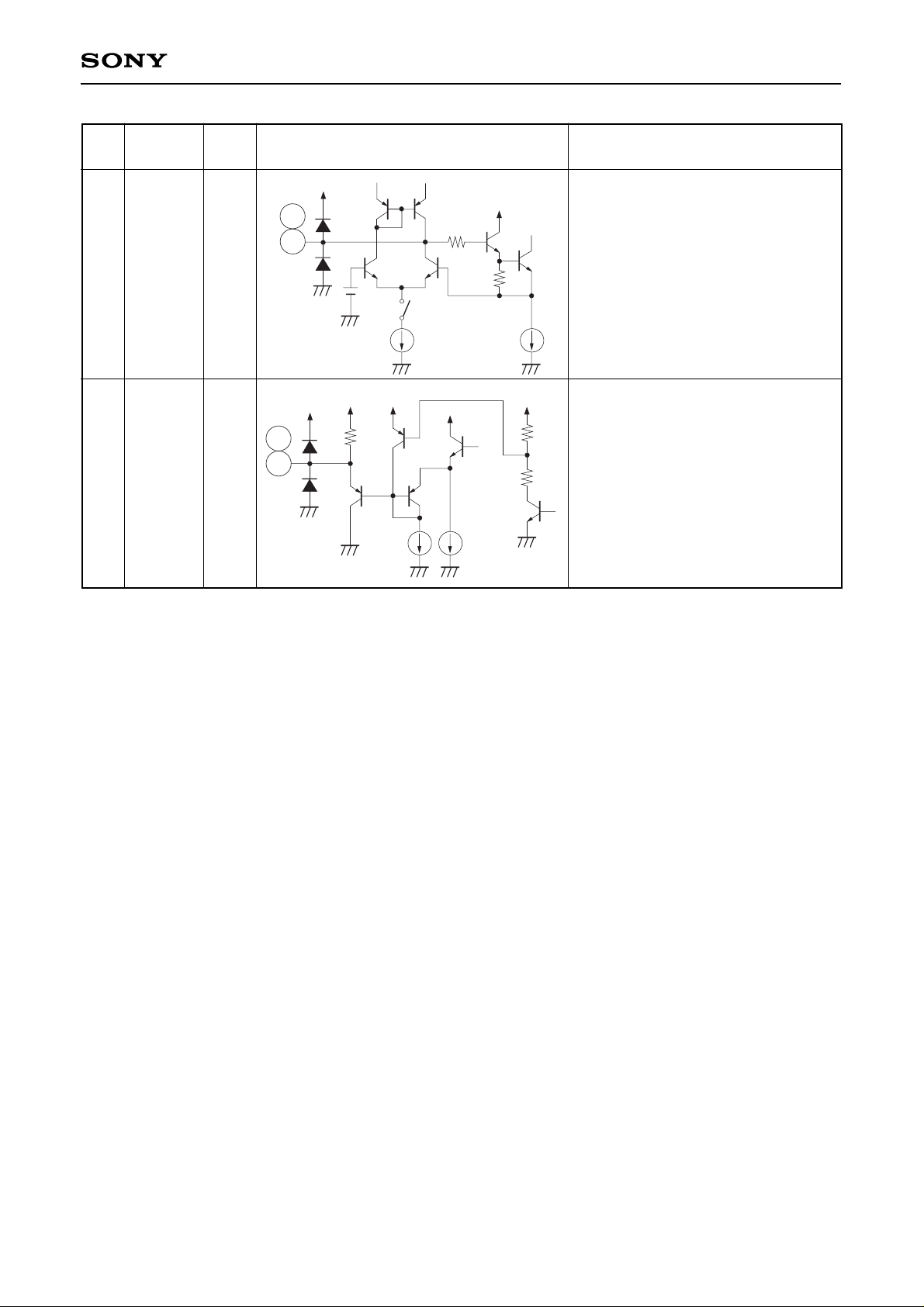
Equivalent circuit Description
No. voltage
VCC
6 k
20 k
20 p
V
CC VCC
1
1
2
3
4
5
6
7
25
SECAM
REF
X PAL 1
X PAL 2
X NTSC
APC
V
CC
V1 IN
V2 IN
1.3 V
2.6 V
5 V
9 V
2 V
When the IC is in the SECAM
identification mode, the 4.43 MHz
VCO oscillation waveform is output
from this pin only during the VBLK
period centering on DC = 1 V. If
current of 150 µA is led from this pin
during this identification mode, the IC
switches to the SECAM mode. In the
SECAM mode, DC = 5 V.
Crystal oscillator connection pins.
Connect the PAL/N and 4.43 MHz
crystals to Pin 2, the PAL/M crystal to
Pin 3, and the NTSC crystal to Pin 4.
APC lag-lead filter CR connection pin.
Power supply pin.
Video switch input pins. Sync tip
clamping is performed, so input via
capacitors.
1.2 k
25 k
1.2 k
5
VCC
VCC
150
7
VCC
25
4 k
500
2
3
4
VCC
VCC
Page 5

—5—
CXA1871S
Pin
Symbol
Pin
Equivalent circuit Description
No. voltage
2 k
30 k
12 k
25 k
500
9
VCC
VCC
VCC
8
9
10
11
V HOLD
SW OUT
Y IN
A PED
0.7 V
—
3.5 V
3.5 V
Peak hold pin for V sync separation.
Connect a capacitor.
Video switch output pin.
Y signal input pin. Input via a
capacitor.
Standard input level: 2 Vp-p
Auto pedestal (black stretch) black
peak hold pin. Connect a capacitor.
50 k
1.2 k
10
V
CC
VCC
16 k
20 k
20 k
1.2 k
11
VCC
VCC VCC VCC
55 k
VCC
8
150
1 k
50 k
Page 6

—6—
CXA1871S
Pin
Symbol
Pin
Equivalent circuit Description
No. voltage
6 k 6 k
30 k
30 k
12
V
CC
12
13
14
15
16
17
18
20
22
C IN
V GND
OSD BLK
OSD R
OSD G
OSD B
R S/H
G S/H
B S/H
—
—
—
—
—
Chroma signal input pin.
Standard input level (burst level)
: 570 mVp-p
Video system (Y/C/RGB) GND pin.
Blanking signal input pin for OSD
RGB input.
0 to 1 V: Blanking not performed.
2 to 3 V: Signal from Y IN/C IN
lowered by –6 dB.
4 to 6 V: R, G and B outputs become
lower than black level.
Digital R, G and B signal input pins for
on screen display.
0 to 1 V: No OSD display.
2 to 3 V: OSD level 49 IRE (34 IRE)
4 to 6 V: OSD level 96 IRE (67 IRE)
Figures in parentheses are for when
the I2C OSD register is set to 0.
Sample-and-hold pins for R, G and B
AKB (Auto Kinetic Bias). Connect to
GND via capacitors.
40 k
15 k
2 k
60 k
30 k
2 k
60 k
30 k
2 k
60 k
14
30 k
2 k
VCC VCC
VCC
15
16
17
VCC
1.2 k
18
20
22
VCC
Page 7

—7—
CXA1871S
Pin
Symbol
Pin
Equivalent circuit Description
No. voltage
19
21
23
24
26
27
28
R OUT
G OUT
B OUT
IK
ABL IN
VD
ABL LPF
—
—
—
—
—
R, G and B output pins.
Inputs the signal obtained by
converting the CRT beam current (IK)
into voltage. Connect to an emitter
follower via a capacitor.
ABL voltage input pin.
Vertical deflection sawtooth wave
output pin.
ABL signal LPF pin. Connect a
capacitor. If the AKB loop is unstable
when the power is turned on, this pin
is lowered to around 0.3 V.
150
5 k
19
21
23
VCC
VCC VCC
150
24
V
CC
VCC
150
10 k
30 k
26
V
CC
5 k
3 k
3 k
15 k
24 k
27
VCC
VCC
VCC
VCC
24 k
100 k
35 k
10 k
28
VCC VCC
VCC
Page 8

—8—
CXA1871S
Pin
Symbol
Pin
Equivalent circuit Description
No. voltage
29
30
31
32
33
V OSC
V LPF
V PLS
HD
XRAY
—
5 V
—
—
—
Connect a capacitor to generate the V
sawtooth wave.
Connect a capacitor to hold the AGC
voltage which maintains the V
sawtooth wave at a constant
amplitude.
V pulse output pin. A negative
polarity pulse 3 to 3.5 H width is
output from this pin.
High level: 4.5 V
Low level: 0 V
H drive output pin. This pin is output
at the open collector.
X-ray protection circuit input pin.
When a pulse with a width of 7 V or
more is input, HD output becomes low
and R, G and B outputs are blanked.
This status is maintained until the
power supply is turned off.
Vilmax = 2.4 V
Vihmin = 3.0 V
100
100
29
VCC
VCC
VCC
VCC
20 k
20 k
32
19 k
30 k
40 k
30 k
63 k
27 k
33
VCC
VCC VCC
VCC
VCC
30
VCC
74 k
18 k
31
VCC
VCC
Page 9

—9—
CXA1871S
Pin
Symbol
Pin
Equivalent circuit Description
No. voltage
34
35
36
37
38
HP
J GND
CERA
AFC
IREF
3.3 V
(at no
signal)
—
2.3 V
3.2 V
2.6 V
H pulse input pin. Inputs a 3 to 5 Vp-p
signal via a capacitor.
Jungle system (H/V) GND pin.
Connect a 32 fh (503.5 kHz) ceramic
oscillator.
AFC lag-lead filter CR connection pin.
Connect a 15 kΩ resistor between this
pin and GND.
VCC
10 k
28 k
V
CC
VCC
330
36
VCC
46 k
1.2 k
V
CC
VCC
37
150
20 k
38
VCC
VCC
10 k
60 k
VCC
VCC
34
Page 10

—10—
CXA1871S
Pin
Symbol
Pin
Equivalent circuit Description
No. voltage
39
40
41
42
43
44
REG
SCL
SDA
SCP
H SYNC
V SYNC
7 V
—
—
2.6 V
3.8 V
Regulator pin for voltage generated
internally from VCC. Connect a
capacitor for stabilization.
I2C bus SCL (Serial Clock) and SDA
(Serial Data) pins.
Vilmax = 1.5 V
Vihmin = 3 V
Volmax = 0.4 V
Outputs BGP, HBLK and VBLK as
SCP (Sand Cathle Pulse).
The Typ. waveform is as follows.
H sync separation input pin. Inputs a
2 Vp-p video signal via a capacitor
and resistor.
V sync separation input pin. Inputs a
2 Vp-p video signal via a capacitor
and resistor.
150
14 k
24 k
20 k
43
10 µA
V
CC
VCC
150
10 k
26 k
31 k
10 k
20 k
44
20 µA
1.2 k
40 k
4 p
39
50 µA
VCC
VCC VCC
VCC
VCC
4 k
4 k
VCC
40
41
VCC
1.2 k
VCC
500 µA
VCC
VCC
BGP
H,VBLK
0.3 V
2.5 V
5.0 V
Page 11
—11—
CXA1871S
Pin
Symbol
Pin
Equivalent circuit Description
No. voltage
1.2 k
100 µA
VCC
45
46
BGP
VCC
50 k
45
46
47
48
R-Y IN
B-Y IN
B-Y OUT
R-Y OUT
5.2 V
5 V
Color difference signal input pins.
Input via capacitors.
Standard input level
B-Y: 1.33 Vp-p
R-Y: 1.05 Vp-p
Color difference signal output pins.
Standard input level
B-Y: 0.665 Vp-p
R-Y: 0.525 Vp-p
20 k
80 k
10 k
47
48
VCC
VCC VCC VCC
Page 12

—12—
CXA1871S
Video In: Sig-H2,H3
AFC: 0
Video In: Sig-H6
AFC: 0
Video In: Sig-H7
AFC: 0
Video In: Sig-H6
AFC: 1
Video In: Sig-H7
AFC: 1
Video In: Sig-H6
AFC: 2
Video In: Sig-H7
AFC: 2
Video In: Sig-H1
Video In: Sig-H1
Video In: Sig-H1
Video In: Sig-Y1
HPHASE: F
Video In: Sig-Y1
HPHASE: 7
Video In: Sig-Y1
HPHASE: 0
Video In: Sig-Y1
2
3
4
5
6
7
8
9
10
11
12
13
14
15
16
17
18
Horizontal free running
frequency
Horizontal sync pull-in
range
AFC gain 1
AFC gain 2
AFC gain 3
HD output pulse width
HD output high level
HD output low level
Horizontal phase
operating range 1
Horizontal phase
operating range 2
Horizontal phase
operating range 3
HP blanking delay
time 1
HP blanking delay
time 2
SCP BGP output level
SCP BLK output level
SCP low level
Overvoltage protection
circuit VTH
H system items
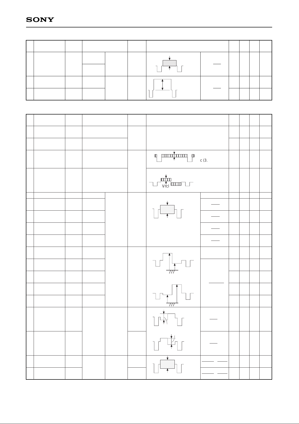
Electrical Characteristics
Setting conditions
• Ta = 25 °C, VCC = 9 V
• I2C bus register should be set to “I2C Bus Register Initial Settings”.
No.
Item Symbol
Measurement
Measurement
Measurement method
conditions pin
Min. Typ. Max. Unit
70 105 140 mA
1
Current consumption 1 ICC1 6 Measure the VCC pin inflow current.
No. Item Symbol
Measurement
Measurement
Measurement method
conditions pin
Min. Typ. Max. Unit
15.47 15.65 15.83 kHz
–400 — 400 Hz
0.12 0.30 0.48 µs
— 0.5 — µs
0.75 1.2 1.75 µs
24 26 28 µs
8.7 9 — V
0.5 0.8 1.1 V
–4.3 –3.3 –2.3 µs
–1.5 –0.5 0.5 µs
1.3 2.3 3.3 µs
— 100 — ns
— 100 — ns
4 5.0 6 V
2.5 V
0.3 V
2.4 2.6 2.8 V
Hfree
∆H
AFCmax
AFCcen
AFCmin
HD, W
HD, H
HD, L
HPHmax
HPHcen
HPHmin
HPBLK1
HPBLK2
VSB
VSBL
VSL
XVTH
Check that I
2
C register HLOCK is 1.
AFCmax=t1-t2
AFCcen=t1-t2
AFCmin=t1-t2
t1: Video In: Time from fall
of Sig-H6 to rise of Pin 34.
t2: Video In: Time from fall
of Sig-H7 to rise of Pin 34.
32
34
34
34
32
23
34
23
34
42
32
VSL
VSBL
VSB
Pin 23
Pin 34
HPBLK1
HPBLK2
Pin 23
HPH
HD,H
HD,L
HD,W
Check that HD appears at 2.4 V and disappears
at 2.8 V.
Page 13

—13—
CXA1871S
Video In:Sig-V1
V SHIFT:F
V SHIFT:0
V SHIFT:1F
V SIZE:0
V SIZE:3F
S CORR:0
S CORR:F
V LIN:0
V LIN:F
HV COMP: 0,
Pin 26: 6 V
HV COMP: 7,
Pin 26: 6 V
HV COMP: 0,
Pin 26: 0 V
HV COMP:7,
Pin 26: 0 V
19
20
21
22
23
24
25
26
27
28
29
30
31
V PLS high level
V PLS low level
VD output
center voltage
V SHIFT
variable range 1
V SHIFT
variable range 2
V SIZE
variable range 1
V SIZE
variable range 2
S CORR
variable range 1
S CORR
variable range 2
V LIN
variable range 1
V LIN
variable range 2
V zooming 1
V zooming 2
V system items
No. Item Symbol
Measurement
Measurement
Measurement method
conditions pin
Min. Typ. Max. Unit
4 4.5 5 V
0 0.1 0.5 V
2.75 2.9 3.05 V
–140 –125 –115 mV
110 120 140 mV
0.9 1.1 1.2 V
1.5 1.65 1.8 V
45 65 85 mV
–55 –35 –15 mV
90 120 140 mV
60 90 110 mV
0 3 15 mV
60 80 100 mV
VPLS, H
VPLS, L
VDcen
VSHIFT–
VSHIFT+
VSIZE–
VSIZE+
∆Sa
∆Sc
∆La
∆Lc
∆VZ1
∆VZ2
Vb
Vb-VDcen
Vb-VDcen
Vc-Va
Vc-Va
Vsa=Va
Vsc=Vc
Va-Vsa
Vc-Vsc
Vla=Va
Vlc=Vc
Va-Vla
Vc-Vlc
Vsmin=
Vc-Va
Vsmax=
Vc-Va
Vsmin(Vc-Va)
Vsmax(Vc-Va)
31
27
Video
In:
Sig-V1
Vc
Vb
Va
GND
Pin 27
VTRIG
0.1 ms
8.75
ms
16.57
ms
VPLS, L
VPLS, H
Page 14

—14—
CXA1871S
Video In:Sig-Y1
SUBCONT: F
SUBCONT: 0
TRAP SW: 0
TRAP SW: 1
TRAP SW: 0
TRAP SW: 1
SHARP
NESS: F
SHARP
NESS: 7
SHARP
NESS: 0
DELAY=0
DELAY=2
DC TRAN: 0
DC TRAN: 7
Pin 11: 3 V
Pin 11: 5 V
Pin 11: 3 V
Pin 11: OPEN
32
33
34
35
36
37
38
39
40
41
42
43
44
45
R output level
Sub-contrast
variable range 1
Sub-contrast
variable range 2
Trap attenuation 1
Trap attenuation 2
Sharpness
characteristics 1
Sharpness
characteristics 2
Sharpness
characteristics 3
RGB output
frequency response 1
RGB output
frequency response 2
DC transmission
rate 1
DC transmission
rate 2
Auto pedestal
operation 1
Auto pedestal
operation 2
Y system items
No. Item Symbol
Measurement
Measurement
Measurement method
conditions pin
Min. Typ. Max. Unit
— 2.5 — V
2.2 2.7 3.2 dB
–3.8 –3.3 –2.8 dB
— –30 –20 dB
— –30 –20 dB
5.5 7.0 8.5 dB
1.5 2.5 4.5 dB
–7.5 –5.5 –3.0 dB
–6 –3.0 0 dB
–7 –4.2 –1 dB
96 99 100 %
73 78 85 %
280 340 400 mV
80 130 170 mV
VR
Gsc, max
Gsc, min
ATT
trap1
ATT
trap2
Gsh, max
Gsh, cen
Gsh, min
Gfreq1
Gfreq2
Gdt1
Gdt2
Vdp1
Vdp2
20log
Vsc1
VR
20log
Vsc2
VR
20log
Vtr2
Vtr1
20log
Vtr2
Vtr1
20log
Vs2
Vs1
20log
Vf2
Vf1
20log
Vf2
Vf1
Vdw-Vdb
Vdpp
Vdw-Vdb
Vdpp
Voff-Von
Voff-Von
19
19
19
19
19
21
23
19
21
23
19
19
19
Video In:
Sig-Y1
Video In:
Sig-Y2
fsc=
3.58 MHz
Video In:
Sig-Y2
fsc=
4.43 MHz
Video In:
Sig-Y4
Video In:
Sig-Y5
Video In:
Sig-Y4, Y6
Video In:
Sig-Y4, Y6
Video In:
Sig-Y3
Video In:
Sig-Y1
Video In:
Sig-H1
Video In:
Sig-Y3
Video In:
Sig-Y1
Video In:
Sig-H1
Video In:
Sig-H1
Video In:
Sig-Y10
VR
Vsc1
Vsc2
Vtr1
Vtr2
Vs1
(Sig-Y4)
Vs2
(Sig-Y5)
Vf1
(Sig-Y4)
Vf2
(Sig-Y6)
Vdpp
Vdw
Vdb
Vdpp
Vdw
Vdb
Voff
Von
Voff
Von
Vtr1
Vtr2
Vf1
(Sig-Y4)
Vf2
(Sig-Y6)
Page 15
—15—
CXA1871S
NR: 1
NR: 0
SW GAIN: 1
SW GAIN: 0
46
47
48
NR operation
SW gain 1
SW gain 2
No. Item Symbol
Measurement
Measurement
Measurement method
conditions pin
Min. Typ. Max. Unit
–6 –4.5 –3 dB
5.5 6 6.5 dB
–0.5 0 0.5 dB
Gnr
Gsw1
Gsw2
20log
Von
Voff
20log
Vout
Vin
19
7, 25
9
Video In:
Sig-Y7
Video In:
Sig-Y1
Voff
Von
Vin
(Pins 7 and 25)
Vout (Pin 9)
Video-In: Sig-H1
C In: Sig-C1, C2
Video-In: Sig-H1
C In: Sig-C1, C2
Video-In: Sig-H1
COLOR: 3F
SUBCOLOR: F
Video-In: Sig-H1
C In: Sig-C3
COLOR: 3F
SUBCOLOR: F
COLOR: 3F
COLOR: 0
SUB COLOR
: F
SUB COLOR
: 0
HUE: 3F
HUE: 0
SUB HUE: F
SUB HUE:0
AXIS: 0
AXIS: 0
Check that the burst frequency is changed to
3579545 ±350 Hz and pulled in.
Check that the burst frequency is changed to
4433619 ±350 Hz and pulled in.
49
50
51
52
53
54
55
56
57
58
59
60
61
62
63
64
65
66
APC pull-in
range 1
APC pull-in
range 2
Carrier leak
Residual carrier
level
Color output level
Color variable
range 1
Color variable
range 2
Sub-color variable
range 1
Sub-color variable
range 2
Hue variable
range 1
Hue variable
range 2
Hue variable
range 3
Sub-hue variable
range 1
Sub-hue variable
range 2
Detective axis R1
Detective axis G1
Detective output
ratio R1
Detective output
ratio G1
C system items
No. Item Symbol
Measurement
Measurement
Measurement method
conditions pin
Min. Typ. Max. Unit
–350 — 350 Hz
–350 — 350 Hz
— — 50 mV
— — 200 mV
0.6 0.9 1.2 V
5.6 6.3 6.9 dB
— –50 –40 dB
2.1 2.7 3.3 dB
–5.4 –3.7 –2.0 dB
–10 0 10 deg
–54 –44 –34 deg
23 33 43 deg
–21 –15 –9 deg
8 13 20 deg
105 112 119 deg
244 251 259 deg
0.7 0.8 0.9 —
0.26 0.3 0.34 —
∆f, apc1
∆f, apc2
Vcl
Vrcl
Vco, cen
Gco, max
Gco, min
Gsc, max
Gsc, min
φcen
φmax
φmin
φs, max
φs, min
φr1
φg1
Gr1
Gg1
20log
Vco1
Vco0
20log
Vco2
Vco0
20log
Vsc1
Vco0
20log
Vsc2
Vco0
tan
–
1
Vc1-Vc2
Vc4-Vc3
90°+
tan
–
1
Vr2
Vr1
270°–
tan
–
1
Vg2
Vg1
Vx VBW
Gcomax VRW
Vx VBW
Gcomax VGW
23
23
23
20
19
21
19
21
Vrcl
fsc (3.58 MHz or
4.43 MHz)
component and
2 fsc component
Video In:
Sig-H1,
C In: Sig -C5
Video In:
Sig-H1,
C In: Sig -C3
-C4
Video In:
Sig-H1,
C In: Sig -C4
-C3
Video In:
Sig-H1,
C In: Sig -C5
Vx
f=100 kHz
Vrg
Vgg
Vcl
f=fsc (3.58 MHz
or 4.43 MHz)
Vco
f=100 kHz
Vco0
Vco1
Vco2
Vsc1
Vsc2
∆V1
∆V2
Vr1
Vr2
Vg1
Vg2
Vc2
Vc1
During Sig-C3
Vc4
Vc3
During Sig-C4
Page 16

—16—
CXA1871S
AXIS: 1
AXIS: 1
Video In:
Sig-H1
During
NTSC input
During
PAL input
TOT SW: 1
Video-In:
Sig-H1
fsc
=3.58 MHz
TOT SW: 0
Video-In:
Sig-H1
fsc
=3.58 MHz
TOT SW: 1
Video-In:
Sig-H1
fsc
=4.43 MHz
TOT SW: 0
Video-In:
Sig-H1
fsc
=4.43 MHz
Video-In: Sig-H1
C In: Sig-C13
Video-In: Sig-H1
C In: Sig-C12
Video In:
Sig-H1,
C In: Sig-C4,
-C3
Video In:
Sig-H1
C In: Si -C5
C In:
Sig-C6,
C In:
Sig-C7
Video In:
Sig-H1
C In: Sig-C8
-C9
C In: Sig-C5
-C11
C In: Sig-C10
C In: Sig-C5
-C11
C In: Sig-C10
C In:
Sig -C5
-C11
C In:
Sig-C10
C In:
Sig-C5
-C11
C In:
Sig-C10
67
68
69
70
71
72
73
74
75
76
77
78
79
80
81
82
83
84
85
Detective axis R2
Detective axis G2
Detective output
ratio R2
Detective output
ratio G2
AGC
characteristics 1
AGC
characteristics 2
Killer point 1
Killer point 2
Chroma frequency
response 1-1
Chroma frequency
response 1-2
Chroma frequency
response 2-1
Chroma frequency
response 2-2
Chroma frequency
response 3-1
Chroma frequency
response 3-2
Chroma frequency
response 4-1
Chroma frequency
response 4-2
R-Y output
amplitude
B-Y output
amplitude
Output amplitude
ratio
No. Item Symbol
Measurement
Measurement
Measurement method
conditions pin
Min. Typ. Max. Unit
83 90 97 deg
229 236 243 deg
0.49 0.56 0.63 —
0.29 0.34 0.39 —
–1.0 0.1 1.0 dB
–3 –1 0 dB
–38 –34 –30 dB
–38 –34 –30 dB
— –3 — dB
— –1 — dB
–2.3 — 0.2 dB
–2.7 — 0.2 dB
— –3 — dB
— –1 — dB
–2.3 — 0.2 dB
–2.7 — 0.2 dB
— 0.5 — Vp-p
— 0.62 — Vp-p
— 1.26 —
φr2
φg2
Gr2
Gg2
Gacc1
Gacc2
KPNT
KPPAL
Gcf1–
Gcf1+
Gcf2–
Gcf2+
Gcf3–
Gcf3+
Gcf4–
Gcf4+
VRY
VBY
VBR
90°+
Vr2
tan
–1
Vr1
270°–
Vg2
tan
–1
Vg1
Vx VBW
Gcomax VRW
Vx VBW
Gcomax VGW
20log
Vac1
Vco0
20log
Vac2
Vco0
20log
Vx
Vref
Vref=
Vx (Sig-C5)
19
21
19
20
20
23
23
48
47
—
f=100 kHz
Vac1
Vac2
Vx
Check that output
disappears at –38 dB
and appears at –30 dB.
VBR=VBY/VRY
f=100 kHz
Vrg
Vgg
Vx
∆V1
∆V2
Vr1
Vr2
Vg1
Vg2
Page 17

—17—
CXA1871S
G DRIVE: 1F
B DRIVE: 1F
G DRIVE: 0
B DRIVE: 0
PICTURE: 0
DY COL: 0
GAMMA:
0/7
OSD: 0
OSD: 1
OSD BLK:
Sig-R2 (5 V)
OSD BLK:
Sig-R2 (3 V)
Video In: Sig-Y1
ABL: 3
ABL: 0
Video In: Sig-R1
Video-In:
Sig-H1
Y In:
Sig-R1
Video-In:
Sig-H1
Y In:
Sig-R1
Video-In:
Sig-H1
Y In:
Sig-R1
Video-In:
Sig-H1
OSD BLK:
Sig-R3
Video In:
Sig-Y1
Video In:
Sig-Y1
Video In:
Sig-Y1
Pin 28:
9 V/5 V
86
87
88
89
90
91
92
93
94
95
96
97
98
99
100
101
102
103
104
Drive variable
range 1
Drive variable
range 2
Picture variable
range
Dynamic color
operation R
Dynamic color
operation B
Gamma
characteristics 1
(50 IRE)
Gamma
characteristics 2
(100 IRE)
OSD level 1
OSD level 2
OSD level 3
OSD level 4
OSD BLK
black variation
OSD BLK
attenuation
ABL threshold
value
ABL gain
ABL black level 1
ABL gain 2
ABL black level 2
Blanking level
No. Item Symbol
Measurement
Measurement
Measurement method
conditions pin
Min. Typ. Max. Unit
0.7 1.5 2.2 dB
–5.2 –4.5 –3.3 dB
–15.7 –14.7 –13.7 dB
94.5 97 98.5 %
103 105.5 107 %
10 18 26 IRE
–8 0 8 IRE
55 65 75 IRE
23 33 43 IRE
82 92 102 IRE
36 46 56 IRE
–150 190 410 mV
–7 –6 –5 dB
1.1 1.2 1.3 V
–3.4 –2.4 –1.4 dB
140 240 340 mV
–8.8 –6.8 –4.8 dB
–100 0 100 mV
0 0.2 0.4 V
Gdr1
Gdr2
Gpic
Gdy, r
Gdy, b
GAM1
GAM2
Vosd1
Vosd2
Vosd3
Vosd4
∆Vosd
Gosd
Vth, abl
Gabl1
Vabl1
Gabl2
Vabl2
Vblk
20log
Vdr1
Vr0
20log
Vdr2
Vr0
20log
Vr1
Vr0
Vdyr
X100
Vr0
Vdyb
X100
Vdr1
VOSD
X100
V1
V1=100IRE
VD –
VOSDBLK
20log
V2
V1
20log
Vp, 5 V
Vp, 9 V
Vb, 5 VVb, 9 V
20log
Vp, 5 V
Vp, 9 V
Vb, 5 VVb, 9 V
19
21
23
19
21
23
19
23
19
21
23
19
21
23
19
21
23
19
21
23
19
19
19
21
23
Vr0
Vdr1
Vdr2
Vr1
Vdyr
Vdyb
Vg1 (GAMMA: 7)
–Vg1 (GAMMA: 0)
Vg2 (GAMMA: 0)
Vg2 (GAMMA: 7)
–Vg2 (GAMMA: 0)
Vg2 (GAMMA: 0)
Vg1
Vg2
Vb
Vp
VD
VOSDBLK
V2
V1
Vary the voltage applied to Pin 26 and measure the
voltage at which picture ABL operates
V1
VOSD1(3)
VOSD2(4)
Measure the R, G and B blanking levels.
RGB system items
Page 18

—18—
CXA1871S
Ik clamp level
Ik R level
Ik variable
range 1
Ik variable
range 2
RGB output
DC range 1
RGB output
DC range 2
Bright center -R
Bright center -G, B
Bright variable
range 1-R
Bright variable
range 1-G, B
Bright variable
range 2-R
Bright variable
range 2-G, B
Sub-bright variable
range 1-R
Sub-bright variable
range 1-G, B
Sub-bright variable
range 2-R
Sub-bright variable
range 2-G, B
G CUTOFF: F
B CUTOFF: F
G CUTOFF: 0
B CUTOFF: 0
Vsh: 4.6 V
(Pins 18,
20 and 22)
Vsh: 8 V
(Pins 18,
20 and 22)
BRIGHT: 1F
BRIGHT: 3F
BRIGHT: 0
SUB
BRIGHT: 3F
SUB
BRIGHT: 0
No. Item Symbol
Measurement
Measurement
Measurement method
conditions pin
Min. Typ. Max. Unit
1.25 1.35 1.45 V
0.76 0.86 0.96 V
0.25 0.35 0.45 V
–0.64 –0.54 –0.44 V
3.2 3.5 4.0 V
0.45 0.85 1.25 V
–0.5 –0.4 –0.3 V
–0.46 –0.36 –0.26 V
0.3 0.35 0.4 V
0.27 0.32 0.37 V
–0.38 –0.33 –0.28 V
–0.36 –0.31 –0.26 V
0.3 0.35 0.4 V
0.27 0.32 0.37 V
–0.38 –0.33 –0.28 V
–0.36 –0.34 –0.26 V
VIk, clp
VIk, r
VIk, max
VIk, min
Vref, max
Vref, min
Vbcen, r
Vbcen, gb
Vbrt1, r
Vbrt1, gb
Vbrt2, r
Vbrt2, bg
Vsbrt1, r
Vsbrt1, gb
Vsbrt2, r
Vsbrt2, gb
Vlkg, b-Vlk, r
Vref
Vsig-Vref
Vsig
(BRIGHT: 1F)
–Vsig
24
19
21
23
19
21
23
19
21
23
19
21
23
19
21
23
19
21
23
Vref
REFP
Vsig
Vlk,b
Vlk,g Vlk,r
Vlk,clp
B
G VIK
Video In:
Sig-V1
Video In:
Sig-V1
105
106
107
108
109
110
111
112
113
114
115
116
117
118
119
120
Page 19

—19—
CXA1871S
No. Item Symbol Min. Typ. Max. Unit
121 High level input voltage Vih 3.0 — 5.0 V
122 Low level input voltage Vil 0 — 1.5 V
123 High level input current Iih — — 10 µA
124 Low level input current Iil — — 10 µA
125
Low level output voltage
Vol 0 — 0.4 V
During current inflow of 3 mA to SDA (Pin 41)
126 SDA inflow current Iol 3 — — mA
127 Input capacitance Ci — — 10 pF
128 Clock frequency fscl 0 — 100 kHz
129 Data change minimum waiting time tbuf 4.7 — — µs
130 Data transfer start waiting time thd;sta 4.0 — — µs
131 Low level clock pulse width tlow 4.7 — — µs
132 High level clock pulse width thigh 4.0 — — µs
133 Start preparation waiting time tsu;sta 4.7 — — µs
134 Data hold time thd;dat 5 — — µs
135 Data preparation time tsu;dat 250 — — ns
136 Rise time tr — — 300 ns
137 Fall time tf — — 300 ns
138 Stop preparation waiting time tsu;sto 4.7 — — µs
I2C bus system items
Page 20
—20—
CXA1871S
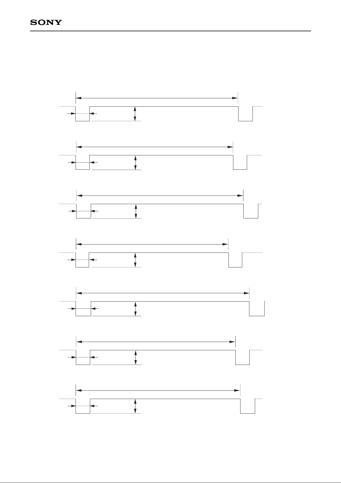
Signals Used for Measurements
SIG-H1
4.8 µs
0.57 V
SIG-H2
61.98 µs
4.65 µs
0.57 V
SIG-H3
65.21 µs
4.96 µs
0.57 V
SIG-H4
59.759 µs
4.51 µs
0.57 V
SIG-H5
67.870 µs
5.13 µs
0.57 V
SIG-H6
62.563 µs
4.73 µs
0.57 V
SIG-H7
64.583 µs
4.88 µs
0.57 V
63.556 µs
f
H=15.734 kHz
f
H+400 Hz
f
H–400 Hz
f
H+1 kHz
f
H–1 kHz
f
H+250 Hz
f
H–250 Hz
H system
Page 21
—21—
CXA1871S
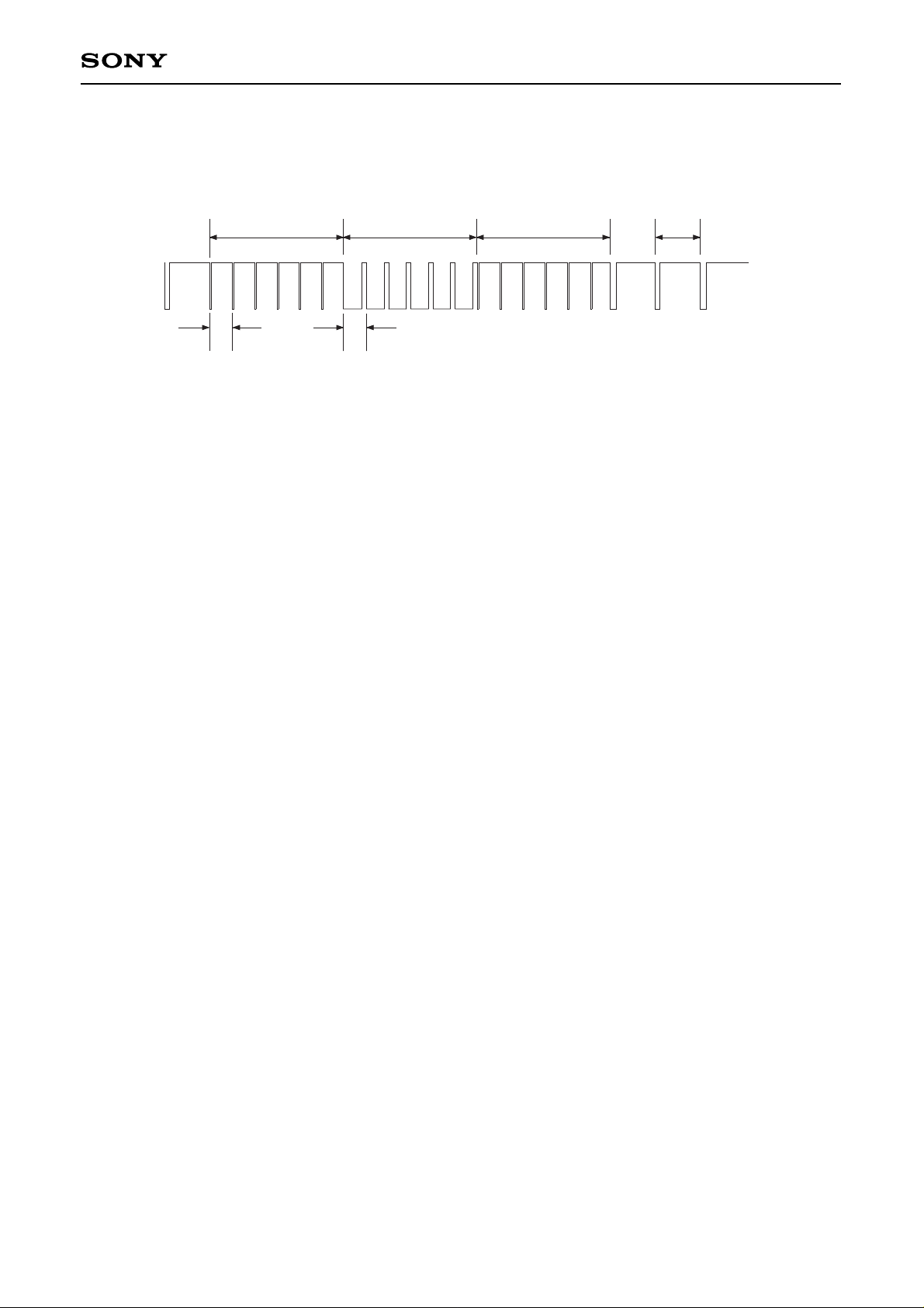
V system
SIG-V1
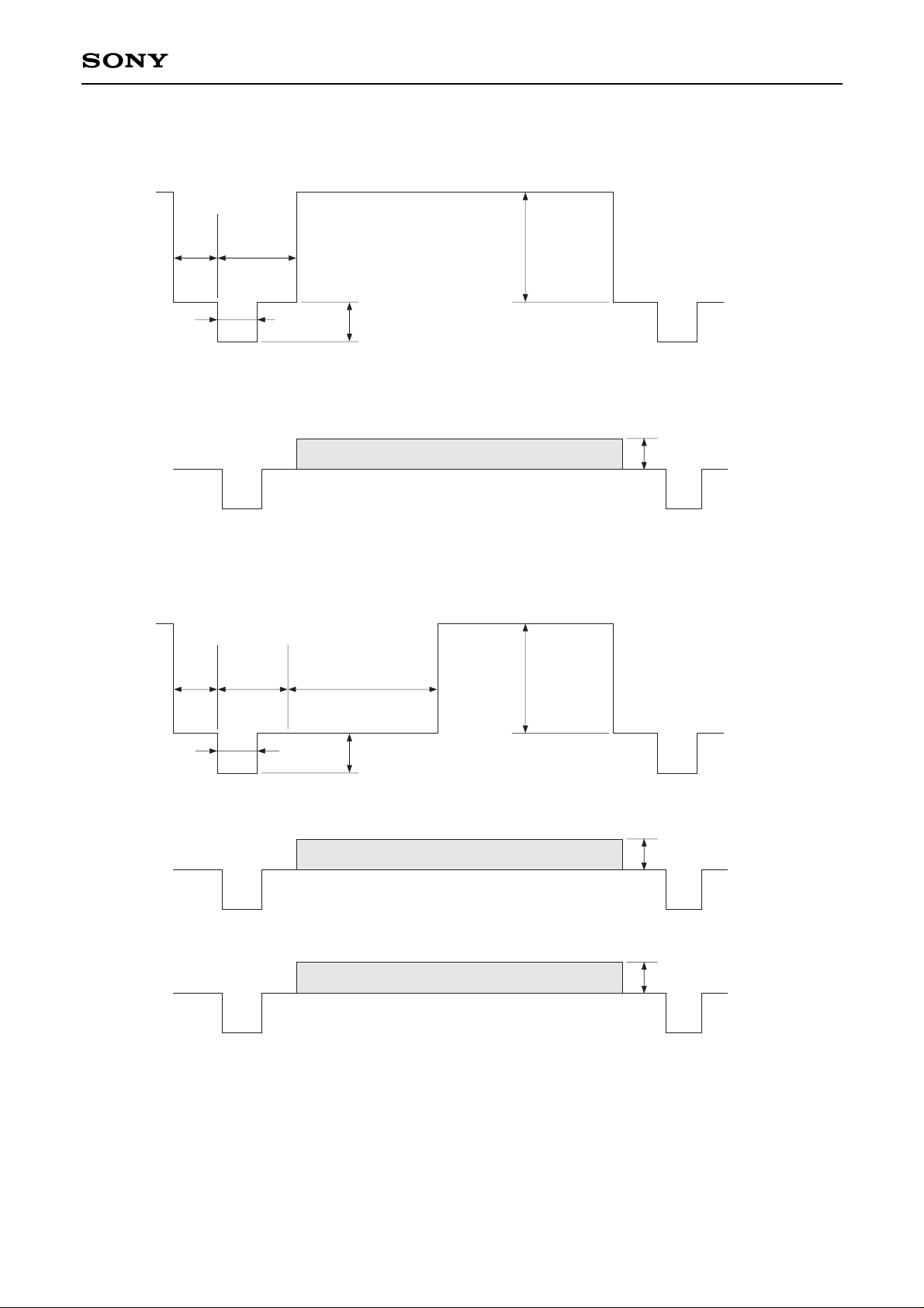
Vsync3 HEquivalent pulse 3 H Equivalent pulse 3 H 1 H=63.556 µs
Equivalent pulse interval 1/ 2 H Vsync interval 1/ 2 H
4.8 µs 2.5 µs
fV = fH / 262
Page 22
—22—
CXA1871S
4.8 µs
9.5 µs1.7 µs
1.7 µs 9.5 µs 26 µs
4.8 µs 0.57 V
1.43 V
0.7 V
0.7 V
0.7 V
f = 100kHz
f = 3MHz
SIG-Y1
SIG-Y2
SIG-Y3
SIG-Y4
SIG-Y5
0.57 V
1.43 V
f = 3.58 MHz
Y system
Page 23

—23—
CXA1871S
0.7V
0.28V
1.4V
0.7V
0.14V
SIG-Y6
SIG-Y7
SIG-Y8
SIG-Y9
SIG-Y10
SIG-Y11
f = 8MHz
f = 5 MHz
f = 5MHz
f = 9 MHz
63.556µs
4.8µs 0.57V
9.8µs6.6µs
1.43V
Page 24

—24—
CXA1871S
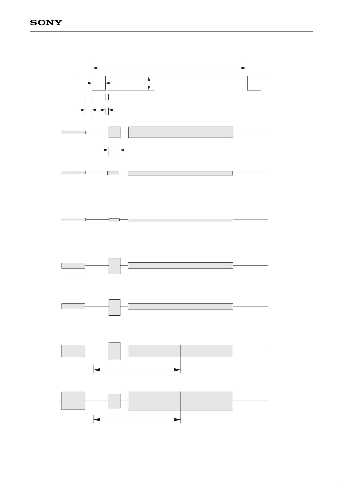
SIG-H1
63.556 µs
4.8 µs
0.57 V
SIG-C2
SIG-C3
SIG-C5
SIG-C1
SIG-C4
1.7 µs
0.5 µs
SIG-C6
3 µs
35.5 µs
fsc+350 Hz
0.5 Vp-p
fsc+100kHz, 0.1 Vp-p
0.5 Vp-p
fsc+100 kHz, 0.1 Vp-p
fsc–350 Hz
0.5 Vp-p
fsc+100 kHz, 0.5 Vp-pfsc
0.5 Vp-p
fsc0°
35.5 µs
0.5 Vp-p
fsc0°
fsc+180°, 0.3 Vp-p
fsc
1 Vp-p
fsc+100 kHz, 1.0 Vp-p
fsc-90°, 0.3 Vp-p
fsc+0°, 0.3 Vp-p
fsc+90°, 0.3 Vp-p
f
H = 15.734 kHz
0 dB
6 dB
C system
Page 25
—25—
CXA1871S
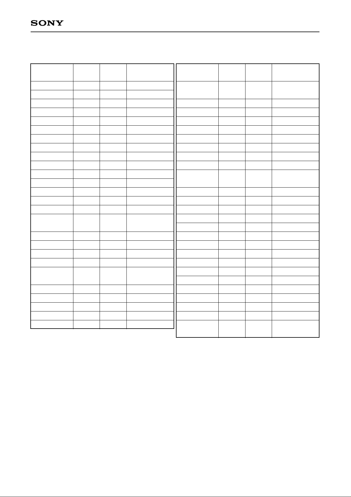
SIG-C10
SIG-C11
SIG-C7
SIG-H1
63.556 µs
4.8 µs
0.57 V
1.7 µs 0.5 µs
SIG-C9
SIG-C8
0.5 Vp-p
fsc+500 kHz, 0.1 Vp-p
fsc
0.5 Vp-p
fsc–500 kHz, 0.1 Vp-p
fsc
3µs
50mVp-p
fsc+100 kHz, 50 mVp-p
fsc
5 mVp-p
fsc+100 kHz, 5 mVp-p
fsc
32 mVp-p
fsc+100 kHz, 32 mVp-p
fsc
–20 dB
–30 dB
–40 dB
fH = 15.734 kHz
SIG-C12
0.5 Vp-p
fsc0°
fsc–13°, 0.96 Vp-p fsc+167°, 0.96 Vp-p
35.5 µs
0.5 Vp-p
fsc+104°, 1.36 Vp-p fsc–76°, 1.36 Vp-p
35.5 µs
SIG-C13
fsc0°
Page 26

—26—
CXA1871S
SIG-R1
0.7 Vp-p
1.43 Vp-p
SIG-R2
3 V or 5 V
SIG-R3
5 V
2.5 V
RGB system
Page 27
—27—
CXA1871S
Mesurement Method
I2C Bus Register Initial Settings
Register name
No. Initial
Description
of bits setting
PICTURE
RGB LIM
HUE
IN SW
COLOR
SW GAIN
BRIGHT
NR ON
SHARPNESS
SUB CONT
SUB HUE
SUB COLOR
SUB BRIGHT
TRAP ON
TOT ON
PIX ON
R ON
G ON
B ON
PRE OVER
AXIS
BLACK
DYCOL OFF
REF
ABL
BLUE
6
2
6
1
6
1
6
1
4
4
4
4
6
1
1
1
1
1
1
3
1
1
1
2
2
1
3 FH
3 H
1 FH
0 H
1 FH
0 H
1 FH
0 H
7 H
7 H
7 H
7 H
1 FH
0 H
0 H
1 H
1 H
1 H
1 H
0 H
0 H
0 H
1 H
1 H
0 H
0 H
Maximum value
Maximum value
Center value
V1 IN selected
Center value
0 dB gain
Center value
NR OFF
Center value
Center value
Center value
Center value
Center value
TRAP OFF
TOT OFF
Picture mute
OFF
R output ON
G output ON
B output ON
Minimum value
NTSC detective
axis
BLACK OFF
DY COL OFF
Center value
Minimum value
BLUE OFF
Register name
No. Initial
Description
of bits setting
OSD
G DRIVE
DC TRAN
B DRIVE
GAMMA
G CUTOFF
B CUTOFF
H PHASE
V ON
V EX OFF
AFC
V SHIFT
HV COMP
V SIZE
C MODE
V LIN
SCORR
SYSTEM1
SYSTEM2
SYSTEM3
SYSTEM4
SYSTEM5
X’TAL PIN
DELAY
4.43X’TAL
EXT COLOR
1
5
3
5
3
4
4
4
1
1
2
5
3
6
1
4
4
1
1
1
2
1
2
2
1
1
0 H
FH
0 H
FH
0 H
7 H
7 H
7 H
1 H
1 H
1 H
FH
3 H
1 FH
0 H
7 H
7 H
1
0
0
0
0
2
0
0
0
Luminance level
small
Center value
Minimum value
Center value
Correction OFF
Center value
Center value
Center value
VD output ON
V sync
expansion OFF
Center value
Center value
Center value
Center value
Countdown ON
Center value
Center value
Fixed mode
60 Hz
60 Hz
NTSC
3.58 MHz
Pin 4
Y Delay 0ns
3.58 MHz x’tal
Identification
switching
Page 28
—28—
CXA1871S
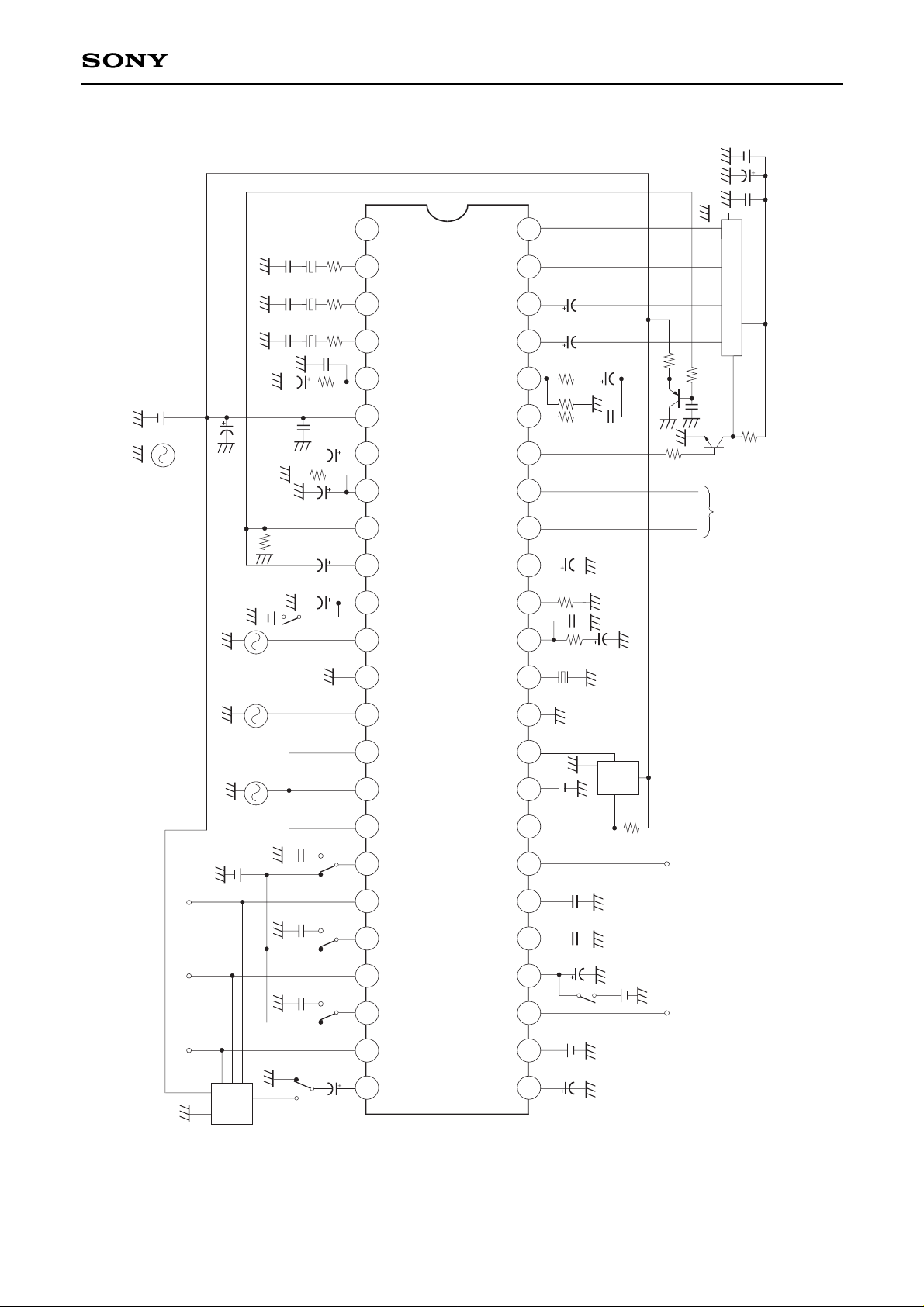
Electrical Characteristics Measurement Circuit
∗
0.01 µ
0.22 µ
2.2 k
4700 p560
0.22 µ film
0.1 µ film
500 kHz
ceramic
oscillator
15 k
0.01 µ
5.6 k
2.2 µ
330
10 k
3.3 k100 p
12 p
2.2 k
C IN
10 µ
CRT
DRIVE
0.22 µ
CXA1871S
∗
∗
∗
2
I C
X RAY 0 V
4.7 µ
9/5 V
VDC 6.7 V
VCC
47 µ
0/6V
25
26
27
28
29
30
31
32
33
34
35
36
37
38
39
40
41
42
46
47
48
43
44
45
HP
GEN.
1 µ
1 µ
1H DELAY LINE
0.01 µ
47 µ
5 V
V2 IN
R-Y OUT
SDA
SCL
V SYNC
H SYNC
R-Y IN
REG
IREF
AFC
CERA
J GND
HP
XRAY
HD
V PLS
V LPF
V OSC
ABL LPF
VD
ABL IN
B-Y OUT
B-Y IN
SCP
X NTSC
V
CC
APC
V1 IN
A PED
Y IN
C IN
V GND
OSD BLK
OSD R
OSD G
OSD B
R S/H
R OUT
G S/H
G OUT
B S/H
B OUT
IK
V HOLD
SW OUT
X PAL2
X PAL1
SECAM REF
12 p
2.2 k
12p
2.2 k
0.47 µ
470 p
15 k
0.47 µ
330 k
0.22 µ
0.47 µ
3/5 V
100 k
9 V
2
3
4
5
6
7
8
9
10
11
12
13
14
15
16
17
18
19
20
21
22
23
1
24
2.2 k
4.7 µ
220 k
1 µ
∗ Pin 18, 20, 22 and 24 switches are
ON only for electrical characteristic
measurements No. 106 to 109.
Page 29
—29—
CXA1871S
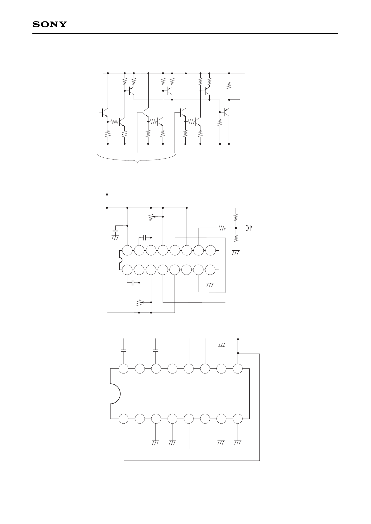
Reference Circuit
+9 V
1.1 k
110 k 1.1 k 110 k1.1 k 110 k
68 k
2SC
2785
2SA
1175
2SA
1175
2SA
1175
2SA1175
GND
2SC
2785
2SC
2785
2SC
2785
2SC
2785
2SC
2785
1 k 470
1 k 470
1 k 470
47 k
100
100
100
from Pins R, G and B OUT of the IC
to IK of the IC
CRT Drive Circuit
+9 V
470 p
6.8 k
1 µ
3.3 k
HD
10 k
6.8 k
Pulse width 12 µ
0.022 µ
HP
Delay 10 µs
1000 p
1 2 3 4 5 6 7 8
910111213141516
4538
10 k
HP Gen
1H DELAY LINE
SCP
TDA4665
R-Y INB-Y INB-Y OUT +5 V
1000 P
R-Y OUT
1000 P
111213141516 10
9
1 2 3 4 5 6 7 8
Page 30
—30—
CXA1871S
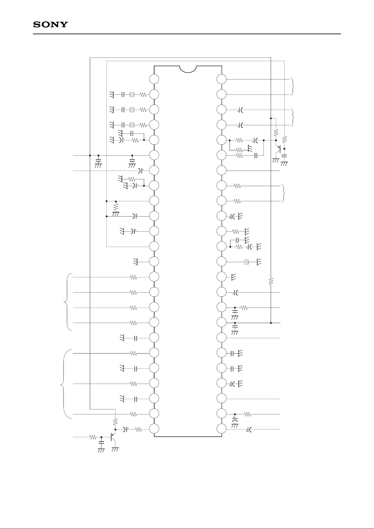
Application Circuit
PAL/N or
4.43 MHz
X'TAL
Composite
video 1 input
OSD
inputs
RGB
outputs
V drive output
V pulse output
H drive output
H pulse input
X-ray protection input
0.1 µ film
ABL input
1 µ
Composite
video 2 input
X NTSC
V
CC
APC
V1 IN
A PED
Y IN
C IN
V GND
OSD BLK
OSD R
OSD G
OSD B
R S/H
R OUT
G S/H
G OUT
B S/H
B OUT
IK
V HOLD
SW OUT
X PAL2
X PAL1
SECAM REF
V2 IN
SDA
SCL
V SYNC
H SYNC
REG
IREF
AFC
CERA
J GND
HP
XRAY
HD
V PLS
V LPF
V OSC
ABL LPF
VD
ABL IN
SCP
R-Y OUT
B-Y OUT
B-Y IN
R-Y IN
Color difference
output to 1 H
delay line
Color difference
input from 1 H
delay line
1 µ
NTSC X'TAL
PAL/M X'TAL
1
2
3
4
5
6
7
8
9
10
11
12
13
14
15
16
17
18
19
20
21
22
23
24
1 µ
10 k
100 p 3.3 k
220
220
0.01 µ
15 k
5.6 k 2.2 µ
10 k
1 µ
1 µ
100 p
0.1 µ film
0.22 µ film
4.7 µ
1.5 k
1 µ
0.22 µ
0.1 µ film
0.1 µ film
12 p
12 p
12 p
470 p
0.47 µ 15 k
47 µ
0.01 µ
0.22 µ
330 k
0.47 µ
0.22 µ
4.7 µ
220
220
220
220
220
220
220
100
0.47 µ
47 k
10 k
47 p
Ik input
2.2 k
+9 V
2
560 4700 p
2.2 k
2.2 k
2.2 k
2.2 k
4.7 µ
25
26
27
28
29
30
31
32
33
34
35
36
37
38
39
40
41
42
43
44
45
46
47
48
I C
330
220 k
∗1 ∗2
Sand Cathle Pulse
output
500 kHz
ceramic
oscillator
∗ When 4.43 MHz XTAL is connected to Pin 2
change the capacitance of +1 to 10 pF and
the resistor of ∗2 to 470 Ω, and then use them.
Application circuits shown are typical examples illustrating the operation of the devices. Sony cannot assume responsibility for
any problems arising out of the use of these circuits or for any infringement of third party patent and other right due to same.
Page 31

—31—
CXA1871S
Description of Operation
1. Synchronizing and picture distortion correction systems
The video signals (2 Vp-p standard) input to Pins 43 and 44 are led to the horizontal and vertical sync
separation circuits for sync separation.
This horizontal sync signal is compared with the signal obtained by 1/32 frequency dividing the 32 fh VCO
output using the ceramic oscillator (frequency: 503.5 kHz) to detect a phase difference. The error voltage
resulting from the phase difference is applied to the H oscillator after attenuating the medium and high
frequency components by a lag-lead filter. The phase of the H oscillator output is compared and shifted to
match the phase of the H deflection pulse (flyback pulse) input from Pin 34, and then output from Pin 32.
After the vertical sync signal is synchronized to the input signal by the V countdown system, a sawtooth
wave is generated by charging and discharging the capacitor attached externally to Pin 29. AGC is
performed to ensure that the amplitude of the sawtooth wave output is maintained constant regardless of
the vertical frequency of the input, after which the sawtooth wave passes through the picture distortion
correction circuit and is output from Pin 27.
Note that there is no need to adjust the free running frequency for either the H or V oscillator.
When voltage of 3 V or more is applied to Pin 33, the H drive output is held at low level. A time constant
circuit is included to protect against overvoltages, and H drive is output normally when high voltage input
continues for less than 7 V cycles. To release holddown, the IC must be turned off and then started up
again.
BGP, HBLK and VBLK are output to Pin 42 as SCP (Sand Cathle Pulse).
Note)
If external capacitance of Pin 30 is used with 0.1 µF or less of the recommended value, vertical sync output
may be unstable.
When changing the capacitance value, use it with 0.047 µF or more.
Page 32

—32—
CXA1871S
2. Y/C system
The Y/C system has the following three input systems.
Composite video input (1 Vp-p/2 Vp-p) → 2 systems (The gain can be switched between 0 and 6 dB for
both systems.)
Y/C separation input (2 Vp-p) → 1 system
The Y signal (specified input level 2 Vp-p) input to Pin 10 is passed through the sub-contrast control,
chroma trap (or delay line), delay line, sharpness control, noise reduction, clamp and auto pedestal circuits.
The signal is then mixed with the color difference signal, passed through the clamp and Y/C MIX circuits
again, and input to the RGB interface system block.
Since a built-in chroma trap is provided, the video signal can be directly input. Trap frequency adjustment
is not necessary as a dummy filter is provided inside the IC and feedback is applied using the 3.58 MHz or
4.43 MHz signal generated by a crystal oscillator for reference. When the chroma trap is off, the Y system
frequency response is approximately 8 MHz, –3 dB for R, G and B outputs.
Sharpness control is delay line type with a variable PRE/OVER ratio.
Dynamic picture control consists of pulling in the signal below 40 IRE to the black side so that the signal
black peak held by Pin 11 becomes the pedestal level.
The chroma signal (specified input level, burst 570 mVp-p, or video signal 2 Vp-p) input to Pin 12 is passed
through the ACC and TOT, and the burst only is set to the maximum gain by the B.G. This burst is then
peak detected by ACC DET, level controlled by the I2C bus register, and fed back to the ACC again. When
the B.G. output burst signal is smaller than a certain level, killer turns on, the chroma signal is replaced with
DC by the B.G., and the color gain is set to the minimum. The burst signal is detected using the VCO
oscillation output which has received hue control as the carrier, and a signal (the R-Y axis sub-carrier due
to chroma demodulation) whose phase is offset 90° from the burst signal is generated. During PAL input,
this sub-carrier is inverted 180° every 1 H and output. The phase is not inverted during NTSC input. The
chroma signal is demodulated into the color difference signals R-Y and B-Y by this sub-carrier. The signal
is set to 6 dB during NTSC input, or passed through the 1 H delay line and set to 0 dB during SECAM and
PAL input, after which it is input to the matrix circuit where the G-Y color difference signal is generated.
Then, the color difference signals are passed through the Y/C MIX circuit, and input together with the Y
signal to the RGB interface system block.
The detective axis (NTSC/PAL) can be switched by the I2C bus register.
NTSC or PAL input is automatically identified and output to the status register. In addition, during PAL
input, the phase relationship between the burst and R-Y sub-carrier is detected. If a phase error is detected
at this time, it is corrected by applying feedback to the flip flop.
Page 33

—33—
CXA1871S
3. RGB interface system
YS/YM switching is performed according to the amplitude of the OSD RGB input blanking signal input from
Pin 14.
0 to 1.5 V → TV (Y/C input)
1.5 to 3.5 V → TV –6 dB
3.5 to 5.5 V → Black
The R, G and B signals of the Y/C system pass through the RGB switch (BLUE and BLACK ON/OFF) and
receive picture control. These signals are mixed with the digital R, G and B signals (specified input level 0
to 5 V DC) input from Pins 15, 16 and 17, passed through the dynamic color, gamma correction, bright
control, drive adjustment (R channel is fixed, G and B channels are variable.), cut-off adjustment (R channel
is fixed, G and B channels are variable.) and auto cut-off DC level shift circuits, and then output from Pins
19, 21 and 23 as the R, G and B signals. The RGB output amplitude has a limit voltage whose setting
value can be controlled with the I2C bus register. The digital R, G and B signals are mainly used for on
screen display of channels, etc. and the display level can be set with the I2C bus register.
The signal input to Pin 26 (ABL IN) is compared with the internal reference voltage and is then integrated by
the capacitor connected to Pin 28 (ABL LPF) for picture and brightness control. Picture ABL mode and
combined picture ABL and brightness ABL mode can be switched with the I2C bus register.
Note)
When the digital R, G and B signals and OSDBLK signal are not used, connect Pins 14, 15, 16 and 17 to
GND.
Auto cut-off
For white balance, drive control (gain control between R, G and B outputs) and cut-off control (black side
DC level control) are involved. This IC uses the I2C bus register for drive control. For cut-off control, a loop
is formed between the IC and CRT to achieve auto cut-off control.
This auto cut-off arrangement makes it possible to compensate for CRT changes with time. To absorb the
CRT variance, the cut-off voltages of the G and B outputs are adjusted by the I2C bus register.
The auto cut-off loop is configured as described below.
(1) R, G and B reference pulses for auto cut-off, shifted 1H each in the order mentioned, are added to
the top of the picture.
(2) The IK of each of the R, G and B outputs is converted to a voltage and input to Pin 24.
(3) The voltage input to Pin 24 is compared with the reference voltage in the IC to change the DC level
of the reference pulses.
The loop mentioned above determines the shift level of the R, G and B outputs and lets the capacitances
connected to Pins 18, 20 and 22 hold the DC shift level during the 1 V period. If the voltage at any one of
Pins 18, 20 and 22 is less than 4.2 V, the status register IK (bit 6) becomes “1”. Use this information to
blank the R, G and B outputs with the I2C bus register. The positions of the reference pulses can be
changed by the I2C bus register.
Page 34

—34—
CXA1871S
fSC fH fV
PIN
NO.
4433619 15625 50
4.43/PAL
[Hz] [Hz] [Hz]
4406250 15625 50
Pin 2
SECAM 4250000 [Hz] [Hz]
[Hz]
4.43 4433619 15734 60
NTSC [Hz] [Hz] [Hz]
3575611 15734 60
Pin 3PAL/M
[Hz] [Hz] [Hz]
3579545 15734 60
NTSC
[Hz] [Hz] [Hz]
Pin 4
System Identification Method (when 443XTAL = 0)
Conditions for releasing the lock
(1)KILLER=ON
(2)When NT/PAL identification
result changes from PAL to
NTSC∗
2
(1)KILLER=ON
(2)When NT/PAL identification
result changes from PAL to
NTSC∗
2
(3)When 50/60 identification
result changes from 60 to 50
(1)KILLER=ON
(2)When 50/60 identification
result changes from 60 to 50
Conditions for locking the
system to this pin
(1)KILLER=ON
(2)50/60 identification result
= 50 Hz∗
1
(1)KILLER=OFF
(1)KILLER=OFF
fSC fH fV
PIN
NO.
3582056 15625 50
PAL/N
[Hz] [Hz] [Hz]
Pin 2
3575611 15734 60
PAL/M
[Hz] [Hz] [Hz]
Pin 3
3579545 15734 60
NTSC
[Hz] [Hz] [Hz]
Pin 4
∗1When the 50/60 identification result changes from 60 Hz to 50 Hz, pin switching is performed until the
system is locked to Pin 2. However, when the 50/60 identification result changes from 50 Hz to 60 Hz,
identification is ignored.
∗2NTSC→PAL = Don’t care
System Identification Method (when 443XTAL = 1)
Conditions for releasing the lock
(1)KILLER=ON
(2)When NT/PAL identification
result changes from PAL to
NTSC∗
2
(1)When any one of the
conditions to the left is not
met
(1)KILLER=ON
(1)KILLER=ON
(2)When NT/PAL identification
result changes from PAL to
NTSC∗
2
(3)When 50/60 identification
result changes from 60 to 50
(1)KILLER=ON
(2) When 50/60 identification
result changes from 60 to 50
Conditions for locking the
system to this pin
(1)KILLER=ON
(2)50/60 identification result
= 50 Hz∗
1
(1)KILLER=ON
(2)50/60 identification result
= 50 Hz∗
1
(3)SECAM ID=ON
(1)KILLER=OFF
(1)KILLER=OFF
(1)KILLER=OFF
∗1When the 50/60 identification result changes from 60 Hz to 50 Hz, pin switching is performed until the
system is locked to Pin 2. However, when the 50/60 identification result changes from 50 Hz to 60 Hz,
identification is ignored.
∗2NTSC→PAL = Don’t care
Page 35
—35—
CXA1871S
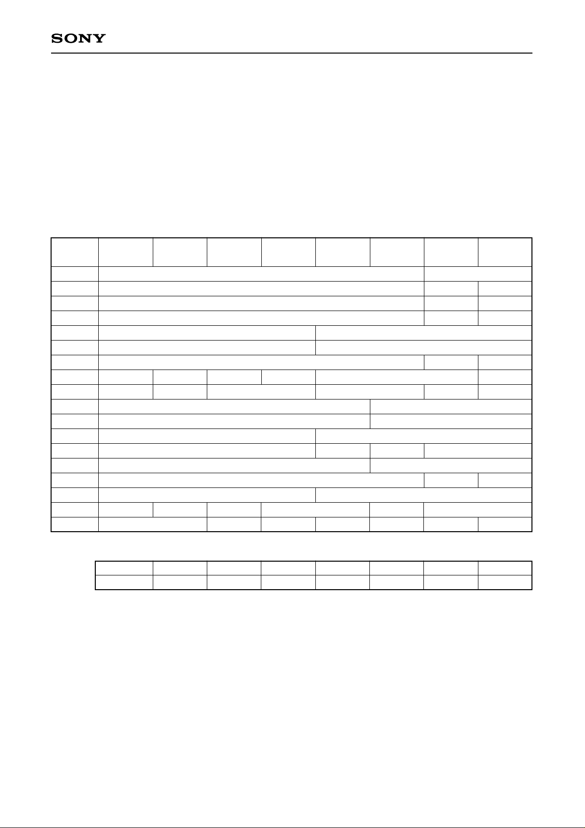
Definition of I2C Bus Registers
Slave addresses
88H: Slave Receiver
89H: Slave Transmitter
Register table
• All registers are set to 0 when the IC power is turned on.
• “X” indicates “don’t care”; “∗” indicates undefined.
Control registers
bit 3 bit 2 bit 1 bit 0
RGB LIM
∗ IN SW
∗ SW GAIN
∗ NR ON
SUB CONT
SUB COLOR
TRAP ON TOT ON
PRE OVER AXIS
ABL BLUE OSD
DC TRAN
GAMMA
B CUTOFF
V ON VEX OFF AFC
HV COMP
0 C MODE
S CORR
SYSTEM5 X’TAL PIN
∗ ∗ ∗ ∗
bit 7 bit 6 bit 5 bit 4
PICTURE
HUE
COLOR
BRIGHT
SHARPNESS
SUB HUE
SUB BRIGHT
PIX ON R ON G ON B ON
BLACK DY COL OFF REF
G DRIVE
B DRIVE
G CUTOFF
H PHASE
VSHIFT
V SIZE
V LIN
SYSTEM1 SYSTEM2 SYSTEM3
DELAY 4.43X’TAL EXT COLOR
Sub
Address
XXX00000
XXX00001
XXX00010
XXX00011
XXX00100
XXX00101
XXX00110
XXX00111
XXX01000
XXX01001
XXX01010
XXX01011
XXX01100
XXX01101
XXX01110
XXX01111
XXX10000
XXX10001
bit 7 bit 6 bit 5 bit 4 bit 3 bit 2 bit 1 bit0
H LOCK IK KILLER XRAY NT/PAL 50/60 VCO-F SECAM
Status register
SYSTEM4
Page 36

—36—
CXA1871S
Description of I2C Bus Registers
PICTURE (6) Picture control
0 = Minimum
63 = Maximum
RGB LIM (2) RGB output amplitude limiter voltage control
0 = Limited at 4.9 V (with a black level of 2 V)
1 = Limited at 5.1 V (with a black level of 2 V)
2 = Limited at 5.3 V (with a black level of 2 V)
3 = Limited at 5.5 V (with a black level of 2 V)
HUE (6) Hue control
0 = Skin color nearer to red
63 = Skin color nearer to green
IN SW (1) Input selector switch
0 = V1 IN
1 = V2 IN
COLOR (6) Color control
0 = Minimum
63 = Maximum
SW GAIN (1) SW output gain switching
0 = SW GAIN 0dB
1 = SW GAIN 6dB
BRIGHT (6) Brightness control
0 = Minimum
63 = Maximum
NR ON (1) Y signal noise reduction ON/OFF
0 = OFF
1 = ON
SHARPNESS (4) Sharpness control
0 = Minimum
15 = Maximum
SUB CONT (4) Sub-contrast control
0 = Minimum
15 = Maximum
Sub Address
00000
Sub Address
00001
Sub Address
00010
Sub Address
00011
Sub Address
00100
Page 37

—37—
CXA1871S
SUB HUE (4) Hue center control
0 = Skin color nearer to red
15 = Skin color nearer to green
SUB COLOR (4) Color center control
0 = Minimum
15 = Maximum
SUB BRIGHT (6) Sub-bright control
0 = Minimum
63 = Maximum
TRAP ON(1) Chroma trap in Y system ON/OFF
0 = OFF
1 = ON
TOT ON (1) Chroma TOT filter ON/OFF
0 = OFF
1 = ON
PIX ON (1) Picture mute ON/OFF
0 = Picture mute (Auto cut-off reference pulse also muted.)
1 = Picture mute released.
R ON (1) R OUT ON/OFF
0 = R OUT OFF
1 = R OUT ON
G ON (1) G OUT ON/OFF
0 = G OUT OFF
1 = G OUT ON
B ON (1) B OUT ON/OFF
0 = B OUT OFF
1 = B OUT ON
PRE OVER (3) Sets the sharpness preshoot and overshoot ratio.
0 = Pre Shoot 100 %, Over shoot 0 %
7 = Pre Shoot 25 %, Over shoot 75 %
AXIS(1) Detective axis switching
0 = NTSC
1 = PAL
Sub Address
00101
Sub Address
00110
Sub Address
00111
Page 38

—38—
CXA1871S
BLACK (1) Blanks the Y IN/C IN signals and sets the R, G and B outputs to black
level.
0 = OFF
1 = ON
DY COL OFF (1) Dynamic color ON/OFF
0 = Dynamic color ON
1 = Dynamic color OFF
REF (2) Switches the auto cut-off reference pulse position.
0 = B-18H G-19H R-20H
1 = B-20H G-21H R-22H
2 = B-22H G-23H R-24H
3 = B-24H G-25H R-26H
ABL (2) ABL mode setting
0 = Picture ABL mode (including protective bright ABL)
1 = Combined picture ABL and bright ABL mode (bright ABL low)
2 = Combined picture ABL and bright ABL mode (bright ABL medium)
3 = Combined picture ABL and bright ABL mode (bright ABL high)
BLUE (1) On screen display B IN ON/OFF. Setting to ON turns the entire screen
BLUE.
0 = OFF
1 = ON
OSD (1) On screen display luminance setting
0 = Level small
1 = Level large
G DRIVE (5) G OUT drive control
0 = Minimum
31 = Maximum
DC TRAN (3) DC transmission ratio setting
0 = Maximum (100 %)
7 = Minimum (75 %)
B DRIVE (5) B OUT drive control
0 = Minimum
31 = Maximum
GAMMA (3) γcorrection value setting
0 = Correction OFF
7 = Maximum correction
Sub Address
01000
Sub Address
01001
Sub Address
01010
Page 39

—39—
CXA1871S
G CUTOFF (4) G OUT cut-off voltage control
0 = Minimum
15 = Maximum
B CUTOFF (4) B OUT cut-off voltage control
0 = Minimum
15 = Maximum
HPHASE (4) Horizontal position control
0 = Screen shifted to right
15 = Screen shifted to left
V ON(1) VD output ON/OFF
0 = VD output stopped. (Picture mute applied simultaneously. Auto cut-off reference
pulse also muted.)
1 = VD output
V EX OFF (1) V sync expansion ON/OFF
0 = V sync expansion ON
1 = V sync expansion OFF
AFC (2) AFC loop gain switching
0 = AFC loop gain large
1 = AFC loop gain medium
2 = AFC loop gain small
3 = AFC loop open, free running mode
V SHIFT (5) Vertical position control
0 = Rise
31 = Lower
HV COMP (3) Vertical correction amount setting for high voltage fluctuations
0 = Correction amount minimum
7 = Correction amount maximum
V SIZE (6) Vertical amplitude control
0 = V size minimum
63 = V size maximum
C MODE (1) V countdown system mode switching
0 = Non-standard signal mode, standard signal mode and no signal mode switched
automatically.
1 = Fixed to non-standard signal mode (wide V sync window mode).
Sub Address
01011
Sub Address
01100
Sub Address
01101
Sub Address
01110
Page 40

—40—
CXA1871S
V LIN (4) Vertical linearity control
0 = Top of screen compressed, bottom of screen expanded.
15 = Top of screen expanded, bottom of screen compressed.
S CORR (4) Vertical S correction control
0 = S correction amount minimum
15 = S correction amount maximum
Sub Address
01111
Page 41

—41—
CXA1871S
SYSTEM1(1) Selects the internal mode switching method.
0 = Automatic switching
1 = Fixed according to the bus data
(When ∗1 is selected, the SYSTEM3 to 5 and X’TAL PIN registers below must be
designated.)
SYSTEM2 (1) Selects the V cycle when sync cannot be obtained if automatic switching
is selected by SYSTEM1.
0 = Outputs 60 Hz pulses when sync cannot be obtained.
1 = Outputs 50 Hz pulses when sync cannot be obtained.
SYSTEM3(1) Selects the V cycle.
0 = 60 Hz
1 = 50 Hz
SYSTEM4 (2) Inputs the input signal broadcast system.
0 = NTSC
1 = PAL
2 = SECAM
3 = SECAM
SYSTEM5 (1) Selects the VCO frequency
0 = 3.58 MHz
1 = 4.43 MHz
X'TAL PIN (2) Selects which of the crystals connected to the various pins to use.
0 = Pin 2
1 = Pin 3
2 = Pin 4
3 = Pin 4
4.43X'TAL (1) Inputs whether the crystal connected to Pin 2 is 3.58 MHz or 4.43 MHz.
(When connecting a 4.43 MHz crystal, be sure to connect it to Pin 2.)
0 = 3.58 MHz
1 = 4.43 MHz
EXT COLOR (1) Forcibly switches the DET SW input to external input (R-Y IN, B-Y IN).
0 = Switched according to the NTSC/PAL identification results
1 = External input
DELAY (2) Allows the following delay times to be added to the Y signal.
0 = 0 ns
1 = 40 ns
2 = 80 ns
3 = 120 ns
Sub Address
10000
Sub Address
10001
Page 42

—42—
CXA1871S
H LOCK (1) Returns whether the H oscillator of the IC and the signal input to H SYNC are locked.
0 = Not locked
1 = Locked
IK (1) Returns the AKB loop stable status by detecting the IK current.
0 = IK current stable for each of R, G and B
1 = IK current unstable
KILLER (1) Returns the color killer ON/OFF status.
0 = OFF
1 = ON
XRAY(1) Returns the X-ray protection status.
0 = OFF (X-ray protection is not functioning.)
1 = ON (X-ray protection is functioning.)
NT/PAL (1) Identifies whether the input signal is NTSC or PAL and returns the results.
0 = NTSC
1 = PAL
50/60 (1) Returns the 50/60 Hz identification results.
0 = 60 Hz
1 = 50 Hz
VCO-F (1) Detects the burst frequency of the input signal and returns the results.
0 = 3.58 MHz
1 = 4.43 MHz
SECAM (1) Identifies whether the input signal is SECAM or a different signal and returns the results.
Page 43
—43—
CXA1871S
1 2 3 4 5 6 7 8
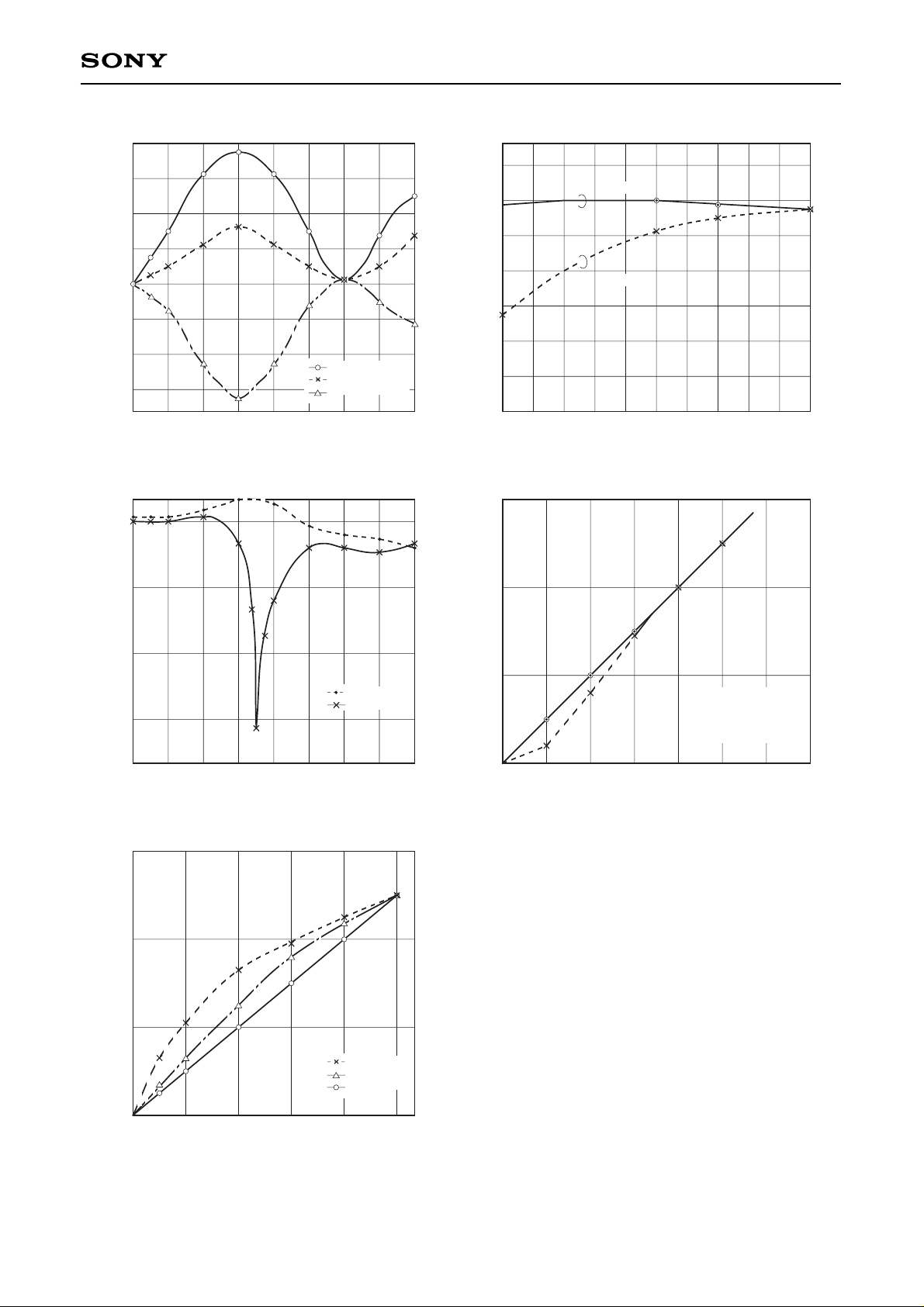
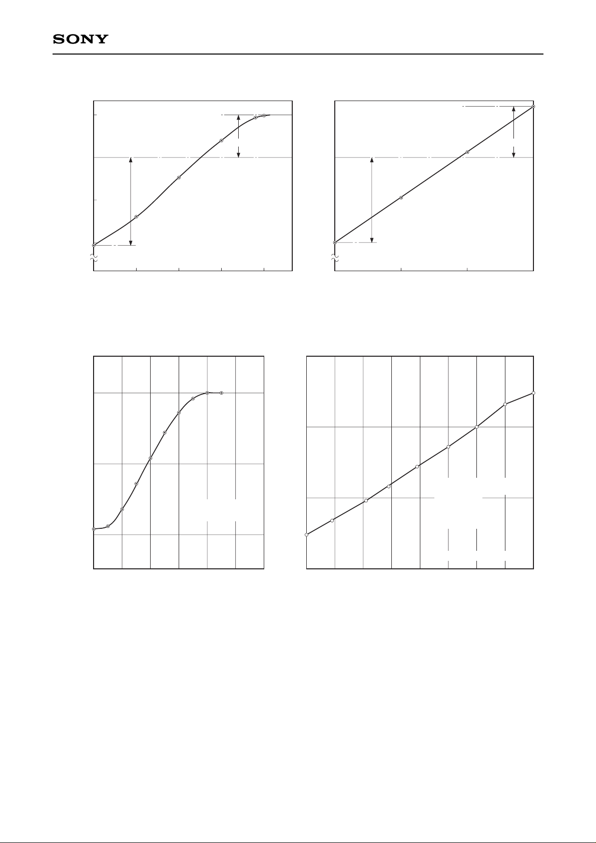
Fig 1. Sharpness characteristics
Attenuation (dB)
0
–2.0
–4.0
–6.0
2.0
4.0
6.0
8.0
0
Fig 2. Chroma frequency characteristics
(dB)
–6.0
–8.0
–10.0
–4.0
–2.0
0
2.0
–800 –600 –400 –200 0 200 400 600 800
1 2 3 4 5 6 7 8
Fig 3. Trap F0 frequency characteristics
Attenuation (dB)
0
–30
0
–20
–10
TRAPSW = 0
TRAPSW = 1
10 20 30 40 50 60
Fig 4. Auto pedestal characteristics
Output amplitude (black to white) (Vp-p)
0.5
0
1.0
Frequency
(MHz)
Input
amplitude
(IRE)
Fig 5. Gamma characteristics
Output amplitude (Vp-p)
Input
amplitude
(IRE)
20 40 60 80 1000
2.0
1.0
GAMMA = 7
GAMMA = 3
GAMMA = 0
SHARPNESS = F
SHARPNESS = 7
SHARPNESS = 0
TOT SW = 1
TOT SW = 0
∆fsc (kHz)
fsc = 3.58MHz
Input
frequency
(MHz)
Input: IRE changed at Full Flat
Output: R OUT
DYCOL= AKB=OFF
GAMMA=DCTRAN=0
Page 44
—44—
CXA1871S
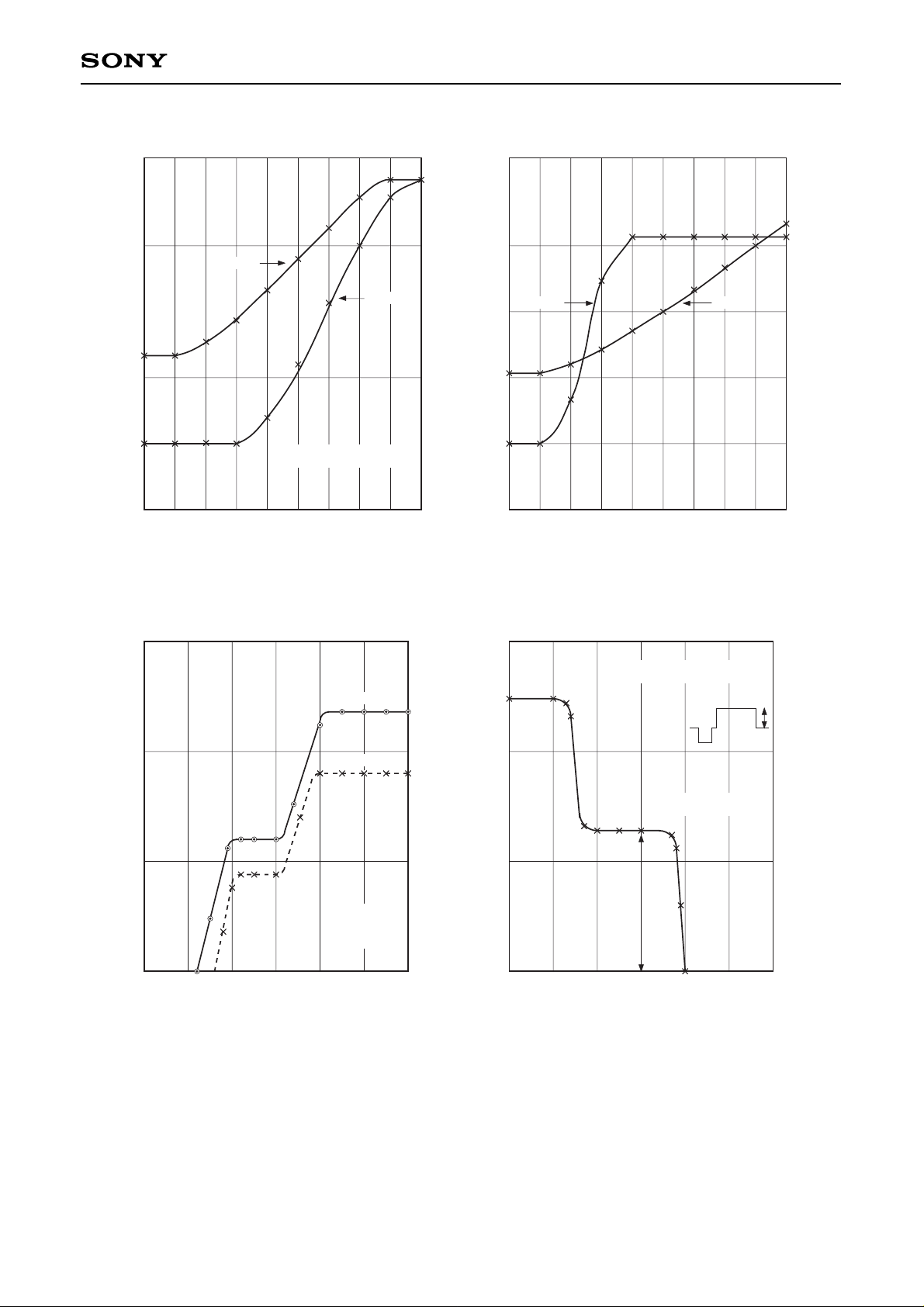
Fig 7. Cutoff control characteristics
IK level (Vp-p)
0.5
1.0
0 5 A F
1.3
VD-output amplitude (Vp-p)
1.35
1.4
8 10 18 20 28 30
1.0
Fig 9. Picture control data (HEX)
Output amplitude (black to white) (Vp-p)
0
2.0
2 4 6 8 10
Fig 8. HV COMP characteristics
0
7 F
Fig 6. G, B drive characteristics
Output amplitude (black to white) (Vp-p)
0
3.0
G, B
drive data
(HEX)
17 1F
2.5
2.0
1.5
Rch = 0.86 Vp-p
3.0
38 3F
ABL IN
Applied
voltage (V)
Variable range 14.7dB
Gch = Bch = –4.5dB
Gch = Bch = +1.5dB
Input: Y IN 1.4Vp-p (black to white)
Output: adjust to be 2.5Vp-p at R OUT
DYCOL = AKB = OFF
DCTRAN = 0
–8.3dB
+3.0dB
Input: Y IN all black
AKB = ON
Output: IK (Pin 21)
G, B
cutoff data
(HEX)
Output: VD (Pin 24)
HV COMP = 7
Input: YIN 1.4Vp-p (black to white)
Output: ROUT
SUBCONT = 7
DYCOL = AKB = OFF
DCTRAN = 0
Page 45
—45—
CXA1871S
Fig 11. ABL characteristics (bright)
Output black lebel (V)
1.0
1.6
0
1.0
Output level (Vp-p
2.0
3.0
1.0 2.0 3.0 4.0 5.0
1.0
Fig 13. OSD-BLK voltage
Output amplitude (black to white) (Vp-p
0
2.0
1 2 3 4 5
Fig 12. OSD RGB I/O characteristics
0
1 2
Fig 10. ABL characteristics (picture)
Output amplitude (white to black) (Vp-p)
0 3 4
2.0
1.0
3.0
6
5 6 7 8 9
ABL-FIL
applied voltage (V)
1 2 3 4 5 6 7 8 9
1.2
1.4
ABL=0
OSDR
applied voltage (V)
OSD = 1
OSD = 0
OSD-BLK
applied voltage (V)
ABL=0
ABL-FIL
applied voltage (V)
Input OSDR
Output ROUT
100IRE = 2.5Vp-p
Input YIN 1.4Vp-p (black to white)
Output R
OUT
PIC = 3F SUBCONT = 7
AKB = OFF
–5.7dB
Input YIN 1.4Vp-p (black to white)
Output R
OUT
ABL=3
ABL=3
Page 46
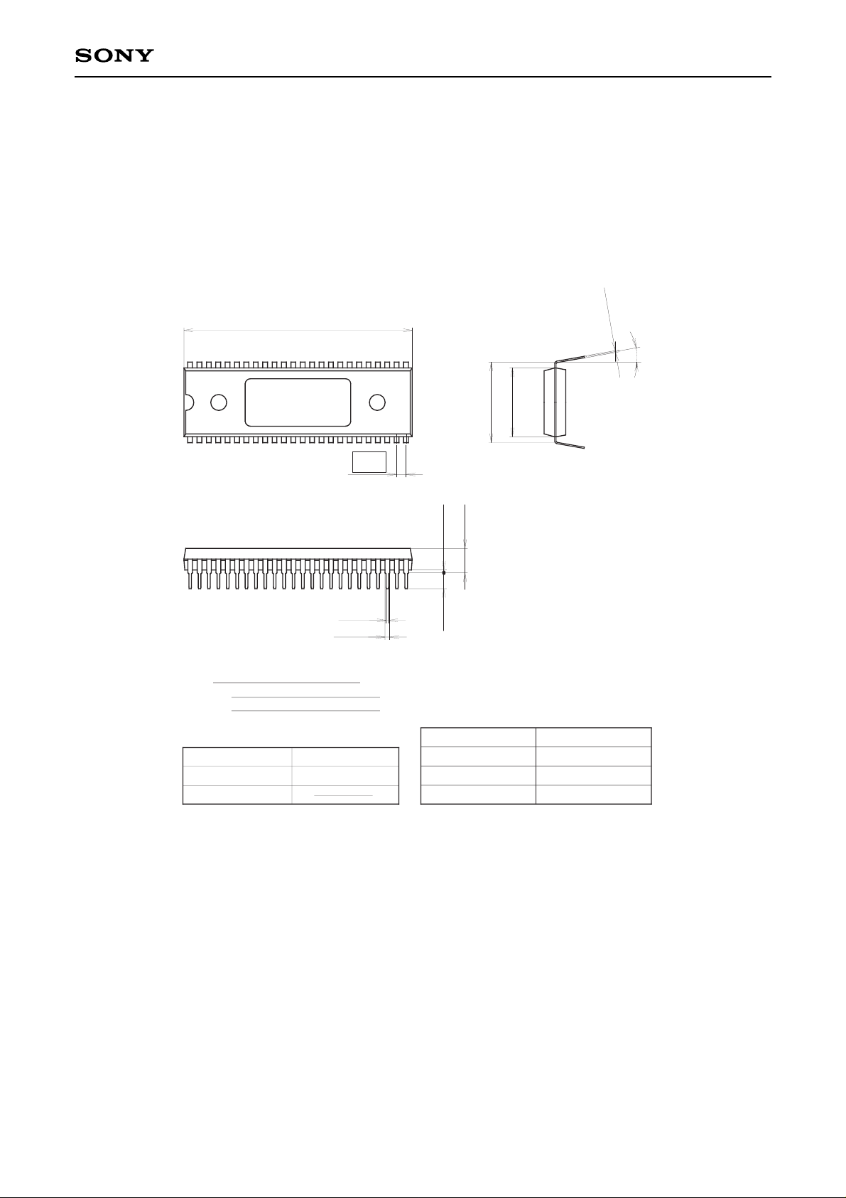
48PIN SDIP (PLASTIC)
13.0
+ 0.3
– 0.1
4.6
+ 0.4
– 0.1
0.25
+ 0.1
– 0.05
48 25
1 24
1.778
15.24
0° to 15°
0.5 ± 0.1
0.9 ± 0.15
3.0 MIN 0.5 MIN
SONY CODE
EIAJ CODE
JEDEC CODE
PACKAGE STRUCTURE
PACKAGE MATERIAL
LEAD TREATMENT
LEAD MATERIAL
PACKAGE MASS
EPOXY RESIN
PLATING
42/COPPER ALLOY
5.1g
SDIP-48P-02
SDIP048-P-0600
43.2
+ 0.4
– 0.1
SOLDER/PALLADIUM
1.All mat surface type.
Two kinds of package surface:
2.Center part is mirror surface.
Package Outline Unit : mm
CXA1871S
—46—
 Loading...