

Page 1

RGB Driver for LCD
Description
The CXA1853AQ is an RGB driver for LCD panels.
It supports a line alternative RGB drive system.
Features
• Built-in RGB signal phase matching sample-and-
hold circuit
• Effective frequency response (18MHz Typ.)
• Built-in gain and breakpoint variable 2-point γ
compensation circuit
• Built-in side black generation circuit for 4:3/16:9
aspect conversion
• Built-in VCOM voltage output circuit
Structure
Bipolar silicon monolithic IC
Applications
• Liquid crystal projectors
• Liquid crystal viewfinders
• Compact liquid crystal monitors
CXA1853AQ
80 pin QFP (Plastic)
Absolute Maximum Ratings (Ta = 25°C)
• Supply voltage VCC16 V
VCC215 V
•Input pin voltage VIN VCC1V
•Operating temperature Topr –25 to +75 °C
• Storage temperature Tstg –55 to +150 °C
• Allowable power dissipation
PD 1500 mW
Operating Conditions
• Supply voltage VCC1 4.75 to 5.25 V
VCC2 11.0 to 14.0 V
• RGB input signal voltage
VIN 0.7 Vp-p
Note)
Note) Defined as the amplitude from the pedestal
level to white.
Sony reserves the right to change products and specifications without prior notice. This information does not convey any license by
any implication or otherwise under any patents or other right. Application circuits shown, if any, are typical examples illustrating the
operation of the devices. Sony cannot assume responsibility for any problems arising out of the use of these circuits.
– 1 –
E96334-PS
Page 2
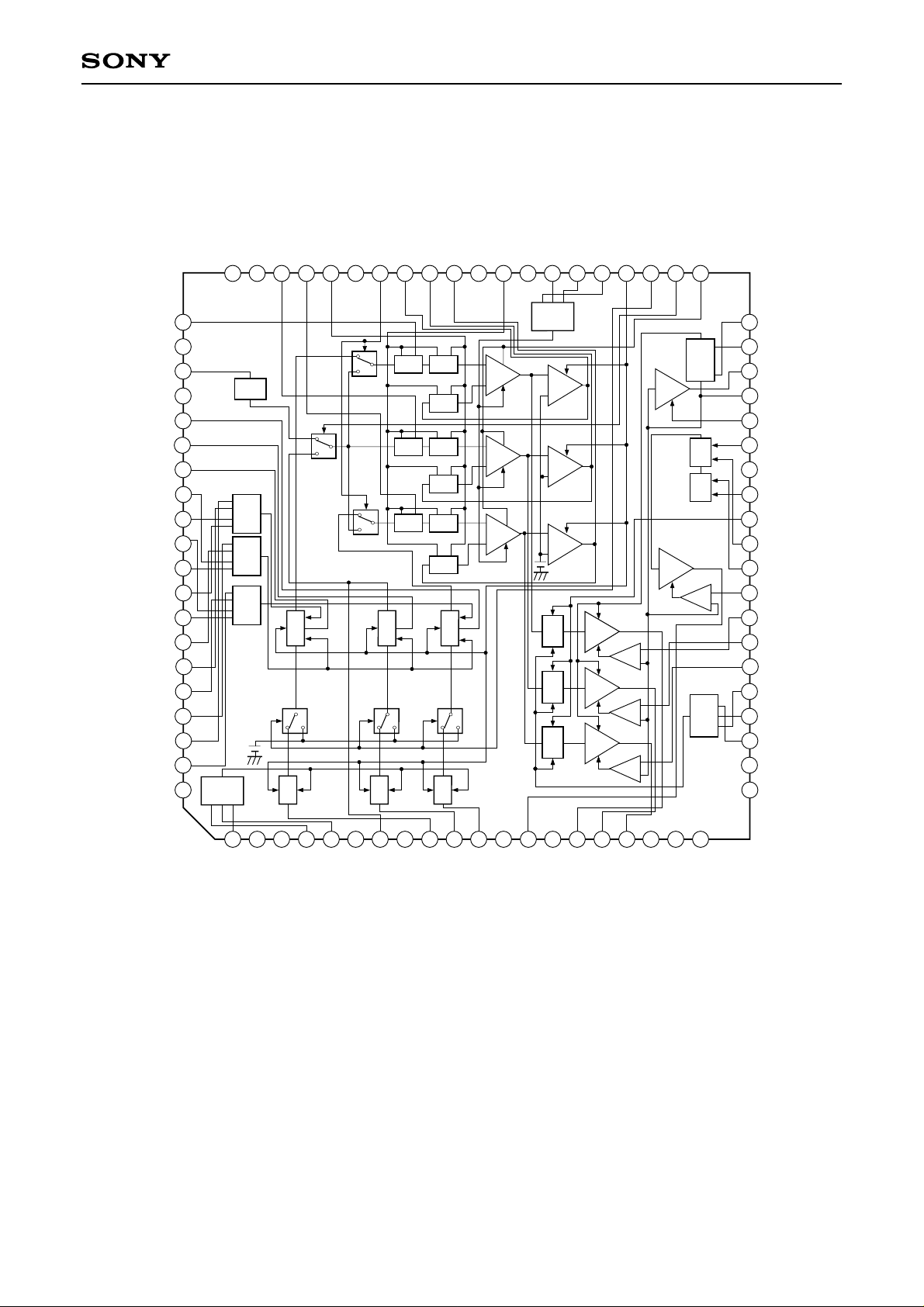
Block Diagram
CXA1853AQ
4
N.C.
SH2
SH3
SH4
N.C.
60
59
57
58
GND
55
56
SIG SEL
54
GCA DETR
53
52
GCA DETG
GCA DETB
50
51
CC
V
IREF
49
48
GND
B GAIN
47
R GAIN
46
RGB GAIN
45
44
XCLP1
43
XCLP2
WHT LIM
GAM SEL
4142
SH1
PV
SH IN
GND
B CLAMP
G CLAMP
R CLAMP
RGB GAM GAIN1
R GAM GAIN1
B GAM GAIN1
RGB GAM GAIN2
R GAM GAIN2
B GAM GAIN2
RGB GAM CTR2
R GAM CTR2
B GAM CTR2
RGB GAM CTR1
R GAM CTR1
B GAM CTR1
N.C.
61
62
CC
S/H
γ AMP
S/HS/H
S/H
S/HS/H
S/H
S/H
S/H
GCA
GCA
GCA
γ AMP
CLP
63
BRT
CONT
CLP
R γ
RGB γ
B γ
CONT
CONT
CONT
CLP
γ AMP
CLP
64
65
66
67
68
69
70
71
72
73
74
75
76
77
78
79
80
GAIN
CONT
EA
EA
EA
SW
SW
SW
BUFFSW
BUFF
BUFF
BUFF
BUFF
BUFF
CTRL
BLKLMT
PRG
SID
SBRT
CONT
40
BLK CENT
39
BLK LIM
38
VCOM OUT
37
SIG CENT CTR
36
VCOM CTR
35
PRG
34
GND
33
SID FRP
32
FRP
31
PRG CTR
30
SID CTR
29
SID CLP
28
R CLP
27
G CLP
26
B CLP
25
R SBRT
B SBRT
24
23
RGB SBRT
GND
22
N.C.
21
1
2
N.C.
RGB MBRT
3
N.C.
4
R MBRT
5
B MBRT
6
N.C.
8
7
GAM OUT
BIN
12
GND
13
SID OUT
14 15
2
CC
V
16
R OUT
17
G OUT
9
10
RIN
11
GIN
1
CC
V
18
B OUT
19
20
3
CC
N.C.
V
N.C.
– 2 –
Page 3
CXA1853AQ
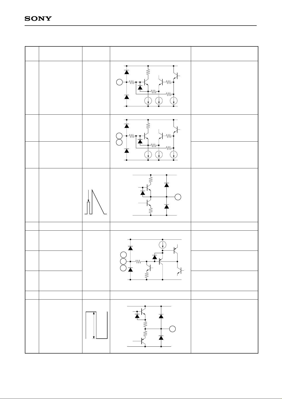
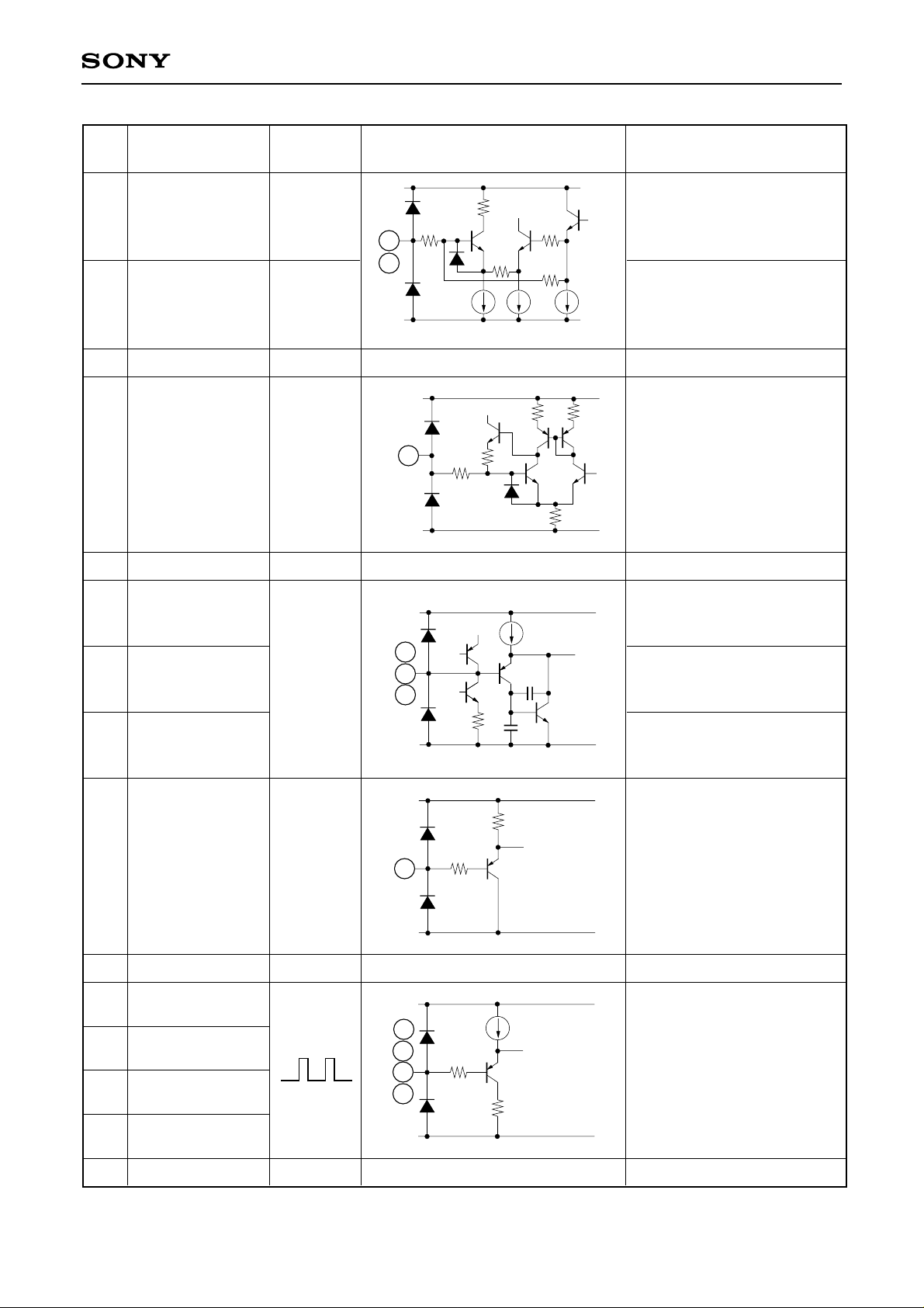
Pin Description (VCC1 = 5V, VCC2 = 13V)
Pin
NO.
Symbol Pin voltage Equivalent circuit Description
1 RGB MBRT
4 R MBRT
5 B MBRT
7 GAM OUT
1.6 to 5.0V
1.6 to 5.0V
1.6 to 5.0V
2V
Reference level
VCC1
2k
40µA
80k
80k
80k
80k
RGB signal common main
brightness control. Preset
internally to 3.3V.
40µA
R signal main brightness
control. Preset internally to
3.3V.
200
1
∗
40µA
GND
VCC1
∗
200
4
5
37k
5k
74k
B signal main brightness
∗
GND
20µA
20µA
VCC1
100
40µA
control. Preset internally to
3.3V.
G signal output of which main
bright and gamma are
7
adjusted and insert the
reference signal.
GND
100
8VCC1 5V 5V power supply.
9 RIN
10 GIN
11 BIN
12 GND GND.
SID OUT SID signal output.
13
0V
9.3Vp-p
Typ.
VCC1
10
11
GND
VCC2
GND
50µA
9
200
6.2k
10
10
13
R signal input.
Input a 0.7Vp-p signal.
G signal input.
Input a 0.7Vp-p signal.
B signal input.
Input a 0.7Vp-p signal.
Note 1)∗ in the Pin voltage indicates external applied voltage.
Note 2) Defined as the amplitude from the pedestal level to white.
Note 2)
Note 2)
Note 2)
– 3 –
Page 4

CXA1853AQ
Pin
NO.
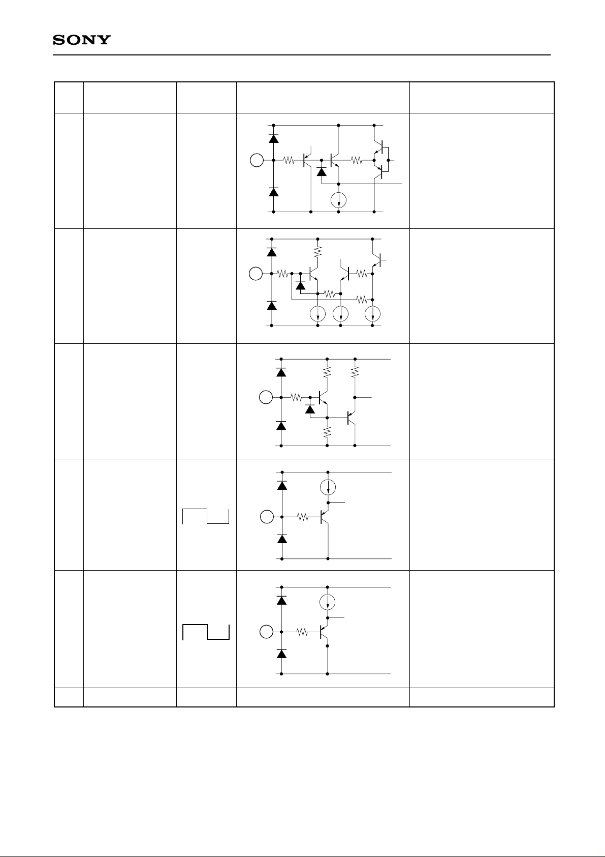
14 VCC2 13V
15 R OUT R signal output.
16 G OUT G signal output.
17 B OUT B signal output.
18 VCC3 5V power supply.
22 GND GND.
23 RGB SBRT
Symbol Pin voltage Equivalent circuit Description
13V power supply.
VCC2
4.5V
Typ.
10
10
GND
15
16
17
5V
0V
VCC3
3k
1.6 to 5.0V
200
23
∗
53µA 13µA
GND
27k
200
RGB signal common sub
brightness control.
53µA
VCC3
24 B SBRT
25 R SBRT
26 B CLP
27 G CLP
28 R CLP
1.6 to 5.0V
1.6 to 5.0V
4.7 to 8.3V
∗
24
25
∗
GND
VCC2
26
∗
27
28
GND
3k
200
26µA 40µA
200
Note)∗in the Pin voltage indicates external applied voltage.
118k
26µA
80k
80k
2k
10µA
B signal sub brightness
control.
Preset internally to 3.3V.
R signal sub brightness
control.
Preset internally to 3.3V.
B output detection signal
input.
G output detection signal
input.
R output detection signal
input.
– 4 –
Page 5
CXA1853AQ
Pin
NO.
Symbol Pin voltage Equivalent circuit Description
29 SID CLP
30 SID CTR
31 PRG CTR
4.7 to 8.3V
1.6 to 5.0V
1.6 to 5.0V
VCC2
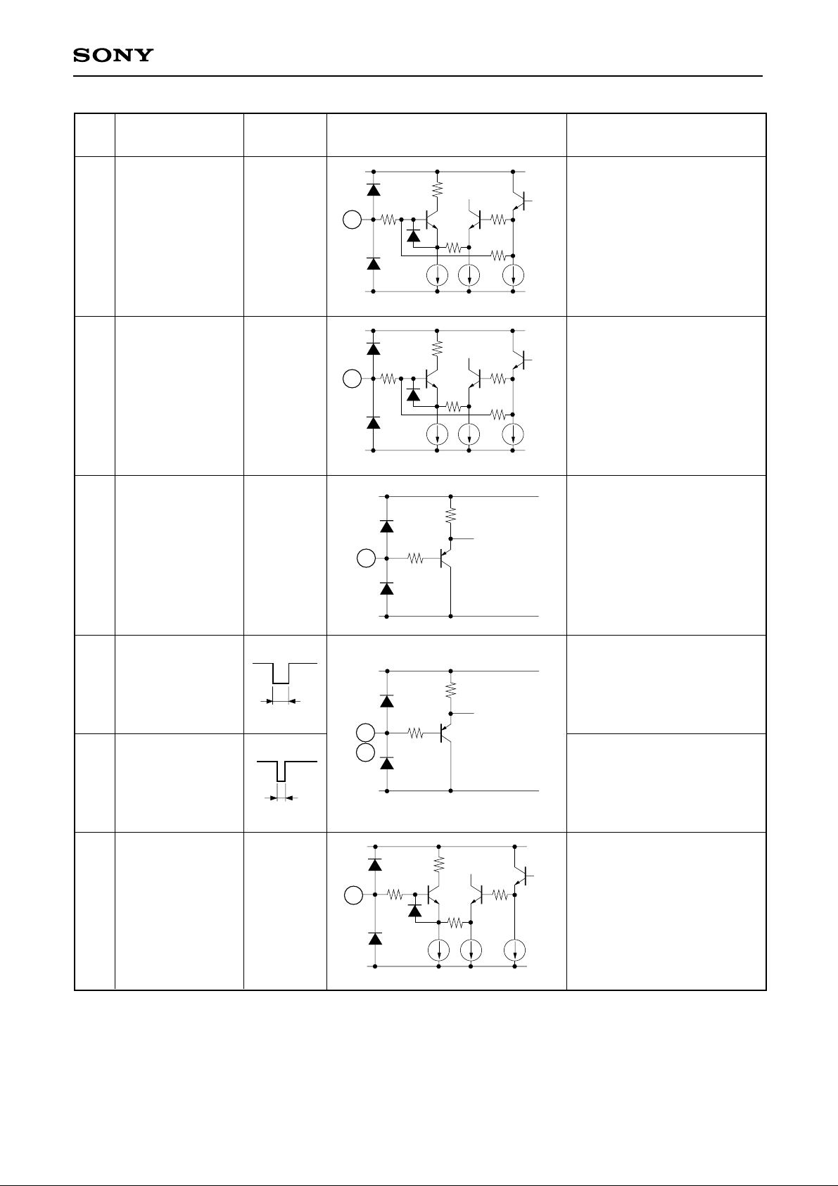
SID output detection signal
200
29
∗
2k
input.
Use an average value
detecting external capacitor
with a small leak current
10µA
GND
VCC3
3k
200
30
∗
53µA 40µA
GND
VCC3
200
∗
31
35k
3k
80k
80k
53µA
90k
absolute value and
tolerance.
SID output amplitude control.
Preset internally to 3.3V.
Level control for the PRG
signal inserted into the SID
signal.
90k
GND
VCC3
10µA
32 FRP
33
SID FRP
34 GND GND.
0V
0V
5V
32
GND
VCC3
5V
33
GND
0V
200
10µA
200
Note)∗in the Pin voltage indicates external applied voltage.
FRP input. This pulse is
used to invert the polarity of
the RGB output. Output is
inverted when Low, and noninverted when High.
Input level: High ≥ 4V
Low ≤ 1V
FRP pulse input for SID
output. This pulse is used to
invert the polarity of the SID
output. Output is inverted
when Low, and non-inverted
when High.
Input level: High ≥ 4V
Low ≤ 1V
– 5 –
Page 6

CXA1853AQ
Pin
NO.
Symbol Pin voltage Equivalent circuit Description
35 PRG
36 VCOM CTR
37 SIG CENT CTR
5V
0V
1.6 to 5.0V
1.6 to 5.0V
VCC3
10µA
PRG pulse input.
This pulse is used to insert
35
200
the PRG signal into the SID
output.
Input level: High ≥ 4V
Low ≤ 1V
GND
VCC2
200
36
∗
17µA
GND
VCC2
200
37
∗
50k
50k
80k
80k
40µA
17µA
80k
80k
VCOM voltage control. The
VCOM voltage variable
range is –0.8V to +1.3V with
respect to the signal center
voltage.
RGB and SID signal center
voltage control.
26µA 40µA
GND
VCC2
38 VCOM OUT VCOM voltage output.
39 BLK LIM
3.4 to 9.1V
1.6 to 5.0V
∗
GND
VCC2
200
39
∗
2k
10
10
127k
26µA
100k
100k
38
Limiter control for limiting the
output amplitude of the RGB
signal. Preset internally to
3.3V.
20µA 40µA
GND
20µA
Note)∗in the Pin voltage indicates external applied voltage.
– 6 –
Page 7
CXA1853AQ
Pin
NO.
Symbol Pin voltage Equivalent circuit Description
40 BLK CENT
41 WHT LIM
42 GAM SEL
1.6 to 5.0V
1.6 to 5.0V
∗
5.0V
VCC2
2k
200
40
∗
50k
100k
100k
RGB signal output limiter
center control. Preset
internally to 3.3V.
When preset, the limiter
center becomes equal to the
20µA 40µA
GND
VCC3
200
41
∗
20µA 40µA
GND
VCC1
200
42
2k
55k
37k
20µA
100k
100k
20µA
RGB output center.
RGB signal white peak
limiter control. Preset
internally to 3.3V.
Gamma circuit control.
Gamma ON when High,
gamma OFF when Low.
Input level: High ≥ 4V
Low ≤ 1V
GND
5V
43 XCLP2
44 XCLP1
45
RGB GAIN
0V
2.0µs
5V
0V
1.2µs
1.6 to 5.0V
VCC1
55k
200
43
44
GND
VCC4
1.5k
200
45
∗
40µA 20µA
GND
Note)∗in the Pin voltage indicates external applied voltage.
38k
40µA
200
Reference signal pulse input.
Reference level when Low.
Input level: High ≥ 4V
Low ≤ 1V
Clamp pulse input. Clamped
when Low.
Input level: High ≥ 4V
Low ≤ 1V
Gain control for RGB signal
common variable gain
amplifier.
– 7 –
Page 8
CXA1853AQ
Pin
NO.
46 R GAIN
Symbol Pin voltage Equivalent circuit Description
1.6 to 5.0V
VCC4
200
1k
48k
80k
80k
∗
46
47
Gain control for R signal
variable gain amplifier.
Preset internally to 3.3V.
Gain control for B signal
47 B GAIN
1.6 to 5.0V
48 GND GND.
49 IREF
50 VCC4 5V power supply.
1.2V
5.0V
∗
GND
0V
VCC4
80µA 40µA
80µA
49
GND
2k
200
variable gain amplifier.
Preset internally to 3.3V.
5k 5k
Sample-and -hold circuit
current setting.
10k
51 GCADET B
52 GCADET G
53 GCADET R
54 SIG SEL
55 GND
56 SH4
57 SH3
58 SH2
61 SH1
1.8V Typ.
0 to 5.0V
0V
5V
0V
VCC4
40µA
51
52
53
6.2k
GND
VCC4
55k
∗
54
200
B GCA circuit clamp
detection.
G GCA circuit clamp
detection.
R GCA circuit clamp
detection.
Selection of input signal to
Sample-and -hold circuit.
R and B signals selected
when High, G signal selected
when Low.
Input level: High ≥ 4V
GND
Low ≤ 1V
GND.
PVCC
56
57
58
59
GND
100µA
200
100
Sample-and-hold pulse
input.
Input level: High ≥ 3.0V
Low ≤ 1.0V
Sampling when High, hold
when Low.
62 PVCC
5V
Note)∗in the Pin voltage indicates external applied voltage.
– 8 –
5V power supply.
Page 9
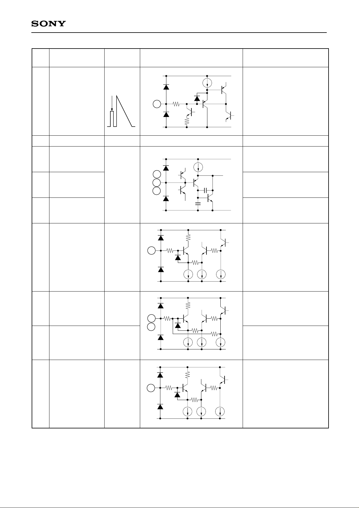
CXA1853AQ
Pin
NO.
63 SH IN
64 GND GND.
65 B CLAMP B signal clamp detection.
66 G CLAMP G signal clamp detection.
67 R CLAMP R signal clamp detection.
Symbol Pin voltage Equivalent circuit Description
2.25V
Reference level
VCC4
63
GND
200
6.2k
100µA
Sample-and-hold circuit
input.
0V
VCC1
40µA
65
2.1V Typ.
66
67
GND
68
69
70
71
RGB GAM
GAIN 1
R GAM
GAIN 1
B GAM
GAIN 1
RGB GAM
GAIN 2
1.6 to 5.0V
1.6 to 5.0V
1.6 to 5.0V
1.6 to 5.0V
VCC1
1k
200
68
∗
40µA
GND
VCC1
∗
200
69
70
37k
1k
37k
40µA
200
80k
80k
RGB signal common black
side voltage gain control.
40µA
R signal black side voltage
gain control. Preset internally
to 3.3V.
B signal black side voltage
∗
GND
VCC1
71
∗
40µA 40µA
40µA
1k
200
37k
200
gain control. Preset internally
to 3.3V.
RGB signal common white
side voltage gain control.
40µA
GND
Note)∗in the Pin voltage indicates external applied voltage.
– 9 –
40µA
40µA
Page 10
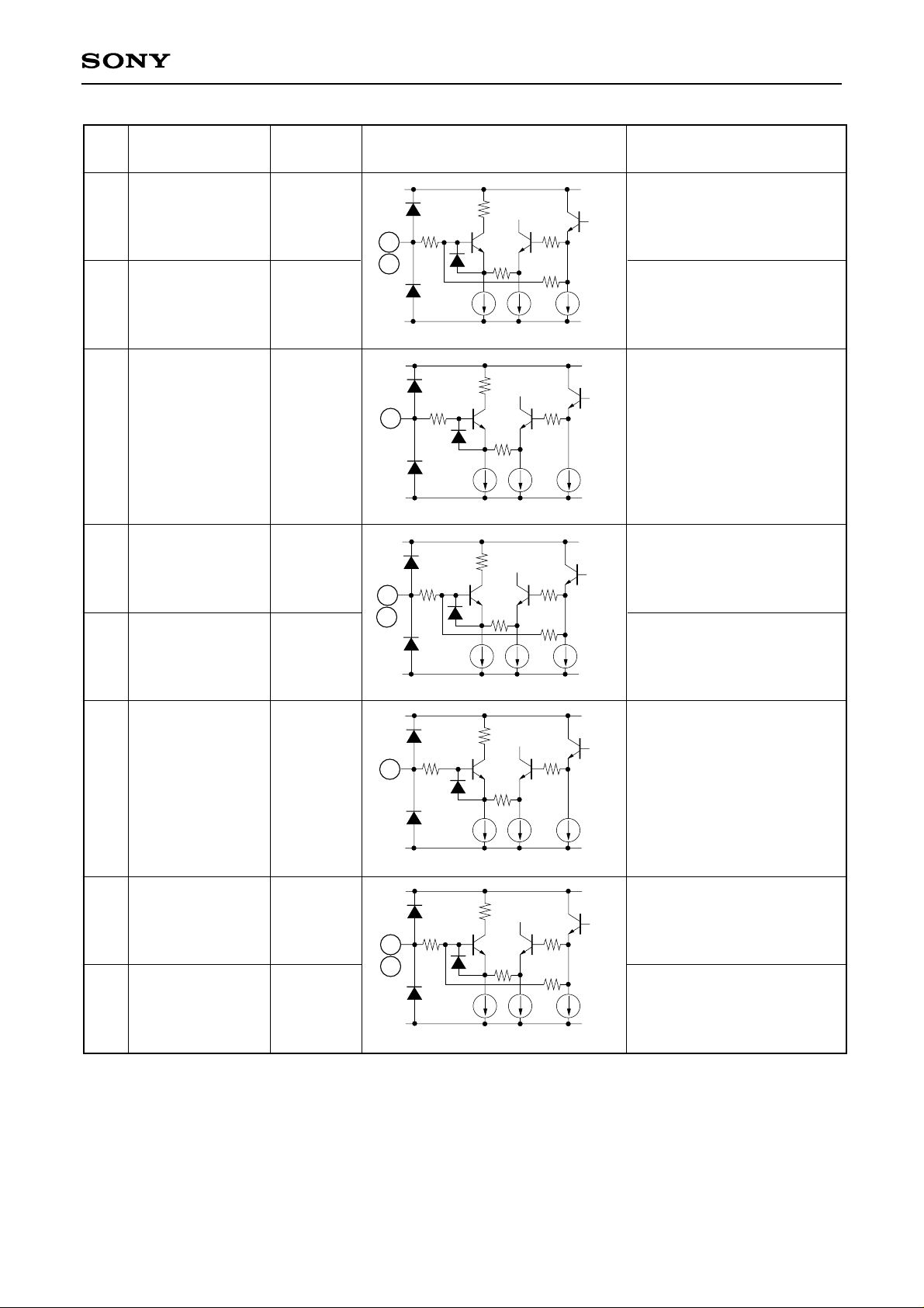
CXA1853AQ
Pin
NO.
72
73
74
75
76
Symbol Pin voltage Equivalent circuit Description
R GAM
GAIN 2
B GAM
GAIN 2
RGB GAM
CTR 2
R GAM
CTR 2
B GAM
CTR 2
1.6 to 5.0V
1.6 to 5.0V
1.6 to 5.0V
1.6 to 5.0V
1.6 to 5.0V
VCC1
∗
72
73
∗
GND
VCC1
74
∗
GND
VCC1
∗
75
76
∗
GND
1k
200
37k
40µA 40µA
1k
200
37k
40µA 40µA
3k
200
74k
20µA 40µA
80k
80k
40µA
200
40µA
80k
80k
20µA
R signal white side voltage
gain control. Preset internally
to 3.3V.
B signal white side voltage
gain control. Preset internally
to 3.3V.
RGB signal common white
side voltage gain change
point control.
R signal white side voltage
gain change point control.
Preset internally to 3.3V.
B signal white side voltage
gain change point control.
Preset internally to 3.3V.
VCC1
1k
200
77
∗
40µA 40µA
GND
VCC1
∗
78
79
∗
GND
3k
200
20µA 40µA
77
78
79
RGB GAM
CTR 1
R GAM
CTR 1
B GAM
CTR 1
1.6 to 5.0V
1.6 to 5.0V
1.6 to 5.0V
Note)∗in the Pin voltage indicates external applied voltage.
37k
74k
40µA
20µA
200
80k
80k
RGB signal common black
side voltage gain change
point control.
R signal black side voltage
gain change point control.
Preset internally to 3.3V.
B signal black side voltage
gain change point control.
Preset internally to 3.3V.
– 10 –
Page 11
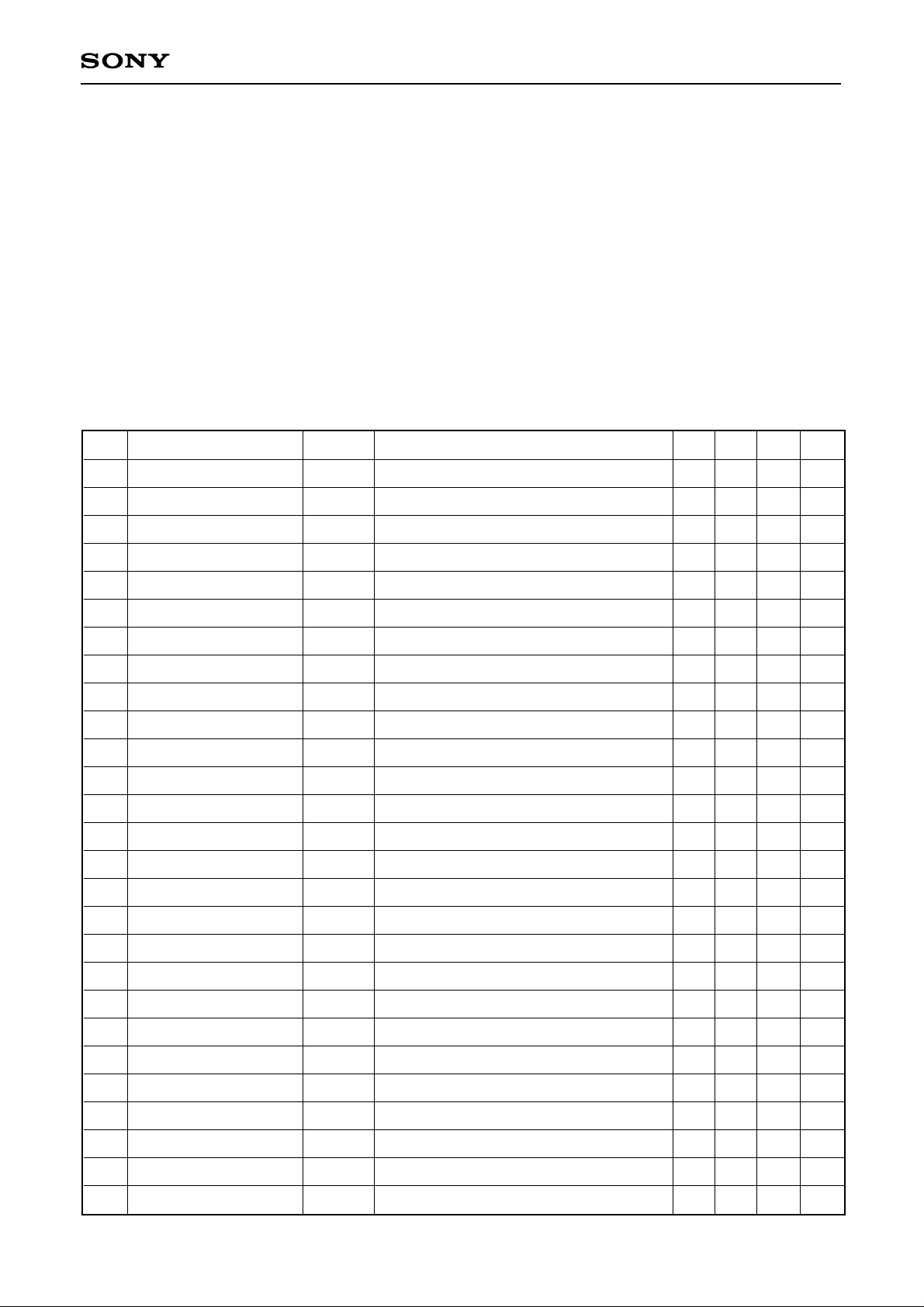
Electrical Characteristics
Unless otherwise specified: Ta = 25°C, VCC1 = VCC3 = VCC4 = PVCC = 5V, VCC2 = 13V
SW1 = OFF, SW4 = OFF, SW5 = OFF, SW9 = a, SW10 = a, SW11 = a,
SW24 = OFF, SW25 = OFF, SW26 = a, SW27 = a, SW28 = a, SW29 = a,
SW30 = OFF, SW36 = OFF, SW37 = OFF, SW39 = OFF, SW40 = OFF,
SW41 = OFF, SW46 = OFF, SW47 = OFF, SW51 = a, SW52 = a,
SW53 = a, SW63 = a, SW65 = a, SW66 = a, SW67 = a, SW69 = OFF,
SW70 = OFF, SW72 = OFF, SW73 = OFF, SW75 = OFF, SW76 = OFF,
SW78 = OFF, SW79 = OFF, V23 = 3.1V, V31 = 3.5V, V42 = 5.0V,
V45 = 2.8V, V54 = 5.0V, V68 = 1.6V, V71 = 1.6V, V74 = 1.6V, V77 = 5.0V
Set (R IN), (G IN), (B IN) and (TEST IN) = 0V, (SH1), (SH2), (SH3) and
(SH4) = 5V, and input SG4 to (FRP) and (SID FRP), SG5 to (PRG),
SG2 to (XCLP2) and SG3 to (XCLP1).
CXA1853AQ
No. Item Symbol Measurement conditions Unit
1
Current consumption (1)
2
Current consumption (2)
3
Current consumption (3)
4
Current consumption (4)
5
Current consumption (5)
6
R IN pin current “Z”
7
R IN pin current “H”
8
R IN pin current “L”
9
G IN pin current “Z”
10
G IN pin current “H”
11
G IN pin current “L”
12
B IN pin current “Z”
13
B IN pin current “H”
14
B IN pin current “L”
15
RGB SBRT pin current
16
B CLP pin current
I
CC1
ICC2
ICC3
ICC4
ICC5
IZ9
IH9
IL9
IZ10
IH10
IL10
IZ11
IH11
IL11
I23
I26
Measure the current entering Pin 8.
Measure the current entering Pin 14.
Measure the current entering Pin 18.
Measure the current entering Pin 50.
Measure the current entering Pin 62.
SW9 → b, (XCLP1) = 5V, V9 = 2.4V
SW9 → b, (XCLP1) = 0V, V9 = 3.4V
SW9 → b, (XCLP1) = 0V, V9 = 1.4V
SW10 → b, (XCLP1) = 5V, V10 = 2.4V
SW10 → b, (XCLP1) = 0V, V10 = 3.4V
SW10 → b, (XCLP1) = 0V, V10 = 1.4V
SW11 → b, (XCLP1) = 5V, V11 = 2.4V
SW11 → b, (XCLP1) = 0V, V11 = 3.4V
SW11 → b, (XCLP1) = 0V, V11 = 1.4V
V23 = 5.0V
SW26 → b, V26 = 7.0V
Min. Typ. Max.
—
30
44
—
11
18
—
6
10
—
29
43
—
4
7
–1.5
–1.5
–1.5
–0.2
13
—
13
—
13
—
—
0
25
–25
0
25
–25
0
25
–25
2.5
0
1.5
—
–13
1.5
—
–13
1.5
—
–13
6
0.2
mA
mA
mA
mA
mA
µA
µA
µA
µA
µA
µA
µA
µA
µA
µA
µA
17
G CLP pin current
18
R CLP pin current
19
SID CLP pin current
20
PRG CTR pin current
21
FRP pin current “H”
22
FRP pin current “L”
23
SID FRP pin current “H”
24
SID FRP pin current “L”
25
PRG pin current “H”
26
PRG pin current “L”
27
GAM SEL pin current “H”
I27
I28
I29
I31
IH32
IL32
IH33
IL33
IH35
IL35
IH42
SW27 → b, V27 = 7.0V
SW28 → b, V28 = 7.0V
SW29 → b, V29 = 7.0V
V31 = 5.0V
(FRP) = 5V
(FRP) = 0V
(SID FRP) = 5V
(SID FRP) = 0V
(PRG) = 5V
(PRG) = 0V
V42 = 5V
– 11 –
–0.2
–0.2
–0.2
—
–0.1
–0.3
–0.1
–0.3
–0.1
–0.3
–0.1
0
0
0
0.3
0
–0.1
0
–0.1
0
–0.1
0
0.2
0.2
0.2
0.8
0.1
—
0.1
—
0.1
—
0.1
µA
µA
µA
µA
µA
µA
µA
µA
µA
µA
µA
Page 12
CXA1853AQ
No. Item Symbol Measurement conditions Min. Typ. Max. Unit
28
GAM SEL pin current “L”
29
XCLP2 pin current “H”
30
XCLP2 pin current “L”
31
XCLP1 pin current “H”
32
XCLP1 pin current “L”
33
RGB GAIN pin current
34
GCA DET B pin current “Z”
35
GCA DET B pin current “H”
36
GCA DET B pin current “L”
37
GCA DET G pin current “Z”
38
GCA DET G pin current “H”
39
GCA DET G pin current “L”
40
GCA DET R pin current “Z”
IL42
IH43
IL43
IH44
IL44
I45
IZ51
IH51
IL51
IZ52
IH52
IL52
IZ53
V42 = 0V
(XCLP2) = 5V
(XCLP2) = 0V
(XCLP1) = 5V
(XCLP1) = 0V
V45 = 5V
SW51 → b, (XCLP1) = 5V, V51 = 2.0V
SW51 → b, (XCLP1) = 0V, V51 = 3.0V
SW51 → b, (XCLP1) = 0V, V51 = 1.0V
SW52 → b, (XCLP1) = 5V, V52 = 2.0V
SW52 → b, (XCLP1) = 5V, V52 = 3.0V
SW52 → b, (XCLP1) = 5V, V52 = 1.0V
SW53 → b, (XCLP1) = 5V, V53 = 2.0V
—
–0.1
—
–0.1
–1.0
—
–0.5
15
—
–0.5
15
—
–0.5
–1.7
0
–1.0
0
–0.2
0.5
0
30
30
0
30
–30
0
–0.4
0.1
–0.3
0.1
—
1.3
0.5
—
–15
0.5
—
–15
0.5
µA
µA
µA
µA
µA
µA
µA
µA
µA
µA
µA
µA
µA
41
GCA DET R pin current “H”
42
GCA DET R pin current “L”
43
SIG SEL pin current “H”
44
SIG SEL pin current “L”
45
SH4 pin current “H”
46
SH4 pin current “L”
47
SH3 pin current “H”
48
SH3 pin current “L”
49
SH2 pin current “H”
50
SH2 pin current “L”
51
SH1 pin current “H”
52
SH1 pin current “L”
53
SH IN pin current “Z”
54
SH IN pin current “H”
55
SH IN pin current “L”
56
B CLAMP pin current “Z”
57
B CLAMP pin current “H”
IH53
IL53
I54H
I54L
I56H
I56L
I57H
I57L
I58H
I58L
I61H
I61L
IZ63
IH63
IL63
IZ65
IH65
SW53 → b, (XCLP1) = 5V, V53 = 3.0V
SW53 → b, (XCLP1) = 5V, V53 = 1.0V
V54 = 5V
V54 = 0V
(SH4) = 5V
(SH4) = 0V
(SH3) = 5V
(SH3) = 0V
(SH2) = 5V
(SH2) = 0V
(SH1) = 5V
(SH1) = 0V
SW63 → b, (XCLP1) = 5V, V63 = 2.2V
SW63 → b, (XCLP1) = 0V, V63 = 3.2V
SW63 → b, (XCLP1) = 0V, V63 = 1.2V
SW65 → b, (XCLP1) = 5V, V65 = 2.0V
SW65 → b, (XCLP1) = 0V, V65 = 3.0V
15
—
–0.1
–3.0
–0.1
–5.0
–0.1
–5.0
–0.1
–5.0
–0.1
–5.0
–1.5
13
—
–0.5
15
30
–30
0
–1.0
0
–2.0
0
–2.0
0
–2.0
0
–2.0
0
25
–25
0
40
—
–15
0.1
—
0.1
—
0.1
—
0.1
—
0.1
—
1.5
—
–13
0.5
—
µA
µA
µA
µA
µA
µA
µA
µA
µA
µA
µA
µA
µA
µA
µA
µA
µA
58
B CLAMP pin current “L”
59
G CLAMP pin current “Z”
60
G CLAMP pin current “H”
61
G CLAMP pin current “L”
62
R CLAMP pin current “Z”
63
R CLAMP pin current “H”
64
R CLAMP pin current “L”
65
RGB GAM GAIN1 pin current
IL65
IZ66
IH66
IL66
IZ67
IH67
IL67
I68
SW65 → b, (XCLP1) = 0V, V65 = 1.0V
SW66 → b, (XCLP1) = 5V, V66 = 2.0V
SW66 → b, (XCLP1) = 0V, V66 = 3.0V
SW66 → b, (XCLP1) = 0V, V66 = 1.0V
SW67 → b, (XCLP1) = 5V, V67 = 2.0V
SW67 → b, (XCLP1) = 0V, V67 = 3.0V
SW67 → b, (XCLP1) = 0V, V67 = 1.0V
V68 = 5.0V
– 12 –
—
–0.5
15
—
–0.5
15
—
—
–40
0
40
–40
0
40
–40
0.5
–15
0.5
—
–15
0.5
—
–15
1.3
µA
µA
µA
µA
µA
µA
µA
µA
Page 13
CXA1853AQ
No. Item Symbol Measurement conditions Min. Typ. Max. Unit
66
RGB GAM GAIN2 pin current
67
RGB GAM CTR2 pin current
68
RGB GAM CTR1 pin current
69
RIN pin voltage
70
GIN pin voltage
71
BIN pin voltage
72
B SBRT pin voltage
73
R SBRT pin voltage
74
SID CTR pin voltage
75
VCOM CTR pin voltage
76
SIG CENT CTR pin voltage
77
BLK LIM pin voltage
78
BLK CENT pin voltage
I71
I74
I77
V9
V10
V11
V24
V25
V30
V36
V37
V39
V40
V71 = 5.0V
V74 = 5.0V
V77 = 5.0V
—
—
—
1.3
1.3
1.3
2.9
2.9
2.9
2.9
2.9
2.9
2.9
0.5
0.5
0.5
1.7
1.7
1.7
3.3
3.3
3.3
3.3
3.3
3.3
3.3
1.3
1.3
1.3
2.1
2.1
2.1
3.7
3.7
3.7
3.7
3.7
3.7
3.7
µA
µA
µA
V
V
V
V
V
V
V
V
V
V
79
WHT LIM pin voltage
80
R GAIN pin voltage
81
B GAIN pin voltage
82
IREF pin voltage
83
GCA DET B pin voltage
84
GCA DET G pin voltage
85
GCA DET R pin voltage
86
SH IN pin voltage
87
B CLAMP pin voltage
88
G CLAMP pin voltage
89
R CLAMP pin voltage
90
R GAM GAIN1 pin voltage
91
B GAM GAIN1 pin voltage
92
R GAM GAIN2 pin voltage
93
B GAM GAIN2 pin voltage
94
R GAM CTR2 pin voltage
95
B GAM CTR2 pin voltage
V41
V46
V47
V49
V51
V52
V53
V63
V65
V66
V67
V69
V70
V72
V73
V75
V76
2.9
2.9
2.9
0.8
1.2
1.2
1.2
1.9
1.6
1.6
1.6
2.9
2.9
2.9
2.9
2.9
2.9
3.3
3.3
3.3
1.2
1.8
1.8
1.8
2.3
2.1
2.1
2.1
3.3
3.3
3.3
3.3
3.3
3.3
3.7
3.7
3.7
1.6
2.4
2.4
2.4
2.7
2.6
2.6
2.6
3.7
3.7
3.7
3.7
3.7
3.7
V
V
V
V
V
V
V
V
V
V
V
V
V
V
V
V
V
96
R GAM CTR1 pin voltage
97
B GAM CTR1 pin voltage
98
RGB MBRT pin voltage
99
R MBRT pin voltage
100
B MBRT pin voltage
RGB MBRT
101
input impedance
V78
V79
V1
V4
V5
Z1
– 13 –
2.9
2.9
2.9
2.9
2.9
45
3.3
3.3
3.3
3.3
3.3
80
3.7
3.7
3.7
3.7
3.7
110
V
V
V
V
V
kΩ
Page 14
CXA1853AQ
No. Item Symbol Measurement conditions Unit
R MBRT
102
input impedance
B MBRT
103
input impedance
B SBRT
104
input impedance
R SBRT
105
input impedance
SID CTR
106
input impedance
VCOM CTR
107
input impedance
SIG CENT CTR
108
input impedance
BLK LIM
109
input impedance
BLK CENT
110
input impedance
WHT LIM
111
input impedance
Z4
Z5
Z24
Z25
Z30
Z36
Z37
Z39
Z40
Z41
Min. Typ. Max.
110
80
45
110
80
45
110
80
45
110
80
45
110
80
45
110
80
45
110
80
45
150
100
55
150
100
55
150
100
55
kΩ
kΩ
kΩ
kΩ
kΩ
kΩ
kΩ
kΩ
kΩ
kΩ
R GAIN
112
input impedance
B GAIN
113
input impedance
R GAM GAIN1
114
input impedance
B GAM GAIN1
115
input impedance
R GAM GAIN2
116
input impedance
B GAM GAIN2
117
input impedance
R GAM CTR2
118
input impedance
B GAM CTR2
119
input impedance
R GAM CTR1
120
input impedance
B GAM CTR1
121
input impedance
Z46
Z47
Z69
Z70
Z72
Z73
Z75
Z76
Z78
Z79
45
45
45
45
45
45
45
45
45
45
80
80
80
80
80
80
80
80
80
80
110
110
110
110
110
110
110
110
110
110
kΩ
kΩ
kΩ
kΩ
kΩ
kΩ
kΩ
kΩ
kΩ
kΩ
– 14 –
Page 15
CXA1853AQ
No. Item Symbol Measurement conditions Unit
Min. Typ. Max.
Set SW41 → ON, V41 = 1.6V, V42 = 0V,
V54 = 0V and input SG1 (0 dB) to (TEST IN).
Then adjust V45 so that the non-inverted
output amplitude (black to white) at TP16 is
5 times the input signal amplitude and label
RGB GAIN
122
adjustment range (1)
∆G
CS1
this as V
Input SG1 (–6 dB) to (TEST IN) and label the
non-inverted output amplitudes (black to white)
at TP15, TP16 and TP17 with V45 = V
V
amplitudes as V
I.
I as
RST, VGST and VBST, and the inverted output
RSTA, VGSTA and VBSTA,
4.0
6.0
—
dB
respectively.
Next, label the non-inverted output amplitudes
(black to white) at TP15, TP16 and TP17 with
V45 = 5.0V as V
inverted output amplitudes as V
RSM, VGSM and VBSM, and the
RSMA, VGSMA
and VBSMA, respectively.
Next, label the non-inverted output amplitudes
(black to white) at TP15, TP16 and TP17 with
RGB GAIN
123
adjustment range (2)
∆GCS2
V45 = 1.6V as V
inverted output amplitudes as V
and VBSNA, respectively.
∆G
CS1 = 20log (VRSM (A)/VRST (A))
= 20log (V
= 20log (V
∆G
CS2 = 20log (VRSN (A)/VRST (A))
= 20log (V
= 20log (V
RSN, VGSN and VBSN, and the
RSNA, VGSNA
GSM (A)/VGST (A))
BSM (A)/VBST (A))
GSN (A)/VGST (A))
BSN (A)/VBST (A))
—
–6.0
–4.0
dB
R GAIN
124
adjustment range (1)
R GAIN
125
adjustment range (2)
B GAIN
126
adjustment range (1)
B GAIN
127
adjustment range (2)
∆GRS1
∆GRS2
∆GBS1
∆GBS2
Set V42 = 0V, V54 = 0V, input SG1 (–6dB)
to (TEST IN), and set V45 = V
I, SW46 → ON,
SW41 → ON, V41 = 1.6V and V46 = 5.0V.
Then label the non-inverted output amplitude
(black to white) at TP15 as V
inverted output amplitude as V
RSTM and the
RSTMA.
Next, label the non-inverted output amplitude
(black to white) at TP15 with V46 = 1.6V as
V
RSTN and the inverted output amplitude as
V
RSTNA.
∆G
RS1 = 20log (VRSTM (A)/VGST (A))
∆G
RS2 = 20log (VRSTN (A)/VGST (A))
Set V42 = 0V, V54 = 0V, input SG1 (–6dB)
to (TEST IN), and set V45 = V
I, SW47 → ON,
SW41 → ON, V41 = 1.6V and V47 = 5.0V.
Then label the non-inverted output amplitude
(black to white) at TP17 as V
inverted output amplitude as V
BSTM and the
BSTMA.
Next, label the non-inverted output amplitude
(black to white) at TP17 with V47 = 1.6V as
V
BSTN and the inverted output amplitude as
V
BSTNA.
∆G
BS1 = 20log (VBSTM (A)/VGST (A))
∆G
BS2 = 20log (VBSTN (A)/VGST (A))
2.5
—
2.5
—
4.6
–4.6
4.6
–4.6
—
–2.5
—
–2.5
dB
dB
dB
dB
– 15 –
Page 16
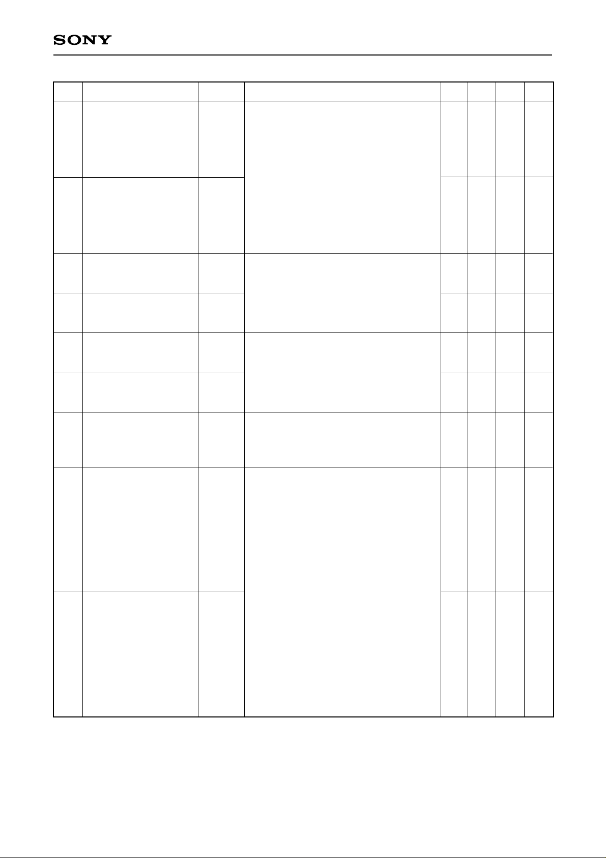
CXA1853AQ
No. Item Symbol Measurement conditions Unit
Min. Typ. Max.
Label the DC potentials at TP9, TP10 and
RGB MBRT
128
adjustment range (1)
∆V
BM1
TP11 as V
Next, label the DC potentials at TP9, TP10
and TP11 with SW1 → ON and V1 = 5.0V
RT, VGT and VBT, respectively.
—
–0.35
–0.30
V
as VRN, VGN and VBN, respectively.
Next, label the DC potentials at TP9, TP10
RGB MBRT
129
adjustment range (2)
∆VBM2
and TP11 with V1 = 1.6 V as V
V
BM, respectively.
∆V
BM1 = VRN – VRT, VGN – VGT,
V
BN – VBT
RM, VGM and
0.30
0.35
—
V
∆VBM2 = VRM – VRT, VGM – VGT,
V
BM – VBT
R MBRT
130
adjustment range (1)
∆VBR1
Label the DC potential at TP9 with SW4 → ON
and V4 = 5.0V as V
RTN.
—
–0.16
–0.12
V
Next, label the DC potential at TP9 with V4 =
R MBRT
131
adjustment range (2)
B MBRT
132
adjustment range (1)
∆VBR2
∆VBB1
1.6V as V
∆V
∆VBR2 = VRTM – VGT
Label the DC potential at TP11 with SW5 → ON
and V5 = 5.0V as V
RTM.
BR1 = VRTN – VGT
BTN.
0.12
—
0.16
–0.16
—
–0.12
V
V
Next, label the DC potential at TP11 with V5 =
B MBRT
133
adjustment range (2)
∆VBB2
1.6V as V
∆V
∆VBB2 = VBTM – VGT
BTM.
BB1 = VBTN – VGT
0.12
0.16
—
V
Maximum RGB output
134
amplitude
RGB SBRT
135
adjustment range (1)
RGB SBRT
136
adjustment range (2)
∆VBMAX
VSBN
VSBM
Set SW39 → ON, V39 = 1.6V, V45 = 5.0V and
V23 = 5.0V.
Then measure the amplitudes (black to black)
at TP15, TP16 and TP17.
Set SW39 → ON and V39 = 1.6V.
Then label the non-inverted reference level
potentials at TP15, TP16 and TP17 as V
V
SGT and VSBT, and the inverted reference
level potentials as V
SRTA, VSGTA and VSBTA,
SRT,
respectively.
Next, label the non-inverted reference level
potentials at TP15, TP16 and TP17 with V23 =
1.6V as V
inverted reference level potentials as V
V
SGNA and VSBNA, respectively.
SRN, VSGN and VSBN, and the
SRNA,
Next, label the non-inverted reference level
potentials at TP15, TP16 and TP17 with
V23 = 5.0V as V
SRM, VSGM and VSBM, and
the inverted reference level potentials as
V
SRMA, VSGMA and VSBMA, respectively.
V
SBN =VSRNA – VSRN, VSGNA – VSGN,
V
SBNA – VSBN
VSBM =VSRMA – VSRM, VSGMA – VSGM,
V
SBMA – VSBM
10.0
—
8.5
10.7
–0.7
10.7
—
—
Vp-p
V
0
V
– 16 –
Page 17
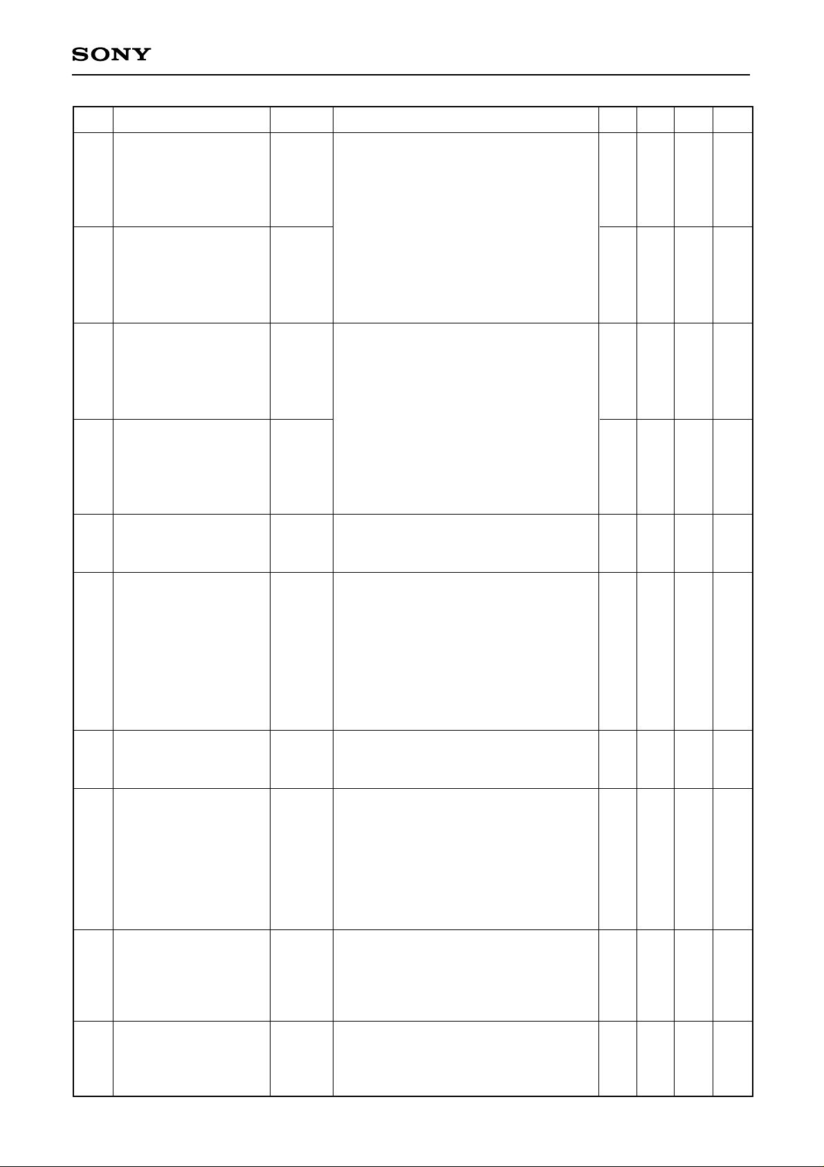
CXA1853AQ
No. Item Symbol Measurement conditions Unit
Min. Typ. Max.
Set SW39→ ON, V39 = 1.6V, SW25→ ON and
R SBRT
137
adjustment range (1)
∆V
SSR1
V25 = 1.6V. Then label the non-inverted reference
level potential at TP15 as V
reference level potential as V
SRTN and the inverted
SRTNA.
—
–1.8
–1.2
V
Next, label the non-inverted reference level potential
R SBRT
138
adjustment range (2)
∆VSSR2
at TP15 with V25 = 5.0V as V
reference level potential as V
∆
VSSR1 = (VSRTNA – VSRTN)
– (V
SGTA – VSGT)
∆
VSSR2 = (VSRTMA – VSRTM)
– (V
SGTA – VSGT)
SRTM and the inverted
SRTMA.
1.2
1.8
—
V
Set SW39→ ON, V39 = 1.6V, SW24→ ON and
B SBRT
139
adjustment range (1)
∆VSSB1
V24 = 1.6V. Then label the non-inverted reference
level potential at TP17 as V
reference level potential as V
SBTN and the inverted
SBTNA.
—
–1.8
–1.2
V
Next, label the non-inverted reference level potential
B SBRT
140
adjustment range (2)
∆VSSB2
at TP17 with V24 = 5.0V as V
reference level potential as V
∆
VSSB1 = (VSBTNA – VSBTN)
– (V
SGTA – VSGT)
∆
VSSB2 = (VSBTMA – VSBTM)
– (V
SGTA – VSGT)
SBTM and the inverted
SBTMA.
1.2
1.8
—
V
Reference level difference
141
between R, G and B
Gain difference between
142
R, G and B
Difference between the
inverted and non-inverted
143
gain
Difference between the
144
reference level and 50 IRE
∆VS
∆GRGB
∆GINV
∆V50I
∆
VS = VSRT (A) – VSGT (A),
V
SGT (A) – VSBT (A),
V
SBT (A) – VSRT (A)
Set V45 = VI, SW41→ ON, V41 = 1.6V and input
SG1 (0dB) to (R IN), (G IN) and (B IN).
Then label the non-inverted output amplitudes (black
to white) at TP15, TP16 and TP17 as V
RVT, VGVT
and VBVT, and the inverted output amplitudes as
V
RVTA, VGVTA and VBVTA, respectively.
∆
GRGB = 20log (VBVT/VRVT),
20log (V
RVT/VGVT),
20log (V
GVT/VBVT)
∆
GINV = 20log (VRVT/VRVTA),
20log (V
GVT/VGVTA),
20log (V
BVT/VBVTA)
Set V45 = VI.
Then label the non-inverted output signal reference
level amplitudes at TP15, TP16 and TP17 as V
SR, VSG
and VSB, and the inverted output signal reference level
amplitudes as V
V
50I =VSR (A) – VRVT (A)/2
=V
=V
SRA, VSGA and VSBA, respectively.
SG (A) – VGVT (A)/2
SB (A) – VBVT (A)/2
–200
–0.8
–0.7
–150
0
200
mV
0
0.8
dB
0
0.7
dB
0
150
mV
Gamma intermediate
145
region gain
Minimum RGB gamma
146
black side gain
GGN
GCBN
(See “Black Side Gamma Measurement Method”.)
Set V45 = V
I.
Then measure the minimum gain GN of the noninverted and inverted signals at TP15, TP16 and TP17.
G
GN = 20 log (GN)
(See “Black Side Gamma Measurement Method”.)
Set V45 = VI, V23 = 1.6V and V77 = 1.6V.
Then obtain the gamma gain of the non-inverted and
inverted signals at TP15, TP16 and TP17.
– 17 –
8.0
–1.5
9.8
0
12.0
1.5
dB
dB
Page 18
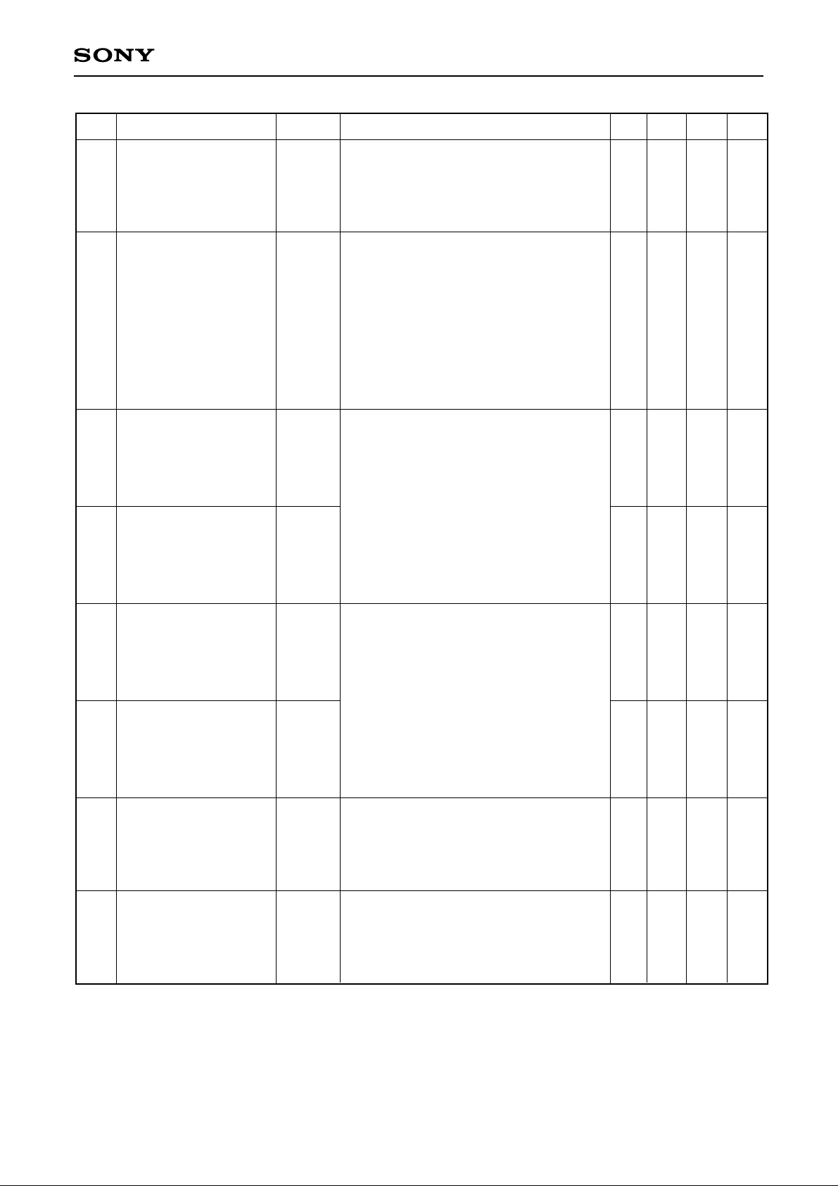
CXA1853AQ
No. Item Symbol Measurement conditions Unit
Min. Typ. Max.
(See “Black Side Gamma Measurement Method”.)
Maximum RGB gamma
147
black side gain
∆G
GBM
Set V45 = V
1.6V.
Then obtain the gamma gain of the non-inverted
I, V23 = 1.6V, V68 = 5.0V and V77 =
15
18
—
dB
and inverted signals at TP15, TP16 and TP17.
(See “Black Side Gamma Measurement Method”.)
Set V45 = V
I, V23 = 1.6V, V68 = 3.0V and V77 =
1.6V.
Gamma black side gain
difference between R, G
148
and B
∆GGBT
Then label the non-inverted side gamma gain at
TP15, TP16 and TP17 as G
and the inverted side gamma gain as G
G
BGTA and GBBTA, respectively.
∆
GGBT =GBRT (A) – GBGT (A)
BRT, GBGT and GBBT,
BRTA,
–1.0
0
1.0
dB
=GBGT (A) – GBBT (A)
=GBBT (A) – GBRT (A)
(See “Black Side Gamma Measurement Method”.)
R gamma black side sub
149
gain adjustment range (1)
R gamma black side sub
150
gain adjustment range (2)
∆GGBR1
∆GGBR2
Set V45 = V
SW69
Then measure the gamma gain at TP15, and label
the non-inverted side as G
side as G
∆
GGBR1 = GBRN (A) – GBGT (A)
Next, measure the gamma gain at TP15 with
V69 = 5.0V, and label the non-inverted side as
G
BRM and the inverted side as GBRMA.
∆
GGBR2 = GBRM (A) – GBGT (A)
I, V23 = 1.6V, V68 = 3.0V, V77 = 1.6V,
→
ON and V69 = 1.6V.
BRN and the inverted
BRNA
—
2.5
–4.5
4.5
–2.5
—
dB
dB
B gamma black side sub
151
gain adjustment range (1)
B gamma black side sub
152
gain adjustment range (2)
Minimum RGB gamma
153
white side gain
Maximum RGB gamma
154
white side gain
∆GGBB1
∆GGBB2
GGWN
GGWN
(See “Black Side Gamma Measurement Method”.)
Set V45 = V
SW70
I, V23 = 1.6V, V68 = 3.0V, V77 = 1.6V,
→
ON and V70 = 1.6V.
Then measure the gamma gain at TP17, and label
the non-inverted side as G
side as G
∆
GGBB1 = GBBN (A) – GBGT (A)
BBNA.
BBN and the inverted
Next, measure the gamma gain at TP17 with
V70 = 5.0V, and label the non-inverted side as
G
BBM and the inverted side as GBBMA.
∆
GGBB2 = GBBM (A) – GBGT (A)
(See “White Side Gamma Measurement Method”.)
Set V45 = V
I, V23 = 1.6V, SW41
→
ON, V41 =
1.6V, V71 = 1.6V and V74 = 5.0V.
Then measure the gamma gain of the non-inverted
and inverted sides at TP15, TP16 and TP17.
(See “White Side Gamma Measurement Method”.)
Set V45 = V
I, V23 = 1.6V, SW41
→
ON, V41 =
1.6V, V71 = 5.0V and V74 = 5.0V.
Then measure the gamma gain of the non-inverted
and inverted sides at TP15, TP16 and TP17.
—
2.5
–1.5
15
–4.5
4.5
0
18
–2.5
—
1.5
—
dB
dB
dB
dB
– 18 –
Page 19

CXA1853AQ
No. Item Symbol Measurement conditions Unit
Min. Typ. Max.
(See “White Side Gamma Measurement Method”.)
Set V45 = V
5.0V, SW41
I, V23 = 1.6V, V71 = 3.0V, V74 =
→
ON and V41 = 1.6V.
Then label the non-inverted side gamma gain
Gamma white side gain
155
difference between R, G
and B
∆G
GWT
at TP15, TP16 and TP17 as G
G
WBT, and the inverted side gamma gain as
G
WRTA, GWGTA and GWBTA, respectively.
∆
GGWT = GWRT (A) – GWGT (A)
WRT, GWGT and
–1.0
0
1.0
dB
= GWGT (A) – GWBT (A)
= GWBT (A) – GWRT (A)
(See “White Side Gamma Measurement Method”.)
R gamma white side sub
156
gain adjustment range (1)
∆GGWR1
Set V45 = V
5.0V, SW41
and V72 = 1.6V.
I, V23 = 1.6V, V71 = 3.0V, V74 =
→
ON, V41 = 1.6V, SW72→ ON
—
–4.5
–2.5
dB
Then measure the gamma gain at TP15, and
R gamma white side sub
157
gain adjustment range (2)
∆GGWR2
label the non-inverted side as G
inverted side as G
∆
GGWR1 = GWRN (A) – GWGT (A)
WRNA.
Next, measure the gamma gain at TP15 with
V72 = 5.0V, and label the non-inverted side as
G
WRM and the inverted side as GWRMA.
∆
GGWR2 = GWRM (A) – GWGT (A)
WRN and the
2.5
4.5
—
dB
B gamma white side sub
158
gain adjustment range (1)
B gamma white side sub
159
gain adjustment range (2)
Minimum RGB gamma
160
black side breakpoint value
Maximum RGB gamma
161
black side breakpoint value
∆GGWB1
∆GGWB2
PGBN
PGBM
(See “White Side Gamma Measurement Method”.)
Set V45 = V
5.0V, SW41
I, V23 = 1.6V, V71 = 3.0V, V74 =
→
ON, V41 = 1.6V, SW73→ ON
and V73 = 1.6V.
Then measure the gamma gain at TP17, and
label the non-inverted side as G
inverted side as G
∆
GGWB1 = GWBN (A) – GWGT (A)
WBNA.
WBN and the
Next, measure the gamma gain at TP17 with
V73 = 5.0V, and label the non-inverted side as
G
WBM and the inverted side as GWBMA.
∆
GGWB2 = GWBM (A) – GWGT (A)
(See “Black Side Gamma Measurement Method”.)
Set V45 = V
I, V23 = 1.6V, V68 = 5.0V and V77 =
1.6V.
Then measure the gamma breakpoints of the
non-inverted and inverted sides at TP15, TP16
and TP17.
(See “Black Side Gamma Measurement Method”.)
Set V45 = V
5.0V, SW1
I, V23 = 1.6V, V68 = 5.0V, V77 =
→
ON and V1 = 4.0V.
Then measure the gamma breakpoints of the
non-inverted and inverted sides at TP15, TP16
and TP17.
—
2.5
–0.45
—
–4.5
4.5
–0.15
–1.05
–2.5
—
—
–0.75
dB
dB
V
V
– 19 –
Page 20

CXA1853AQ
No. Item Symbol Measurement conditions Unit
Min. Typ. Max.
(See “Black Side Gamma Measurement Method”.)
Set V45 = V
I, V23 = 1.6V, V68 = 5.0V and V77 = 3.3V.
Then measure the gamma breakpoints at TP15,
Gamma black side
162
breakpoint difference
between R, G and B
∆P
GBT
TP16 and TP17 and label the non-inverted side
as P
GBRT, PGBGT and PGBBT, and the inverted
side as P
∆
GBRTA, PGBGTA and PGBBTA, respectively.
PGBT = PGBRT (A) – PGBGT (A)
–0.15
0
0.15
V
= PGBGT (A) – PGBBT (A)
= PGBBT (A) – PGBRT (A)
(See “Black Side Gamma Measurement Method”.)
R gamma black side
163
breakpoint sub adjustment
range (1)
R gamma black side
breakpoint sub adjustment
164
range (2)
∆PGBR1
∆PGBR2
Set V45 = V
SW78
Then measure the gamma breakpoint at TP15, and
label the non-inverted side as P
inverted side as P
∆
PGBR1 = PGBRN (A) – PGBGT (A)
Next, measure the gamma breakpoint at TP15 with
V78 = 5.0V, SW1
the non-inverted side as P
side as P
∆
PGBR2 = PGBRM (A) – PGBGT (A)
I, V23 = 1.6V, V68 = 5.0V, V77 = 3.3V,
→
ON and V78 = 1.6V.
GBRN and the
GBRNA.
→
ON and V1 = 4.0V, and label
GBRM and the inverted
GBMA.
0.15
—
0.3
–0.3
—
–0.15
V
V
(See “Black Side Gamma Measurement Method”.)
B gamma black side
breakpoint sub adjustment
165
range (1)
B gamma black side
breakpoint sub adjustment
166
range (2)
∆PGBB1
∆PGBB2
Set V45 = V
SW79
Then measure the gamma breakpoint at TP17, and
label the non-inverted side as P
inverted side as P
∆
PGBB1 = PGBBN (A) – PGBGT (A)
Next, measure the gamma breakpoint at TP17 with
V79 = 5.0V, SW1
the non-inverted side as P
as P
∆
PGBB2 = PGBBM (A) – PGBGT (A)
I, V23 = 1.6V, V68 = 5.0V, V77 = 3.3V,
→
ON and V79 = 1.6V.
GBBN and the
GBBNA.
→
ON and V1 = 4.0V, and label
GBBM and the inverted side
GBBMA.
0.15
—
0.3
–0.3
—
–0.15
V
V
Minimum RGB gamma
167
white side breakpoint value
Maximum RGB gamma
168
white side breakpoint value
Gamma white side
breakpoint difference
169
between R, G and B
PGWN
PGWM
∆PGWT
(See “White Side Gamma Measurement Method”.)
Set V45 = V
SW41
I, V23 = 1.6V, V71 = 5.0V, V74 = 5.0V,
→
ON and V41 = 1.6V.
Then measure the gamma breakpoints of the noninverted and inverted sides at TP15, TP16 and TP17.
(See “White Side Gamma Measurement Method”.)
Set V45 = V
SW1
I, V23 = 1.6V, V71 = 5.0V, V74 = 1.6V,
→
ON, V1 = 2.3V, SW41→ ON and V41 =
1.6V.
Then measure the gamma breakpoints of the noninverted and inverted sides at TP15, TP16 and
TP17.
(See “White Side Gamma Measurement Method”.)
Set V45 = V
SW41
I, V23 = 1.6V, V71 = 5.0V, V74 = 3.3V,
→
ON and V41 = 1.6V.
Then measure the gamma breakpoints at TP15,
TP16 and TP17 and label the non-inverted sides as
P
GWRT, PGWGT and PGWBT, and the inverted sides
as P
GWRTA, PGWGTA and PGWBTA, respectively.
∆
PGWT = PGWRT (A) – PGWGT (A)
= PGWGT (A) – PGWBT (A)
= PGWBT (A) – PGWRT (A)
– 20 –
—
0.75
–0.15
–0.35
1.20
0
–0.05
—
0.15
V
V
V
Page 21
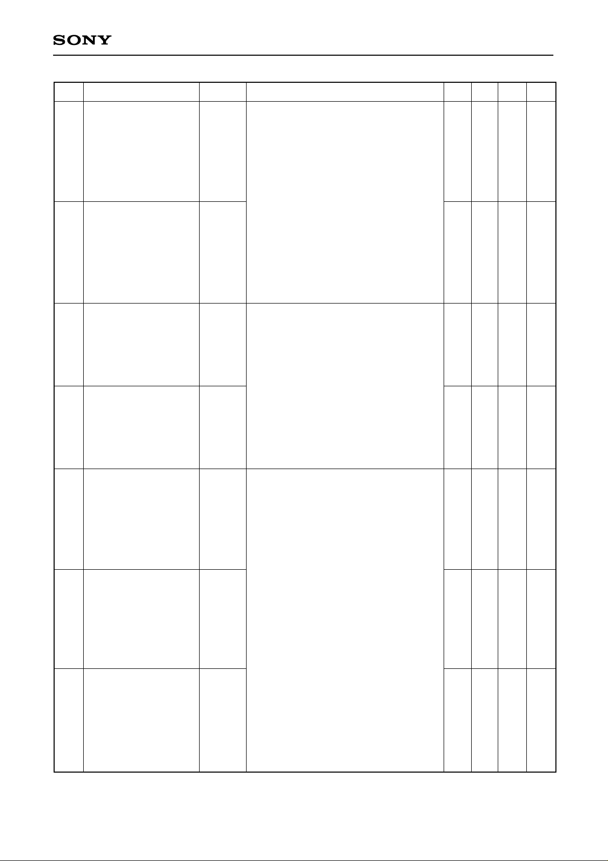
CXA1853AQ
No. Item Symbol Measurement conditions Unit
Min. Typ. Max.
(See “White Side Gamma Measurement Method”.)
R gamma white side
170
breakpoint sub adjustment
range (1)
∆P
GWR1
Set V45 = V
SW41
Then measure the gamma breakpoint at TP16,
and label the non-inverted side as P
inverted side as P
I, V23 = 1.6V, V71 = 5.0V, V74 = 3.3V,
→
ON and V41 = 1.6V.
GWGT and the
GWGTA.
—
–0.3
–0.15
V
Next, measure the gamma breakpoint at TP15 with
SW75
→
ON and V75 = 5.0, and label the non-
R gamma white side
breakpoint sub adjustment
171
range (2)
∆PGWR2
inverted side as P
P
GWRNA.
∆
PGWR1 = PGWRN (A) – PGWGT (A)
Next, measure the gamma breakpoint at TP15 with
V75 = 1.6V, SW1
the non-inverted side as P
side as P
∆
GWRMA.
PGWR2 = PGWRM (A) – PGWGT (A)
GWRN and the inverted side as
→
ON and V1 = 2.3V, and label
GWRM and the inverted
0.15
0.3
—
V
(See “White Side Gamma Measurement Method”.)
B gamma white side
breakpoint sub adjustment
172
range (1)
B gamma white side
breakpoint sub adjustment
173
range (2)
∆PGWB1
∆PGWB2
Set V45 = V
SW41
V76 = 5.0V.
Then measure the gamma breakpoint at TP17,
and label the non-inverted side as P
inverted side as P
∆
PGWB1 = PGWBN (A) – PGWGT (A)
Next, measure the gamma breakpoint at TP17 with
V75 = 1.6V, SW1
the non-inverted side as P
side as P
∆
PGWB2 = PGWBM (A) – PGWGT (A)
I, V23 = 1.6V, V71 = 5.0V, V74 = 3.3V,
→
ON, V41 = 1.6V, SW76→ ON and
GWBN and the
GWBNA.
→
ON and V1 = 2.3V, and set
GWBM and the inverted
GWBMA.
—
0.15
–0.3
0.3
–0.15
—
V
V
WHT LIM standard voltage
174
value
WHT LIM adjustment
175
range (1)
WHT LIM adjustment
176
range (2)
VWT
∆VW1
∆VW2
Set V45 = 5.0V, V42 = 0V, V54 = 0V and input
SG1 (0dB) to (TEST IN).
Label the non-inverted output amplitudes (black to
white) at TP15, TP16 and TP17 as V
WRLT, VWGLT
and VWBLT, and the inverted output amplitudes as
V
WRLTA, VWGLTA and VWBLTA, respectively.
Next, label the non-inverted output amplitudes
(black to white) at TP15, TP16 and TP17 with
SW41
→
ON and V41 = 5.0V as VWRLN, VWGLN
and VWBLN, and the inverted output amplitudes as
V
WRLNA, VWGLNA and VWBLNA, respectively.
Next, label the non-inverted output amplitudes
(black to white) at TP15, TP16 and TP17 with
V41 = 1.6V as V
inverted output amplitudes as V
WRLM, VWGLM and VWBLM, and the
WRLMA, VWGLMA
and VWBLMA, respectively.
V
WT = VWRLT (A), VWGLT (A),
V
WBLT (A)
∆
VW1 = VWRLN (A) – VWRLT (A)
= VWGLN (A) – VWGLT (A)
= VWBLN (A) – VWBLT (A)
∆
VW2 = VWRLM (A) – VWRLT (A)
= VWGLM (A) – VWGLT (A)
VWBLM (A) – VWBLT (A)
1.7
—
2.4
2.0
–1.7
2.8
2.3
–1.3
—
V
V
V
– 21 –
Page 22
CXA1853AQ
No. Item Symbol Measurement conditions UnitMin. Typ. Max.
Set V23 = 1.6V and V37 = 2.8V.
Then label the DC voltages at TP15, TP16 and
BLK LIM standard voltage
177
value (non-inverted side)
TP17 as V
V
BLT
Next, set V23 = 5.0V, SW26 → (b), SW27 → (b),
SW28 → (b), V26 = 7.0V, V27 = 7.0V and V28 =
CR1, VCG1 and VCB1, respectively.
4.2
4.8
5.4
7.0V, and then label the non-inverted limiter levels
at TP15, TP16 and TP17 as V
V
BBLT, and the inverted limiter levels as VBRLTA,
V
BGLTA and VBBLTA, respectively.
BRLT, VBGLT and
Next, label the non-inverted limiter levels at TP15,
TP16 and TP17 with SW39 → ON and V39 =
BLK LIM standard voltage
178
value (inverted side)
VBLTA
1.6V as V
inverted limiter levels as V
V
BBLMA, respectively.
BRLM, VBGLM and VBBLM, and the
BRLMA, VBGLMA and
4.2
4.8
5.4
Next, label the non-inverted limiter levels at TP15,
TP16 and TP17 with V39 = 5.0V as V
BRLN, VBGLN
and VBBLN, and the inverted limiter levels as
V
BRLNA, VBGLNA and VBBLNA, respectively.
V
BLT =VCR1 – VBRLT
BLK LIM adjustment range
179
(1) (non-inverted side)
∆VBL1
=VCG1 – VBGLT
=VCB1 – VBBLT
0.7
1.2
—
VBLTA =VBRLTA – VCR1
=VBGLTA – VCG1
=VBBLTA – VCB1
∆VBL1 = (VCR1 – VBRLM)
– (V
CR1 – VBRLT)
=(V
CG1 – VBGLM)
– (V
BLK LIM adjustment range
180
(2) (non-inverted side)
BLK LIM adjustment range
181
(3) (inverted side)
BLK LIM adjustment range
182
(4) (inverted side)
∆VBL2
∆VBL3
∆VBL4
∆V
BL2 = (VCR1 – VBRLN)
∆V
BL3 = (VBRLMA – VCR1)
∆V
BL4 = (VBRLNA – VCR1)
CG1 – VBGLT)
=(V
CB1 – VBBLM)
– (V
CB1 – VBBLT)
– (V
CR1 – VBRLT)
=(V
CG1 – VBGLN)
– (V
CG1 – VBGLT)
=(V
CB1 – VBBLN)
– (V
CB1 – VBBLT)
– (V
BRLTA – VCR1)
=(V
BGLMA – VCG1)
– (V
BGLTA – VCG1)
=(V
BBLMA – VCB1)
– (V
BBLTA – VCB1)
– (V
BRLTA – VCR1)
=(V
BGLNA – VCG1)
– (V
BGLTA – VCG1)
=(V
BBLNA – VCB1)
– (V
BBLTA – VCB1)
—
–0.5
—
–2.7
0
–2.7
–2.2
0.5
–2.2
V
V
V
V
V
V
RGB output DC voltage
183
SID output DC voltage
184
VCRGB
VCSID
Set V42 = 0V and V23 = 2.1V.
Then label the DC voltages at TP15, TP16 and
TP17 as V
V
CRGB = VCRT, VCGT, VCBT
CRT, VCGT and VCBT, respectively.
Set V31 = 1.6V, SW30 → ON and V30 = 1.6V.
Then measure the DC voltage at TP13.
– 22 –
6.35
6.35
6.50
6.50
6.65
6.65
V
V
Page 23
CXA1853AQ
No. Item Symbol Measurement conditions UnitMin. Typ. Max.
Set V42 = 0V, V31 = 1.6V, SW30 → ON,
V30 = 1.6V and V37 = 2.8V.
Then measure the DC voltages at TP13, TP15,
DC voltage difference
185
between RGB and SID
outputs
∆V
CSRGB
TP16 and TP17, and level these voltages as
V
CS2, VCR2, VCG2 and VCB2, respectively.
∆V
CSRGB = VCS2 – VCR2, VCS2 – VCG2,
V
CS2 – VCB2
–150
0
150
=VCR2 – VCG2, VCR2 – VCB2,
V
CG2 – VCB2
mV
Minimum SIG CENT
186
adjustment voltage
Maximum SIG CENT
187
adjustment voltage
DC voltage difference
between VCOM OUT and
188
RGB output
VCOM control range (1)
189
VCOM control range (2)
190
SID OUT amplitude
191
Maximum SID CTR control
192
voltage
VC1
VC2
∆VCOM
∆VCOM1
∆VCOM2
VSID
VSMAX
Set V42 = 0V, V37 = 5.0V, SW37 → ON.
Then measure the DC voltages at TP13, TP15,
TP16 and TP17.
Set V42 = 0V, V37 = 1.6V, SW37 → ON.
Then measure the DC voltages at TP15, TP16
and TP17.
∆V
COM = VCRT – VCOM
=VCGT – VCOM
=VCBT – VCOM
Set SW36 → ON and V36 = 5.0V.
Then label the voltage at TP38 as V
∆V
COM1 = VCRT – VCOM1
COM1.
=VCGT – VCOM1
=VCBT – VCOM1
Set SW36 → ON and V36 = 1.6V.
Then label the voltage at TP38 as V
∆V
COM2 = VCRT – VCOM2
COM2.
=VCGT – VCOM2
=VCBT – VCOM2
Set V31 = 1.6V.
Then measure the output amplitude at TP13.
Set V31 = 1.6V, SW30 → ON, V30 = 5.0V and
V
CC2 = 13V.
Then measure the output amplitude at TP13.
—
7.7
100
2.1
8.3
10
4.7
8.3
300
–1.9
2.4
9.3
11
5.3
—
500
–1.6
10.3
—
V
V
mV
V
V
Vp-p
Vp-p
Minimum SID CTR control
193
voltage
Maximum PRG CTR
194
control voltage
VSMIN
VPRGM
Set V31 = 1.6V, SW30 → ON, V30 = 1.6V and
V
CC2 = 13V.
Then measure the output amplitude at TP13.
Set V31 = 5.0V.
Then measure the amplitude of the PRG
section using the output waveform at TP13.
VPRG
SG5
– 23 –
—
2.0
5.0
3.2
6.5
—
Vp-p
Vp-p
Page 24
CXA1853AQ
No. Item Symbol Measurement conditions Min. Typ. Max. Unit
Minimum PRG CTR
195
control voltage
Frequency response (1)
196
(RGB input – RGB output)
Frequency response (3)
197
(RGB input – γ)
Slew rate
198
(RGB input – RGB output)
Input dynamic range
199
V
PRGN
fRGB
fγ
SRGB
R
VDIN
Set V31 = 1.6V.
Then measure the amplitude of the PRG
section using the output waveform at TP13.
Frequency response from (R IN), (G IN) and (B
IN) to TP15, TP16 and TP17 (frequency which
goes to –3dB with respect to 100kHz)
Frequency response from (R IN), (G IN) and
(B IN) to the sample-and-hold circuit input
(frequency which goes to –3dB with respect to
100kHz)
Input SG6 to (R IN), (G IN) and (B IN).
Then adjust V45 so that the output amplitude
(black to white) at TP16 is 3V.
Measure the slew rate from the 10 to 90% rise
and fall time of TP15, TP16 and TP17.
Set SW41 → ON, V41 = 1.6V and input SG1
(variable amplitude) to (R IN), (G IN) and (B
IN).
Then label the amplitude of the 1st, 5th and
10th steps as b1, b5 and b10, respectively,
using the non-inverted output waveform at
TP15, TP16 and TP17.
The input dynamic range is defined as the
minimum value for the input amplitude (black
to white) at which b1/b5 < 0.8 or
b10/b5 < 0.8.
—
—
20
60
0.8
0
18
25
100
1.1
0.4
—
—
—
—
Vp-p
MHz
MHz
V/µs
Vp-p
Sample-and-hold circuit
200
droop rate
GAM OUT reference
201
voltage amplitude
GAM OUT GAIN
202
(Maximum GAM gain)
RDLP
VGS
GG
Set V45 = V
and (SH3).
Then measure the droop rate at TP15, TP16
and TP17.
Next, input SG7 to (SH4).
Then measure the droop rate of TP15, TP16
and TP17.
Measure the reference signal voltage amplitude
of TP7.
Input SG1 to (G IN).
Then measure the output amplitude (black to
white) of TP7, and label it as V
I and input SG7 to (SH1), (SH2)
G.
—
0.15
–5.2
—
0.22
–4.2
40
0.29
–3.2
mV/µs
Vp-p
dB
Note) The symbol (A) in the Measurement conditions inscription indicates that the measurement values for
both the inverted and non-inverted sides are used.
(Example)
20 log (VRSM (A)/VRST (A)) means both
20 log (VRSM/VRST) and
20 log (VRSMA/VRSTA).
In this example, VRSM and VRST are non-inverted side measurement values and VRSMA and VRSTA are inverted
side measurement values.
– 24 –
Page 25
CXA1853AQ
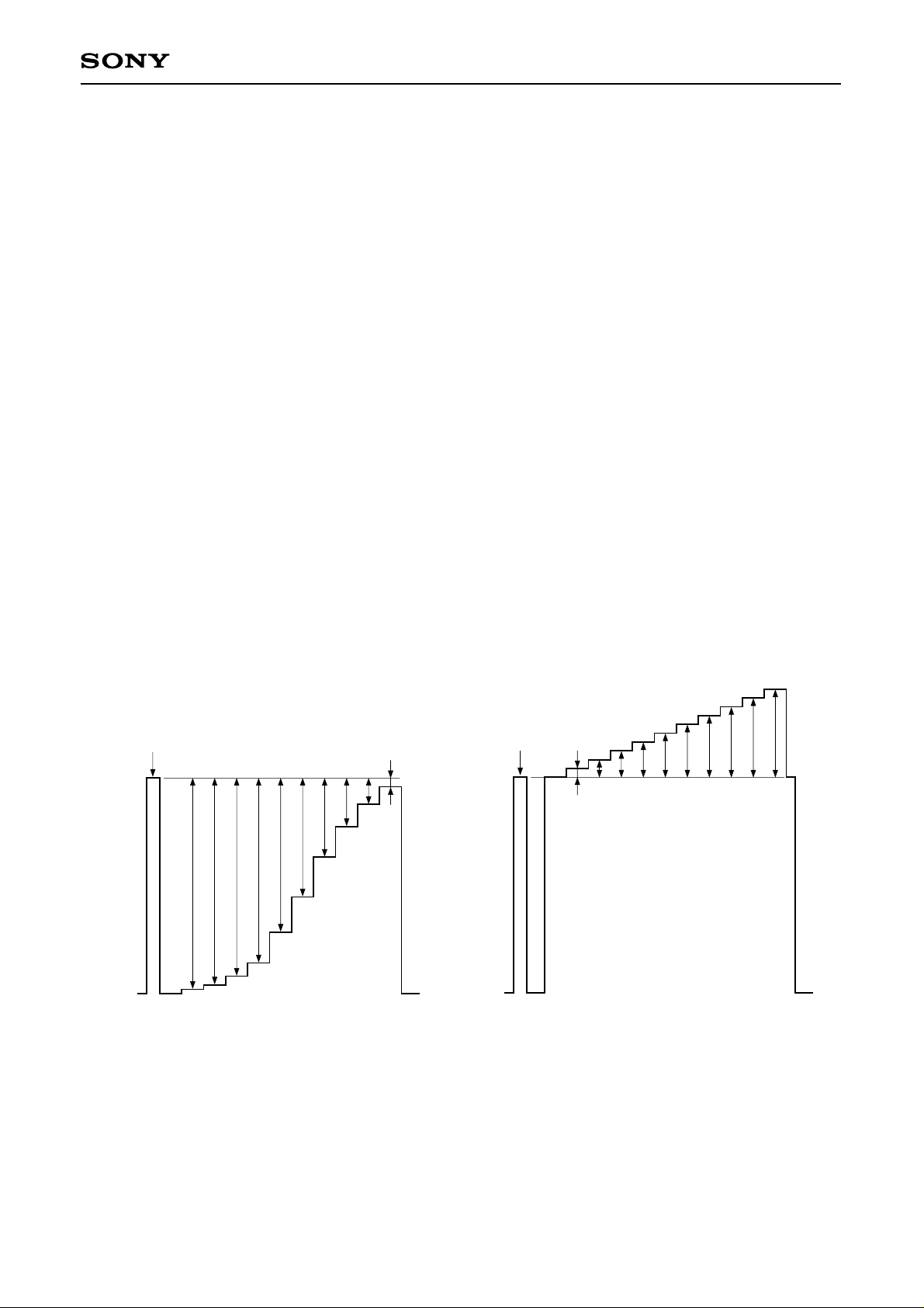
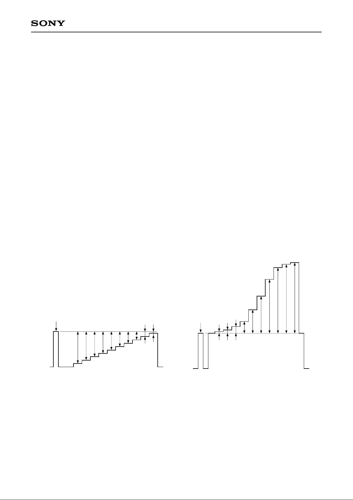
Black Side Gamma Measurement Method
Measure the output voltages y1 to y10 which correspond to the input voltages a1 to a10 using SG8 as the input
signal. (Measure the voltage from the reference level. Label the white side from the reference level as positive,
and the black side as negative.)
Select the two points where | yn – yn–1 | (n = 2 to 10) is a maximum, and label these points yk and yk – 1. Also,
label the input voltages which correspond to yk and yk – 1 as ak and ak – 1, respectively.
Next, measure the output voltages y1 to y10 which correspond to the input voltages a1 to a10 using SG9 as the
input signal.
Select the two points where | yn – yn – 1 | (n = 2 to 10) is a maximum, and label these points yh and yh – 1. Also,
label the input voltages which correspond to yh and yh – 1 as ah and ah – 1, respectively.
From the above:
Maximum gain GM = (yk – yk – 1)/(ak – ak – 1)
Minimum gain GN = (yh – yh – 1)/(ah – ah – 1)
The black side gamma gain is defined as the ratio of the maximum gain to the minimum gain. In other words:
Gamma gain = 20 log (GM/GN)
The gamma breakpoint is defined as the intersection between the straight line passing through points (ak, yk)
and (ak – 1, yk – 1) and the straight line passing through points (ah, yh) and (ah – 1, yh – 1). In other words:
Gamma breakpoint = (GM ∗ GN ∗ (ak – ah) – GN ∗ yk + GM ∗ yh)/(GM – GN)
Reference level
y1
y2
y3
y4
y5
y6
y7
y8
y10
y9
Reference level
y2 y3 y4 y5 y6 y7 y8 y9 y10
y1
RGB output waveform (SG8) RGB output waveform (SG9)
– 25 –
Page 26
CXA1853AQ
White Side Gamma Measurement Method
Measure the output voltages y1 to y10 which correspond to the input voltages a1 to a10 using SG9 as the input
signal. (Measure the voltage from the reference level. Label the white side from the reference level as positive,
and the black side as negative.)
Select the two points where | yn – yn–1 | (n = 2 to 10) is a maximum, and label these points yk and yk – 1. Also,
label the input voltages which correspond to yk and yk – 1 as ak and ak – 1, respectively.
Next, measure the output voltages y1 to y10 which correspond to the input voltages a1 to a10 using SG8 as the
input signal.
Select the two points where | yn – yn – 1 | (n = 2 to 10) is a maximum, and label these points yh and yh – 1. Also,
label the input voltages which correspond to yh and yh – 1 as ah and ah – 1, respectively.
From the above:
Maximum gain GM = (yk – yk – 1)/(ak – ak – 1)
Minimum gain GN = (yh – yh – 1)/(ah – ah – 1)
The white side gamma gain is defined as the ratio of the maximum gain to the minimum gain. In other words:
Gamma gain = 20 log (GM/GN)
The gamma breakpoint is defined as the intersection between the straight line passing through points (ak, yk)
and (ak – 1, yk – 1) and the straight line passing through points (ah, yh) and (ah – 1, yh – 1). In other words:
Gamma breakpoint = (GM ∗ GN ∗ (ak – ah) – GN ∗ yk + GM ∗ yh)/(GM – GN)
Reference level
y9 y10
y8y7y6y5y4y3y2y1
Reference level
y1
y4 y5 y6 y7 y8 y9 y10
y2 y3
RGB output waveform (SG8)
RGB output waveform (SG9)
– 26 –
Page 27
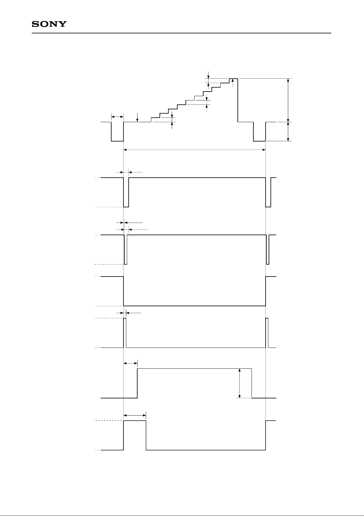
Input Waveforms
CXA1853AQ
SG1
SG2
5V
0V
5V
10-step linear waveform
0dB
Black
5µs
Amplitude of the 1st step
2µs
0.4µs
1.2µs
Amplitude of the 10th step
White
0.714V
Amplitude of the 5th step
0.286V
64µs
SG3
SG4
SG5
SG6
0V
5V
0V
5V
0V
5V
1µs
6µs
0.714V
tr, tf < 5ns
10µs
SG7
0V
– 27 –
Page 28
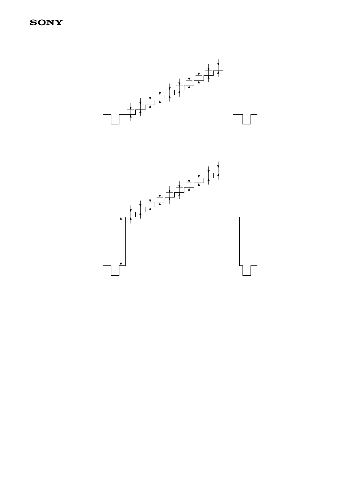
SG8 35mV
35mV
35mV
35mV
CXA1853AQ
35mV
35mV
35mV
35mV
35mV
35mV
35mV
35mV
35mV
35mV
35mV
35mV
35mV
35mV
35mV
35mV
SG9
350mV
– 28 –
Page 29
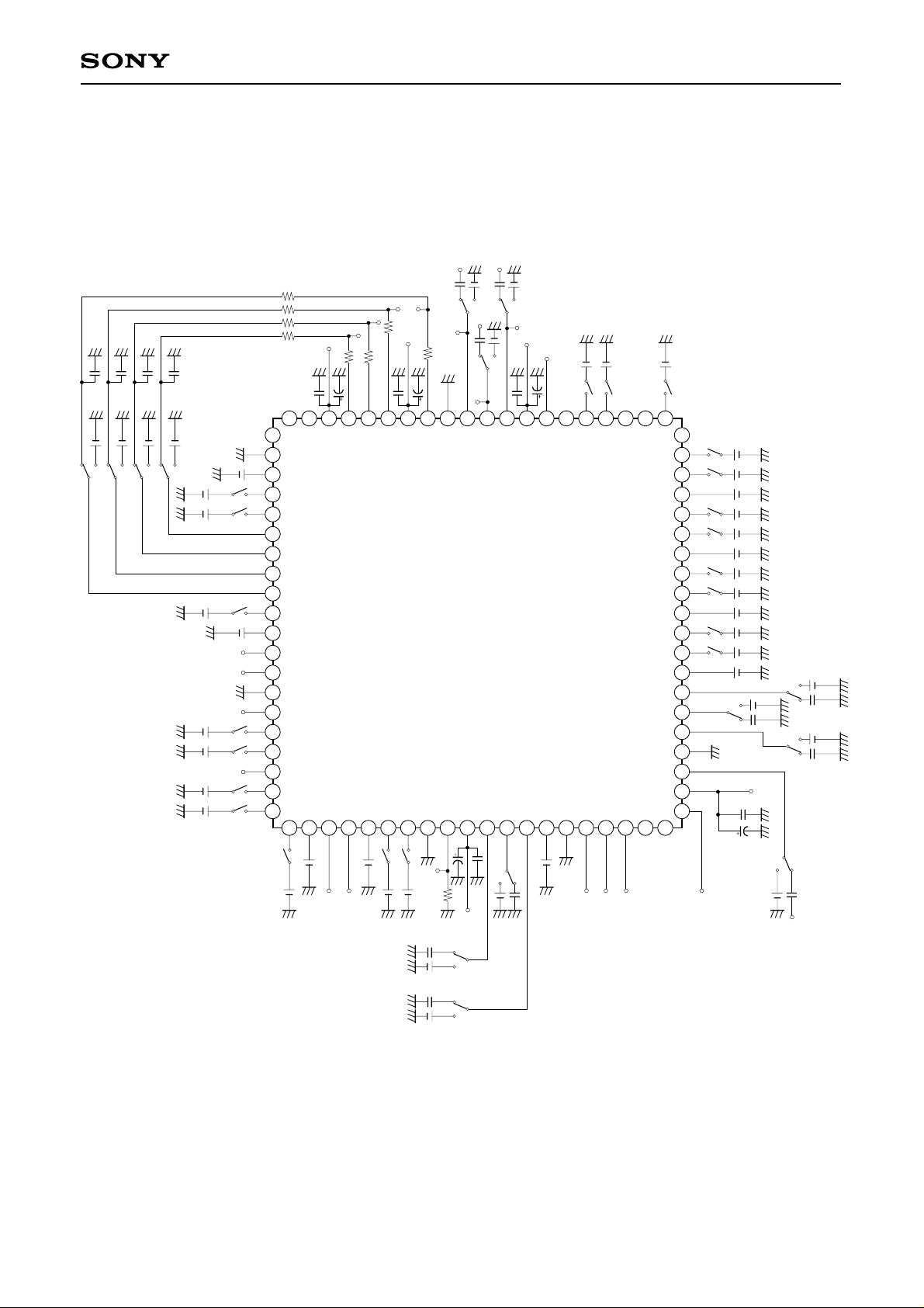
Electrical Characteristics Measurement Circuit
TP17
100µ
100
17
44
(XCLP1)
V45
TP16
16
45
100
V46
TP15
15
46
SW46
100
V47
VCC2
0.1µ
47
(a)
SW29
V29
(a)
(b)
V28
SW28
(b)
(a)
SW27
1µ1µ1µ
V27
(b)
(a)
SW26
1µ
V26
(b)
V24
V25
V30
(SID FRP)
V36
V37
V39
V40
V23
SW24
SW25
SW30
V31
(FRP)
(PRG)
SW36
SW37
TP38
SW39
SW40
390k
390k
390k
390k
21
22
23
24
25
26
27
28
29
30
31
32
33
34
35
36
37
38
39
40
SW41
V41
VCC3
0.1µ
19
18
20
43
41
42
V42
(XCLP2)
TP13
14
SW47
100µ
13
48
TP49
33k
0.1µ
0.1µ
SW11
100
(B IN)
(a)
TP11
12
49
(a)
11
50
100µ
VCC4
(R IN)
(a)
(b)
(G IN)
(a) (b)
TP10
10
51
0.1µ
TP9
SW10
9
52
V52
(b)
SW9
VCC1
0.1µ
53
SW52
(a)(b)
0.1µ
8
TP7
100µ
7
54
V54
V5 V4
SW5
6
5
55
56
(SH4)
4
57
SW4
58
(SH3)
3
(SH2)
CXA1853AQ
V1
SW1
1
2
80
79
SW79
SW78
SW76
SW75
SW73
SW72
SW70
SW69
SW66
(SH1)
V79
V78
V77
V76
V75
V74
V73
V72
V71
V70
V69
V68
(b)
(a)
VCC5
0.1µ
100µ
(b)
SW67
V66
(a)
0.1µ
(b)
SW65
(a)
SW63
(a)
(b)
V63 0.1µ
SH IN
V67
0.1µ
V65
0.1µ
78
77
76
75
74
73
72
71
70
69
68
67
66
65
64
63
62
61
60
59
V51
0.1µ
V53
SW51
(b)
(a)
SW53
(b)
– 29 –
Page 30
CXA1853AQ
Description of Operation
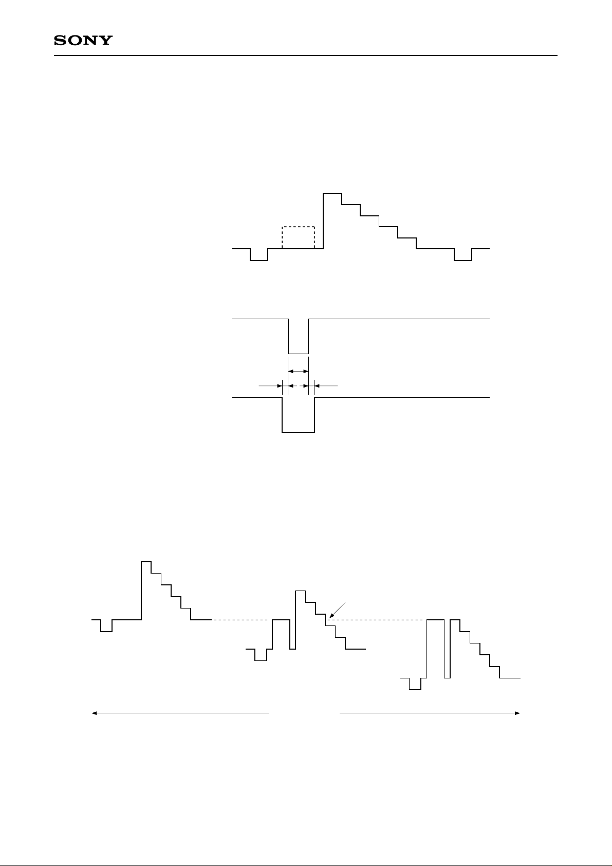
Reference signal
The reference level is inserted into the RGB signal by inputting the XCLP2 signal shown below during the RGB
input signal pedestal level interval. Gamma compensation and clamping operation are performed based on this
level.
Reference
signal
RGB signal input
XCLP1
1.2µ
0.4µ 0.4µ
XCLP2
Bright adjustment
The position of the RGB signal relative to the reference level changes according to the voltage applied to RGB
MBRT (Pin 1). Bright can be controlled without changing the γ characteristics to the panel because the input
bias is changed with the breakpoint for output kept constant.
RGB signal output
50 IRE
Bright pin
Low High
voltage preset
– 30 –
Page 31
CXA1853AQ
Gamma compensation
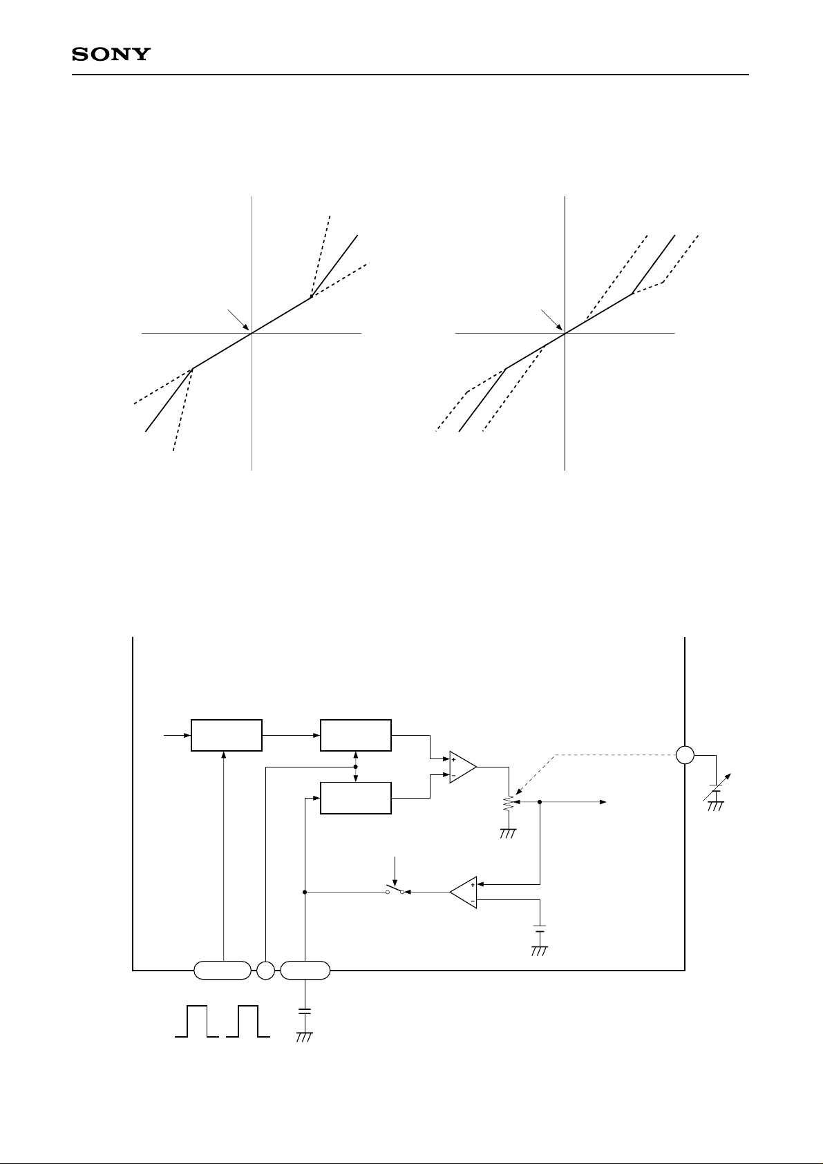
The gamma compensation curve establishes the gain change points (breakpoints) on both the black and white
sides from the reference level. The black and white side gains and the black and white side gain change points
can each be adjusted independently.
Output
Reference level
Reference level
Input
Gain adjustment
Output
Input
Breakpoint variation
Sample-and-hold, gain control and pedestal clamp
Since sample-and-hold circuits are established in the R, G and B lines and each of these circuits is operated
by an independent pulse, the delay can be set freely. In addition, the pulse leak is canceled by establishing a
sample-and-hold circuit in the clamp loop and inputting the differential input of the gain control circuit.
S/H S/H
57, 58, 61
S/H pulse
56
51 to 53
S/H
Clamp pulse
Clamp capacitance
– 31 –
Gain control amplifier
Error amplifier
45
To the
inversion
circuit
Clamp voltage
Page 32
CXA1853AQ
RGB inversion amplifier
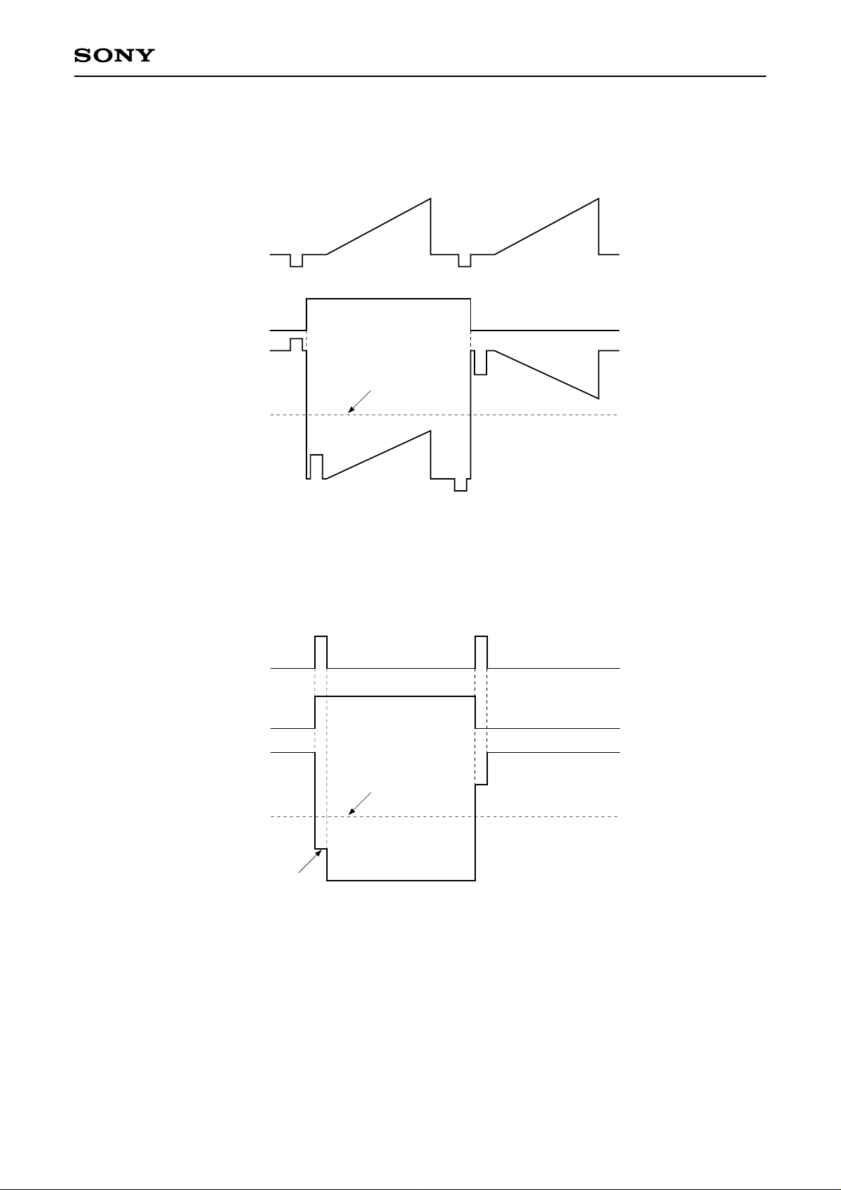
The polarity of the RGB output is inverted according to the FRP pulse. The relationship between input and
output is as shown in the figure below.
RGB IN
FRP
Signal center
RGB OUT
SID output
The CXA1853Q outputs a side black signal for 4:3/16:9 aspect conversion. The black level is adjusted by the
SID CTR pin. In addition, the PRG level can be set in part of the side black signal by inputting the PRG pulse.
The PRG level is adjusted by the PRG CTR pin. The relationship between each input and output is as shown
in the figure below.
PRG
SIDFRP
Signal center
SID OUT
PRG level
Signal center control
The RGB and SID output center voltages are adjusted by the SIG CENT CTR (Pin 37).
When SIG CENT CTR is preset, the output pin center voltage goes to VCC2/2.
Output clamp
The average value of each RGB and SID output signal is detected with external RC circuits and input to the
RGB CLP and SID CLP pins. Then the center voltage offsets among R, G, B and SID outputs are reduced by
feedback which equalizes these detected values and the signal center voltage set by the SIG CENT CTR pin.
– 32 –
Page 33
CXA1853AQ
Notes on Operation
1) R IN (Pin 9), G IN (Pin 10), B IN (Pin 11) input signal impedance
An external capacitor is used as the hold capacitor for the clamp at the input of this IC. Therefore, the input
signal impedance must be sufficiently low (75Ω or less) and the external capacitor must have a small leak
current.
2) Clamp hold capacitors (Pins 51 to 53 and 65 to 67)
The external capacitors connected to these pins must have a small leak current.
3) R, G, B, SID OUT load capacitance
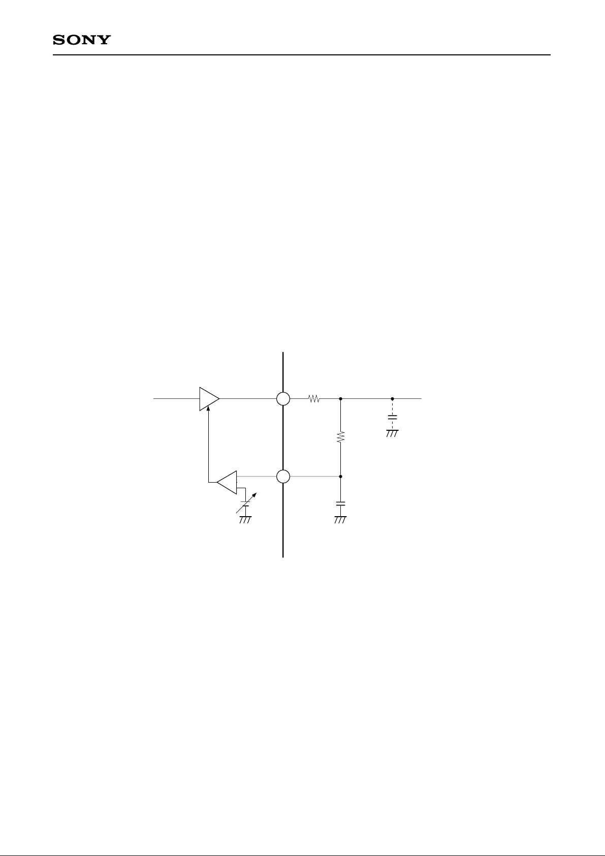
The output signal will tend to oscillate if the R, G, B and SID OUT load capacitance increases. Be sure to
insert a 100 to 220Ω resistor in series to these output pins, and design to keep the load capacitance from
exceeding 30pF.
4) External capacitor at the output
The leak current absolute value and tolerance for the R, G, B and SID OUT average value detecting
capacitors should be small.
Note that if there is an offset in the leak current between R, G and B, offset voltage is also generated
between R, G and B in the external resistor, which causes a DC offset of the output signal.
R, G, B,
SID OUT
R, G, B,
SID CLP
100 to 220Ω
Load capacitance
30pF or less
390kΩ
1µF
5) GND and power supply pins
Pins 12, 22, 34, 48, 55 and 64 (GND) should be set to the minimum identical potential applied to the IC,
and should not be left open. In addition, the potential at Pins 8, 18, 50 and 62 should be the same.
– 33 –
Page 34
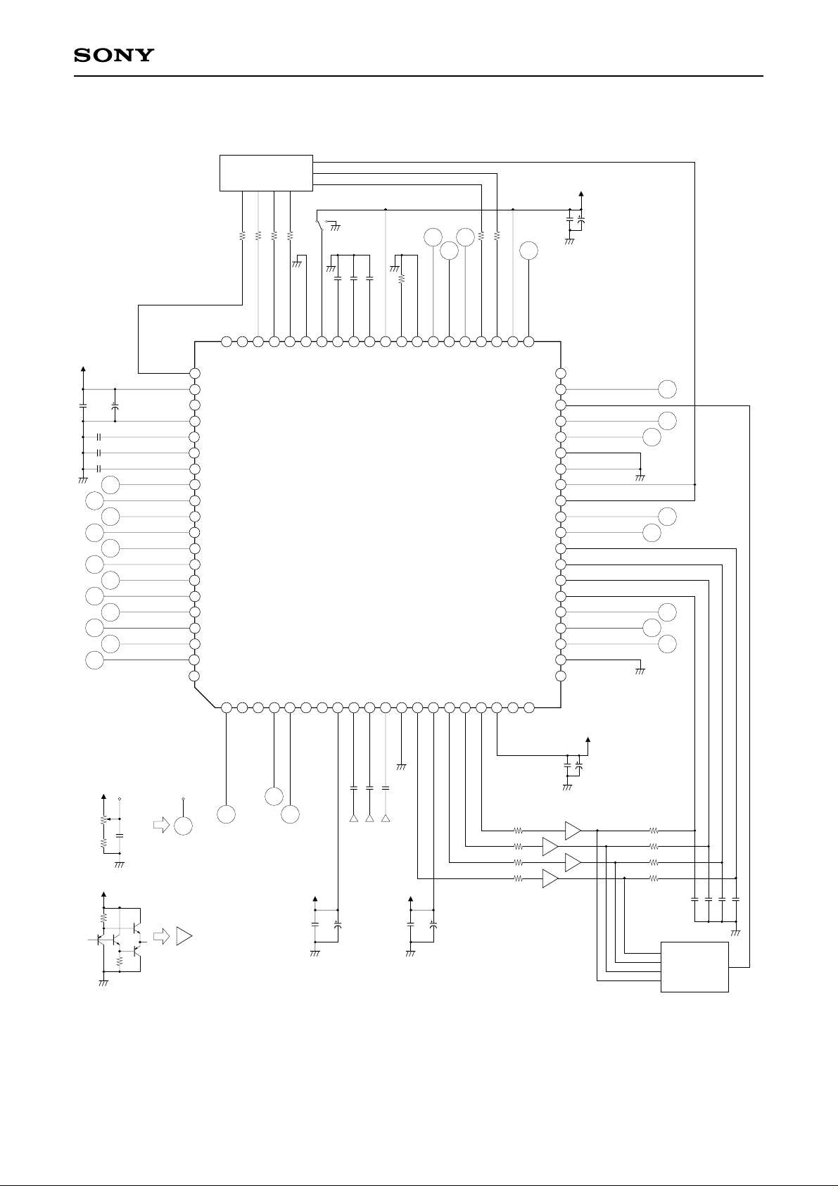
Application Circuit
CXD2412AQ
Timing Generator
100100100100 100100
VR VR
VR VR
CXA1853AQ
5V
0.01µ 100µ
5V
0.01µ 100µ
0.1µ
0.1µ
0.1µ
VR
VR
VR
VR
VR
VR
VR
VR
VR
VR
VR
VR
SH1
PV
SH IN
GND
B CLAMP
G CLAMP
R CLAMP
RGB GAM GAIN1
R GAM GAIN1
B GAM GAIN1
RGB GAM GAIN2
R GAM GAIN2
B GAM GAIN2
RGB GAM CTR2
R GAM CTR2
B GAM CTR2
RGB GAM CTR1
R GAM CTR1
B GAM CTR1
N.C.
0.1µ 0.1µ 0.1µ
N.C.
N.C.
SH2
60
61
CC
62
63
64
65
66
67
68
69
70
71
72
73
74
75
76
77
78
79
80
SH3
57
58
59
SIG SEL
GCA DETR
SH4
GND
55
56
GCA DETG
53
52
54
CXA1853AQ
4
CC
GCA DETB
V
50
51
IREF
49
33k
48
GND
B GAIN
47
R GAIN
46
RGB GAIN
45
XCLP1
44
XCLP2
43
CAM SEL
42
WHT LIM
41
BLK CENT
40
BLK LIM
39
VCOM OUT
38
SIG CENT CTR
37
VCOM CTR
36
PRG
35
GND
34
SID FRP
33
FRP
32
PRG CTR
31
SID CTR
30
SID CLP
29
R CLP
28
G CLP
27
B CLP
26
R SBRT
25
B SBRT
24
RGB SBRT
23
GND
22
N.C.
21
VR
VR
VR
VR
VR
VR
VR
VR
3.3k
3
N.C.
5
4
B MBRT
R MBRT
VR
VRVR
0.01µ 100µ
N.C.
1
2
N.C.
RGB MBRT
5V
68k
0.01µ
33k
13V
3.3k
VR
indicated as VR.
buff
indicated as buff.
6
7
GAM OUT
5V
9
10
8
CC1
RIN
GIN
V
ANALOG
RGB IN
13
12
11
BIN
0.1µG0.1µR0.1µ
B
14 15
GND
SID OUT
13V
0.01µ 100µ
16
CC2
V
R OUT
G OUT
17
B OUT
19
18
20
CC3
N.C.
N.C.
V
150
150
150
150
0.01µ 100µ
buff
buff
buff
buff
5V
390k
390k
390k
390k
LCX007
LCD Panel
Application circuits shown are typical examples illustrating the operation of the devices. Sony cannot assume responsibility for
any problems arising out of the use of these circuits or for any infringement of third party patent and other right due to same.
1µ1µ1µ1µ
– 34 –
Page 35
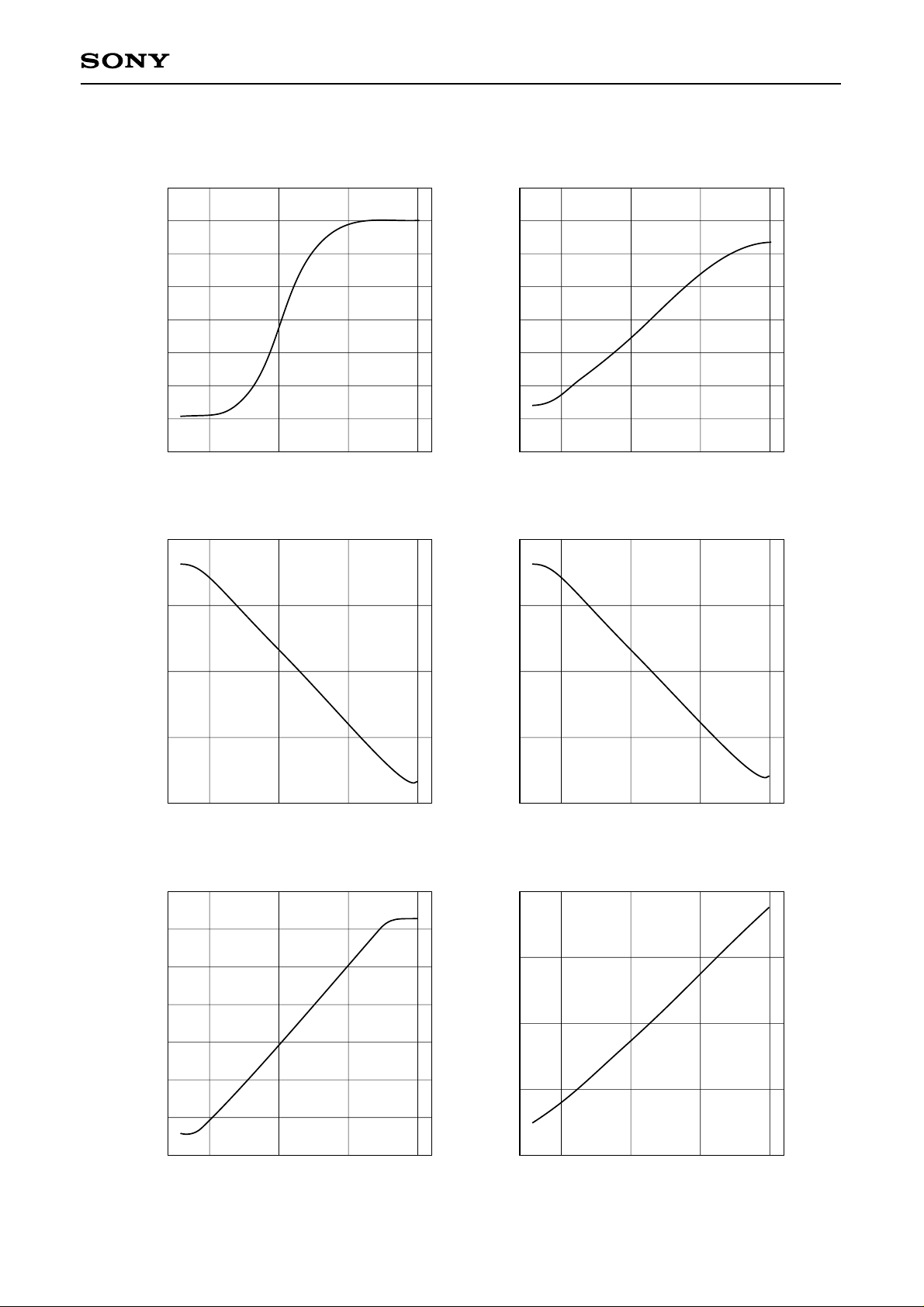
Example of Representative Characteristics
CXA1853AQ
[dB]
CS
∆G
–2
–4
–6
–8
0.4
0.2
RGB GAIN adjustment range
8
6
4
2
0
[dB]
RS
∆G
R GAIN, B GAIN adjustment range
8
6
4
2
0
–2
–4
–6
–8
2543
RGB GAIN (V45) [V]
2543
R GAIN (V46) [V]
B GAIN (V47) [V]
RGB MBRT adjustment range
R MBRT, B MBRT adjustment range
0.2
0.1
[V]
BM
∆V
[V]
SB
V
–0.2
–0.4
12
10
0
[V]
BR
0
∆V
–0.1
–0.2
2543
RGB MBRT (V1) [V]
2543
R MBRT (V4) [V]
B MBRT (V5) [V]
RGB SBRT adjustment range
R SBRT, B SBRT adjustment range
2
[V]
SSR
∆V
1
0
–1
8
6
4
2
–2
0
–2
2543
RGB SBRT (V23) [V]
2543
R SBRT (V25) [V]
B SBRT (V24) [V]
– 35 –
Page 36
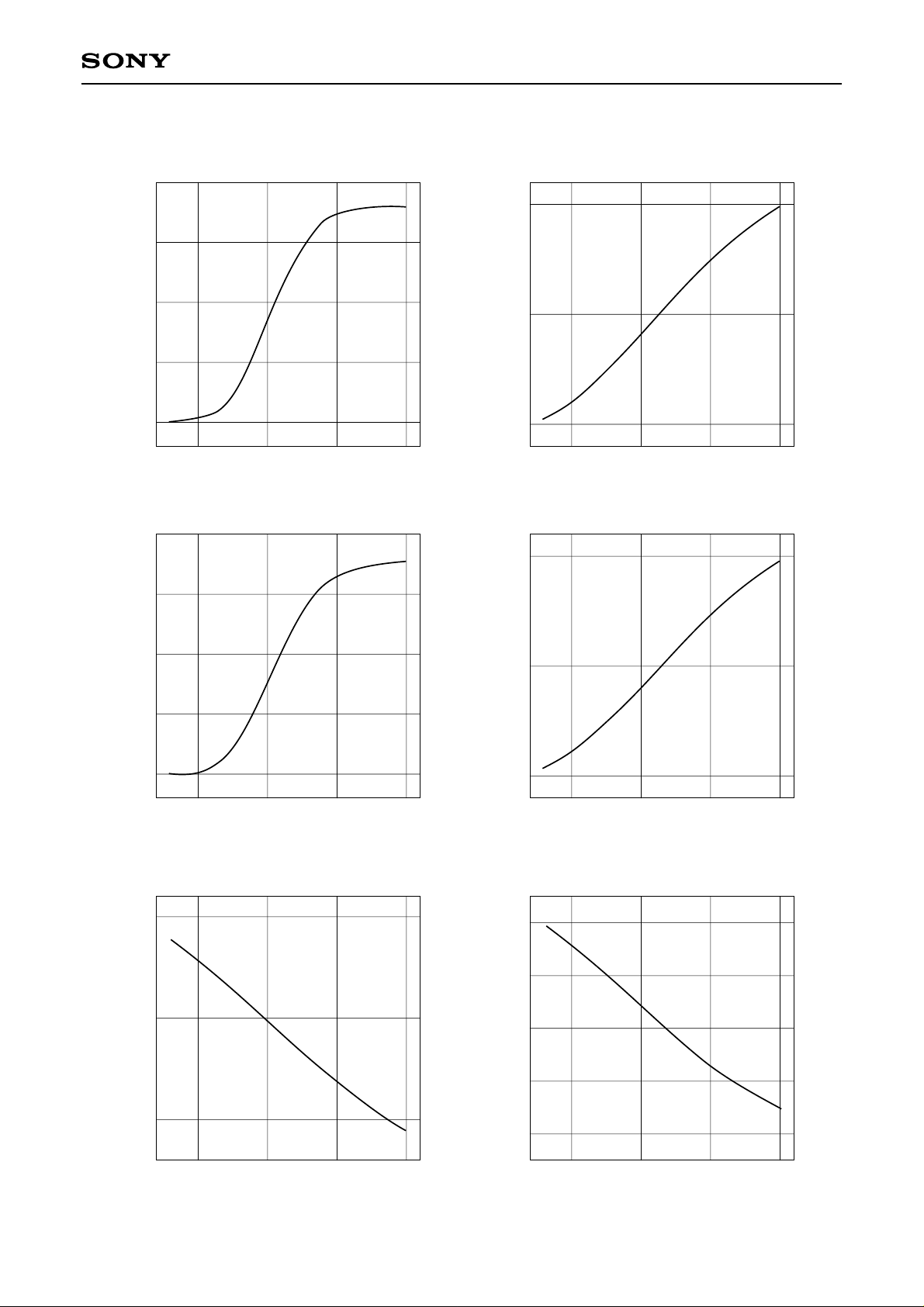
CXA1853AQ
RGB gamma black side gain adjustment range
20
15
10
[dB]
GB
G
5
0
2543
RGB GAM GAIN1 (V68) [V]
RGB gamma white side gain adjustment range
20
15
R, B gamma black side gain adjustment range
5
[dB]
0
GBR
∆G
–5
2543
R GAM GAIN1 (V69) [V]
B GAM GAIN1 (V70) [V]
R, B gamma white side gain adjustment range
5
10
[dB]
GW
G
5
0
2543
RGB GAM GAIN2 (V71) [V]
RGB gamma black side breakpoint
adjustment range
0
–0.5
[V]
GB
P
[dB]
0
GWR
∆G
–5
2543
R GAM GAIN2 (V72) [V]
B GAM GAIN2 (V73) [V]
R, B gamma black side breakpoint sub
adjustment range
0.4
0.2
[V]
0
GBR
∆P
–0.2
–1
2543
RGB GAM CTR1 (V77) [V]
– 36 –
–0.4
2543
R GAM CTR1 (V78) [V]
B GAM CTR1 (V79) [V]
Page 37
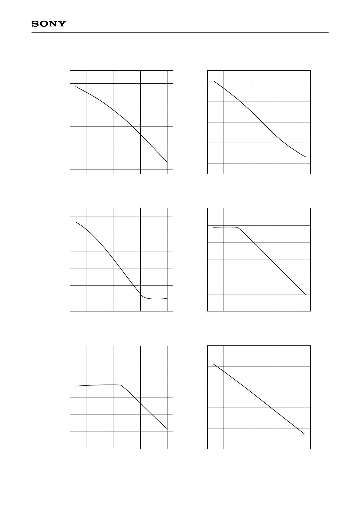
CXA1853AQ
[V]
GW
P
[V]
W
∆V
1.5
0.5
–0.5
–1
–2
RGB gamma white side breakpoint
adjustment range
1
0
2543
RGB GAM CTR2 (V74) [V]
WHT LIM adjustment range
3
2
1
0
2543
WHT LIM (V41) [V]
R gamma white side breakpoint sub
adjustment range
0.4
0.2
[V]
0
GWR
∆P
–0.2
–0.4
2543
R GAM CTR2 (V75) [V]
B GAM CTR2 (V76) [V]
BLK LIM adjustment range
7
6
5
4
(non-inverted side) [V]
BGL
3
– V
CG1
2
V
1
2543
BLK LIM (V39) [V]
BLK LIM adjustment range
7
6
5
4
(inverted side) [V]
CG1
3
– V
BGLA
V
2
1
2543
BLK LIM (V39) [V]
Signal center adjustment range
9
8
7
[V]
C
V
6
5
4
2543
SIG CENT CTR (V37) [V]
– 37 –
Page 38
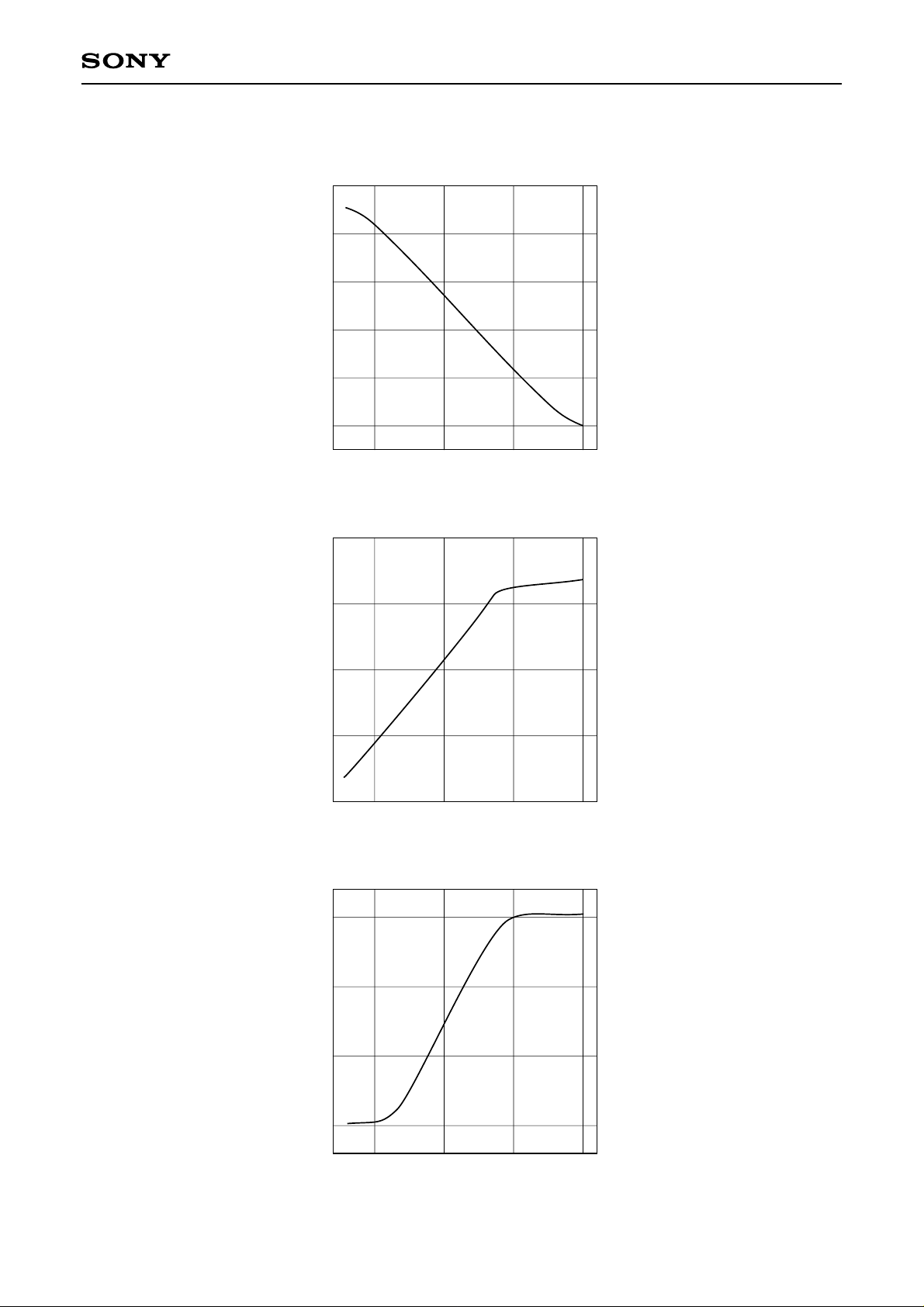
VCOM control range
3
2
1
[V]
COM
0
∆V
–1
–2
2543
VCOM CTR (V36) [V]
CXA1853AQ
SID amplitude control range
12
10
8
[Vp-p]
SID
V
6
4
2543
SID CTR (V30) [V]
PRG level control range
3
2
[Vp-p]
PRG
V
1
0
2543
PRG CTR (V31) [V]
– 38 –
Page 39

Package Outline Unit: mm
80PIN QFP (PLASTIC)
16.0 ± 0.3
14.0 ± 0.2
CXA1853AQ
1.4 ± 0.2
61
80
0.625 ± 0.2
60
0.65
1.70 MAX
0.3 ± 0.05
0.1 ± 0.1
41
201
0.13
40
21
0.1
15.0 ± 0.2
A
M
0.15 ± 0.05
SONY CODE
EIAJ CODE
JEDEC CODE
0° to 10°
DETAIL A
QFP-80P-L111
QFP080-P-1414
PACKAGE STRUCTURE
PACKAGE MATERIAL
LEAD TREATMENT
LEAD MATERIAL
PACKAGE WEIGHT
– 39 –
EPOXY RESIN
SOLDER PLATING
COPPER ALLOY
0.6g
 Loading...