

Page 1
—1—
E97102B8Y
Sony reserves the right to change products and specifications without prior notice. This information does not convey any license by
any implication or otherwise under any patents or other right. Application circuits shown, if any, are typical examples illustrating the
operation of the devices. Sony cannot assume responsibility for any problems arising out of the use of these circuits.
Absolute Maximum Ratings (Ta=25 °C)
• Supply voltage VCC 13 V
• Operating temperature Topr –40 to +85 °C
• Storage temperature Tstg –65 to +150 °C
• Allowable power dissipation
PD SOP 350 (75°C) mW
SSOP 220 (75°C) mW
Recommended Supply Voltage Range
Supply voltage VCC 6 to 12 V
Description
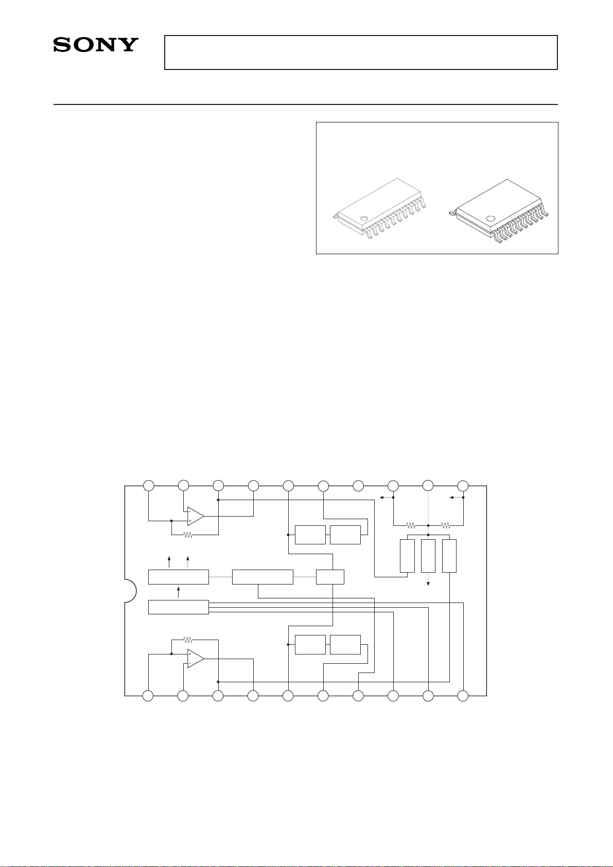
The CXA1846AM/AN is an electrical volume
control IC for use in car radios/stereos and radiocassette recorders featuring serial data control. It
has improved over the CXA1846M/N by reducing
the ‘pop’ noise during volume level-switchings.
Features
• Volume adjustment (0dB to –87dB, – ∞dB)
• Balance
• Serial data control (DATA, CLK, CE)
• Single 8V power supply
• Zero-cross detection circuit
Structure
Bipolar silicon monolithic IC
Electronic volume control
CXA1846AM/AN
Block Diagram and Pin Configuration
VOLUME
8dB STEP
VOLUME
1dB STEP
100k 100k
VCTBUFF
LATCH
SHIFT REGISTER
ZCDETLATCH CONTROL
VOLUME
8dB STEP
VOLUME
1dB STEP
VCTBUFF
VCTBUFF
50K
50K
INP1
INN1
VCT1
INAO1
VRIN1
OUT1
NC
GND
VCT
V
CC
INP2
INN2
VCT2
INAO2
VRIN2
OUT2
CE
DATA
CLK
INIT
1
2
3
4
5
6
7
8
9
10
20
19
18
17
16
15
14
13
12
11
CXA1846AM CXA1846AN
20 pin SOP (Plastic) 20 pin SSOP (Plastic)
For the availability of this product, please contact the sales office.
Page 2
—2—
CXA1846AM/AN
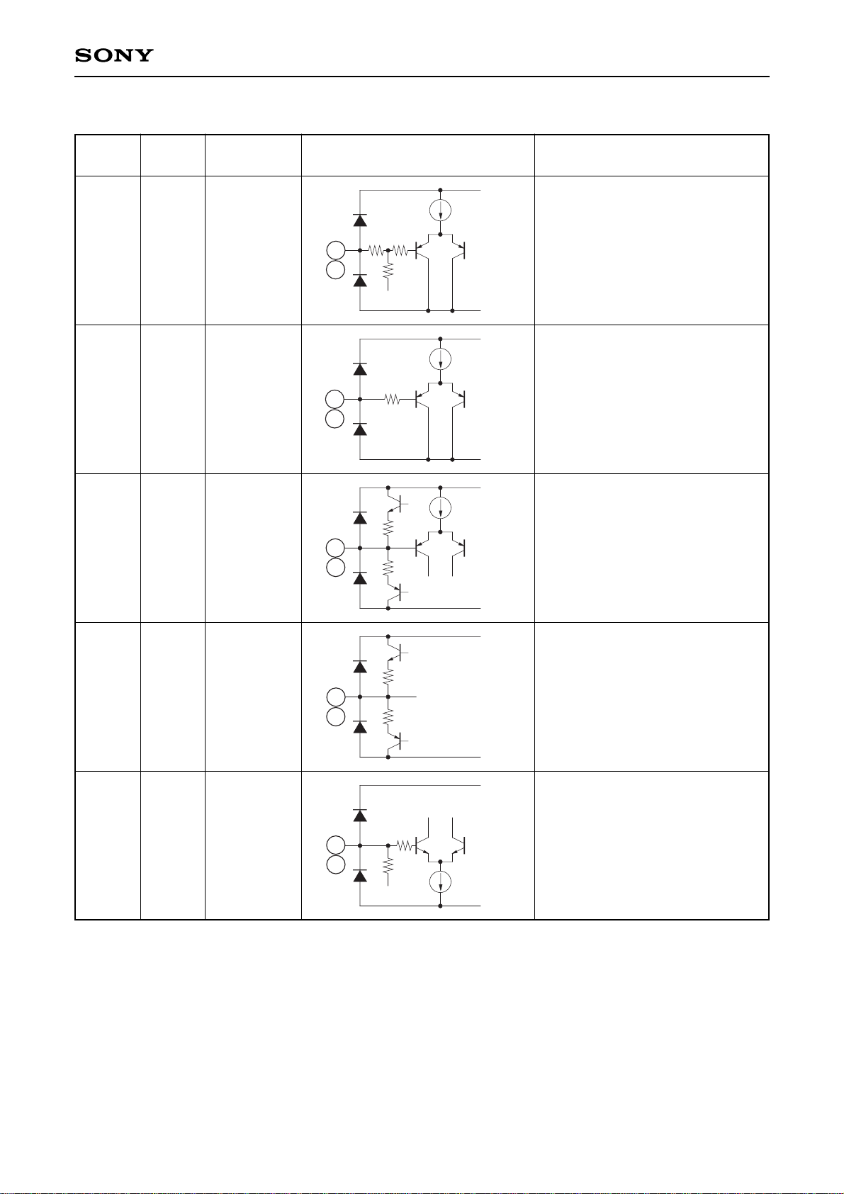
Pin Description
1
20
2
19
3
18
4
17
5
16
INP2
INP1
INN2
INN1
VCT2
VCT1
INAO2
INAO1
VRIN2
VRIN1
50kΩ
VCT
—
VCT
—
VCT
—
VCT
8.2kΩ
VCT
129
V
CC
GND
20
1
129
V
CC
GND
2
19
VCC
GND
18
3
VCC
GND
4
17
VCC
GND
16
5
Input operational amplifier positive
phase input
Input operational amplifier
reversed phase input
VCT buffer output
Input operational amplifier
Volume input
Pin No. Symbol
I/O resistance
voltage
Equivalent circuit Description
Page 3
—3—
CXA1846AM/AN
6
15
7
8
9
10
11
12
13
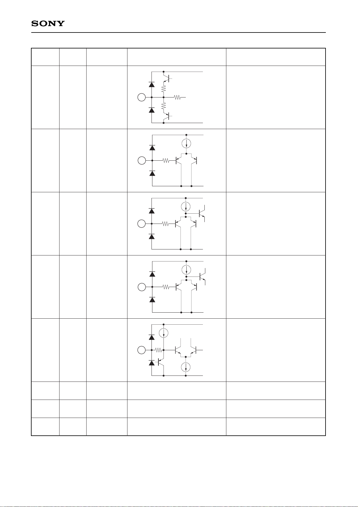
OUT2
OUT1
CE
DATA
CLK
INIT
VCC
VCT
GND
—
VCT
≅ ∞
—
≅ ∞
—
≅ ∞
—
—
—
—
—
VCT
—
—
VCC
GND
6
129
V
CC
GND
7
129
V
CC
GND
8
129
V
CC
GND
9
129
V
CC
GND
10
Volume output
Latch enable
Serial data input
Serial clock
System reset
+ power supply
Mid-point potential
GND
Pin No. Symbol
I/O resistance
voltage
Equivalent circuit Description
Page 4
—4—
CXA1846AM/AN
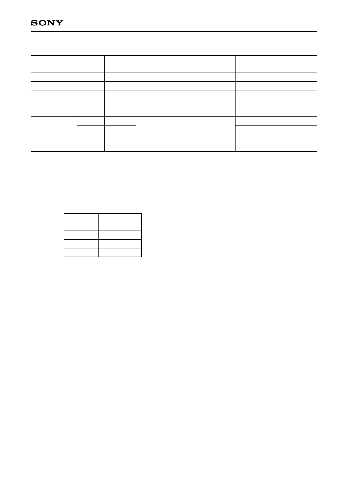
Electrical Characteristics (Unless otherwise specified VCC = 8V, Ta = 25°C)
Item Symbol Measurement Condition Min. Typ. Max. Unit
Circuit current
Total harmonic distortion
Output noise voltage
Maximum output voltage
Separation
Maximum attenuation
Input voltage
High
Low
Input voltage range
Maximum output current
ICC
THD
Vn
Vom
CS
ATTm
Vsh
Vsl
Vin
Imax
No signal
1kHz, 5dBm
Input shorted
1kHz
1kHz
Data, INIT
CLK, CE
Input buffer amplifier output current
5 8 12 mA
— 0.003 0.01 %
— 5 7 µVrms
8 — — dBm
85 90 — dB
85 90 — dB
3 — 6 V
0 — 1.5 V
1 — VCC – 1 V
— — 1 mA
RESET
The IC is reset by reducing the voltage at the INIT pin to 1V or less when CLK is high. Reset can not be
performed when CLK is low. The table below shows the status when the IC has been reset.
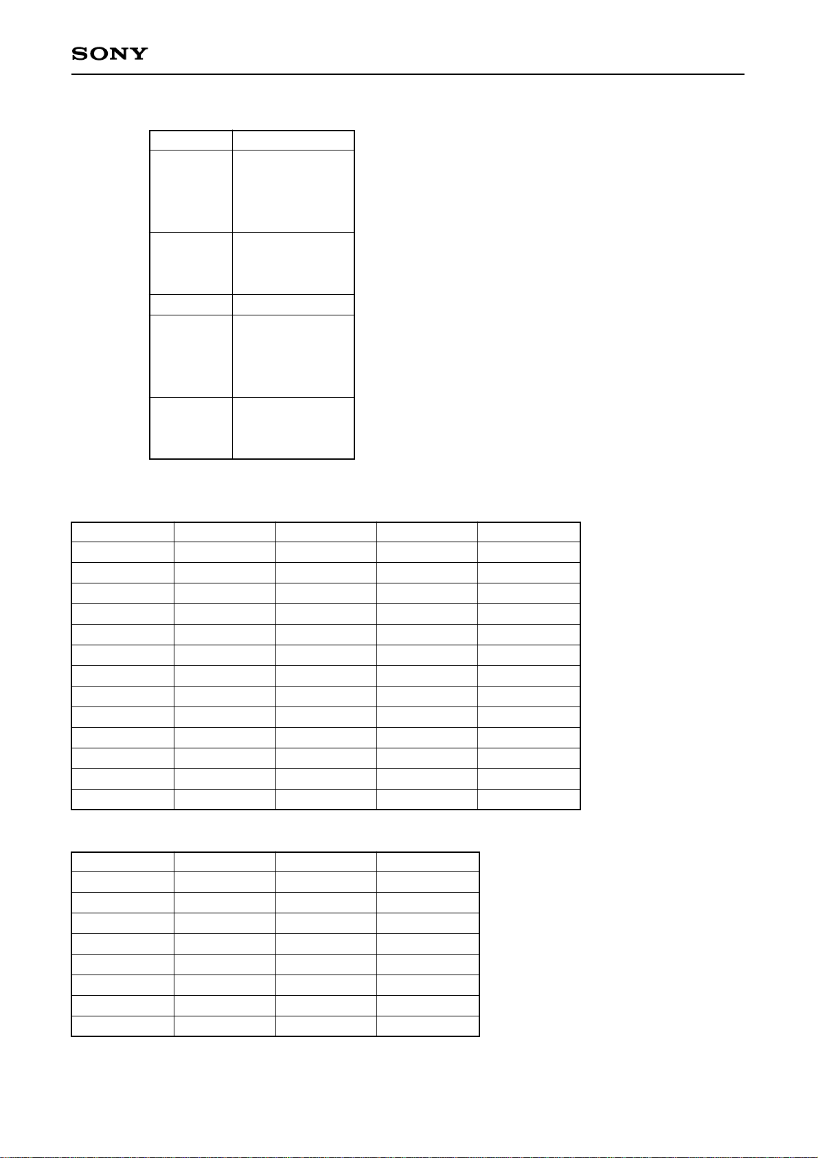
MODE Setting
VRC1 – ∞
VRF1 –7dB
VRC2 – ∞
VRF2 –7dB
Page 5
—5—
CXA1846AM/AN
D1
D2
D3
D4
D5
D6
D7
D8
D9
D10
D11
D12
D13
D14
D15
D16
NOP
VRC1
VRF1
NOP
VRC2
VRF2
Fast bit MSB
LSB
Data Allocation
VRC1/VRC2
VRF1/VRF2
Setting
0
–8
–16
–24
–32
–40
–48
–56
–64
–72
–80
– ∞
– ∞
D2/D10
1
1
1
1
1
1
1
1
0
0
0
0
0
D3/D11
1
1
1
1
0
0
0
0
1
1
1
1
0
D4/D12
1
1
0
0
1
1
0
0
1
1
0
0
0
D5/D13
1
0
1
0
1
0
1
0
1
0
1
0
0
Setting
0
–1
–2
–3
–4
–5
–6
–7
D6/D14
1
1
1
1
0
0
0
0
D7/D15
1
1
0
0
1
1
0
0
D8/D16
1
0
1
0
1
0
1
0
Page 6
—6—
CXA1846AM/AN
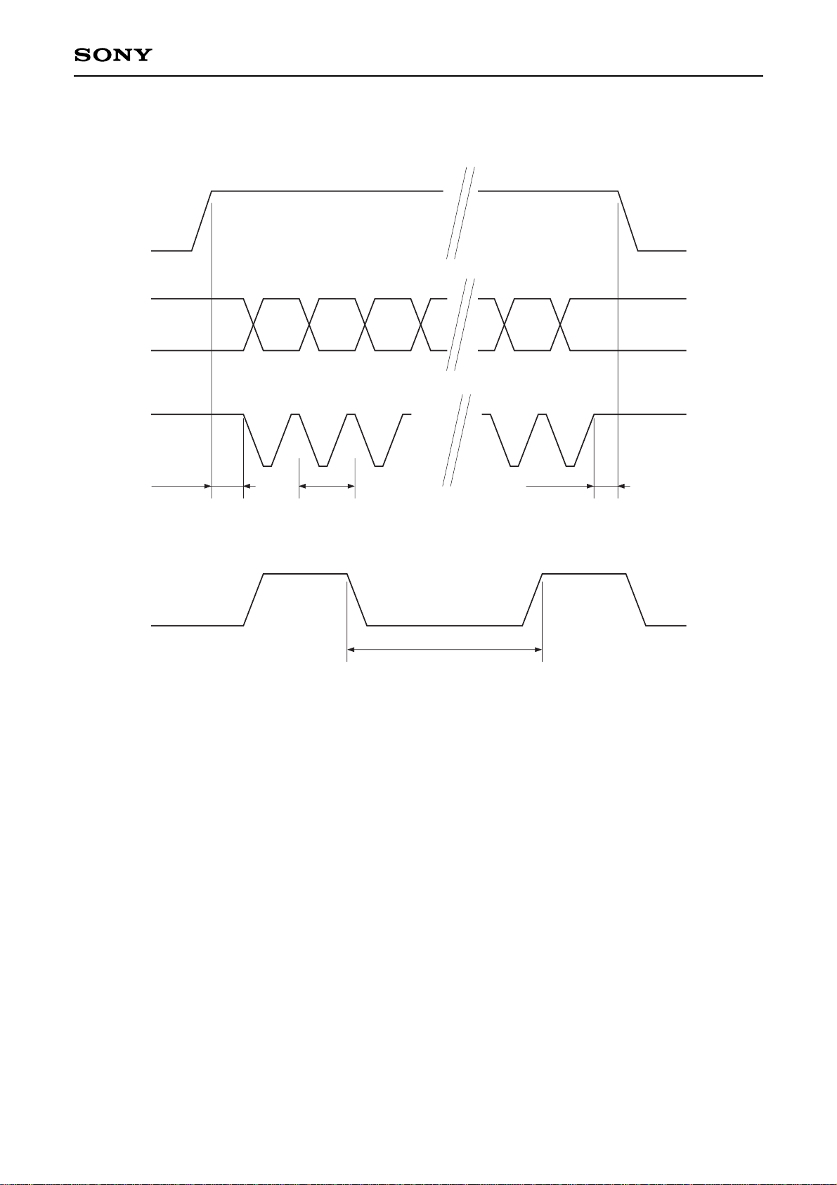
Data Timing
Min. 0.5µs
Max. 1MHz
Min. 0.5µs
Min. 4µs
CE
DATA
CLK
CE
D1 D2 D3 D15 D16
Page 7

—7—
CXA1846AM/AN
Test Circuit
INP1
INN1
VCT1
INAO1
VRIN1
OUT1
NC
GND
VCT
V
CC
INP2
INN2
VCT2
INAO2
VRIN2
OUT2
CE
DATA
CLK
INIT
C2
10µ
V2
AC
GND
R3
1k
R4
1k
V4
50mV
TP1 TP2
S1
S2
S3
C4
10µ
S4
A
B
100p
C6
10k
R6
GND
TP3
C7
10µ
C9
1µ
R8
10k
GND
V6
AC
–60dBm
GND
V7
8V
V
CC
C1
10µ
V1
AC
GND
R2
1k
R1
1k
50mV
V3
TP4 TP5
S5
S6
S7
C3
10µ
S8
A
B
100p
C5
10k
R5
C8
1µ
R7
10k
GND
V5
AC
–60dBm
GND
C10
1n
1k
1k
1k
CLK
DATA
CE
5V
0V
5V
0V
5V
0V
1
2
3
4
5
6
7
8
9
10
11
12
13
1415
16
17
18
19
20
Page 8

—8—
CXA1846AM/AN
Application Circuit
INP1
INN1
VCT1
INAO1
VRIN1
OUT1
NC
GND
VCT
V
CC
INP2
INN2
VCT2
INAO2
VRIN2
OUT2
CE
DATA
CLK
INIT
C2
10µ
10µ
C5
IN1
R4
10k
R4
10k
OUT1
10µ
C7
GND
10µ
C8
GND
47µ
C10
VCC
C1
IN2
10µ 10µ
R4
R3
10k
R1
10k
OUT2
10µ
C6
GND
SERIAL CTL
C11
0.01µ
1
2
3
4
5
6
7
8
9
10
11
12
13
14
15
16
17
18
19
20
Application circuits shown are typical examples illustrating the operation of the devices. Sony cannot assume responsibility for
any problems arising out of the use of these circuits or for any infringement of third party patent and other right due to same.
Page 9
—9—
CXA1846AM/AN
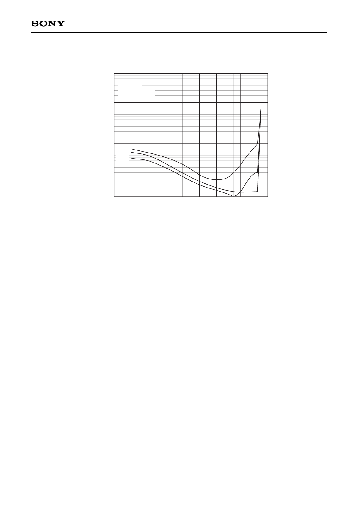
Total harmonic distortion
Output level [dBm]
1.0
0.1
0.01
0.001
Total harmonic distortion [%]
–30 –20 –10 0 2 4 6 8 10
RL = 10kΩ
VCC = 8V
Volumue = 0dB
20kHz
100Hz
1kHz
Page 10
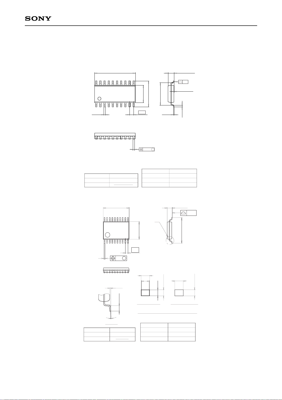
Package Outline Unit : mm
CXA1846AM/AN
—10—
CXA1846AM
SONY CODE
EIAJ CODE
JEDEC CODE
SOP-20P-L01
SOP020-P-0300
PACKAGE STRUCTURE
PACKAGE MATERIAL
LEAD TREATMENT
LEAD MATERIAL
PACKAGE MASS
COPPER ALLOY
SOLDER PLATING
EPOXY RESIN
0.3g
20PIN SOP (PLASTIC)
12.45 – 0.1
+ 0.4
20
11
0.45 ± 0.1
1.27
10
1
5.3 – 0.1
+ 0.3
7.9 ± 0.4
6.9
0.2 – 0.05
+ 0.1
0.5 ± 0.2
0.1 – 0.05
+ 0.2
1.85 – 0.15
+ 0.4
0.15
0.24
M
CXA1846AN
20PIN SSOP (PLASTIC)
SONY CODE
EIAJ CODE
JEDEC CODE
PACKAGE STRUCTURE
PACKAGE MATERIAL
LEAD TREATMENT
LEAD MATERIAL
PACKAGE MASS
EPOXY RESIN
SOLDER / PALLADIUM
42/COPPER ALLOY
0.1g
SSOP-20P-L01
SSOP020-P-0044
PLATING
0.1 ± 0.1
0.5 ± 0.2
0° to 10°
DETAIL A
NOTE: Dimension “∗” does not include mold protrusion.
b=0.22 – 0.05
+ 0.1
0.15 – 0.02
+ 0.05
(0.22)
(0.15)
0.15 – 0.01
DETAIL B : SOLDER DETAIL B : PALLADIUM
+ 0.03
b=0.22 ± 0.03
∗6.5 ± 0.1
∗4.4 ± 0.1
0.65
20
11
10
1
A
0.1
1.25 – 0.1
+ 0.2
6.4 ± 0.2
0.13
M
b
NOTE : PALLADIUM PLATING
This product uses S-PdPPF (Sony Spec.-Palladium Pre-Plated Lead Frame).
 Loading...