

Page 1
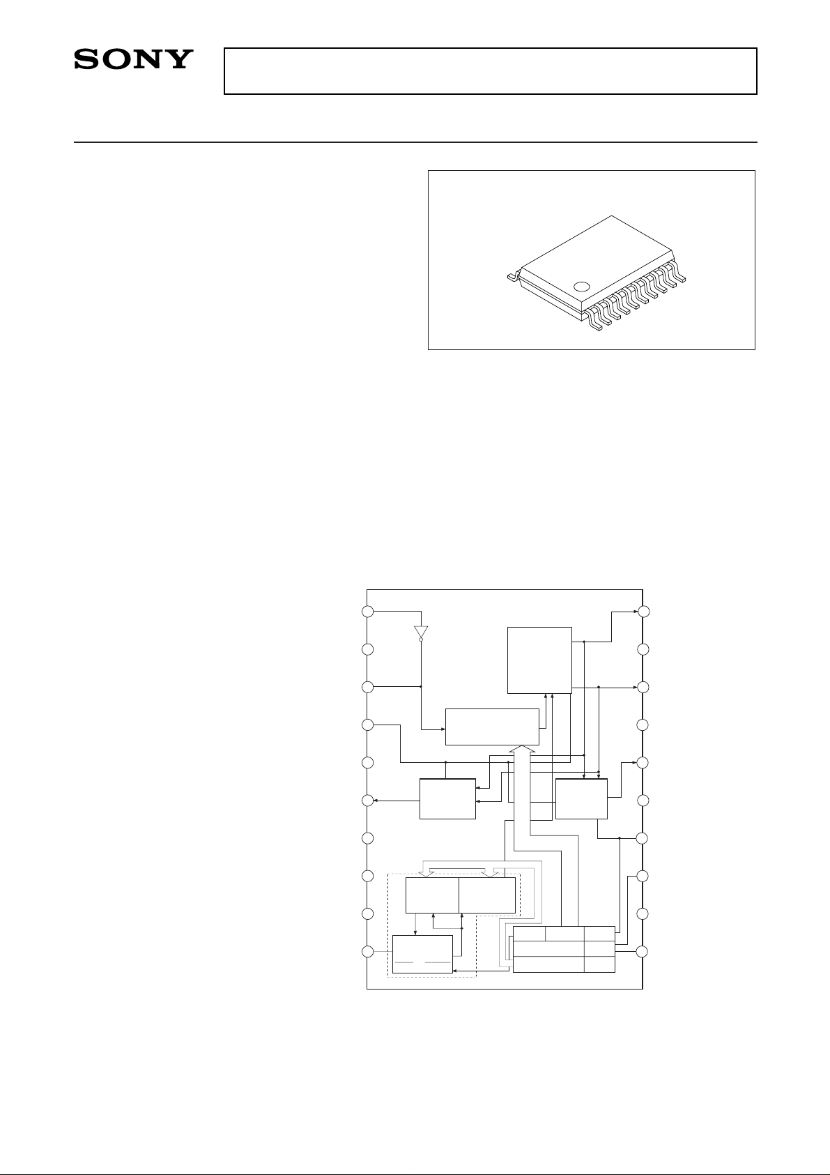
1.1GHz-band PLL IC for Mobile Communications
Descriptions
The CXA1786N is a frequency synthesizer PLL IC
developed for use in mobile communication systems.
This IC has low current consumption, small package
and is suitable for portable sets of cellular telephone
and others.
Features
• Low current consumption
Icc = 6.0mA (typ.)
0.3mA (typ.) in power saving mode
• Maximum operating frequency
1.1GHz guaranteed
• Operating supply voltage range
2.7 to 5.5V
• Ultra small 20-pin SSOP package
• Two types of phase comparator output:
For external charge pump φR φP
Two internal charge pumps DO1DO2
Applications
1.1GHz-band mobile communication equipment
such as cellular telephones
Structure
Bipolar silicon monolithic IC
Absolute Maximum Ratings
• Supply voltage Vcc 7 V
• Operating temperature Topr –35 to +85 °C
• Storage temperature Tstg –65 to +150 °C
• Allowable power dissipation
PD 300 mW
Operating Condition
Supply voltage Vcc 2.7 to 5.5 V
– 1 –
E93929A8Y
Sony reserves the right to change products and specifications without prior notice. This information does not convey any license by
any implication or otherwise under any patents or other right. Application circuits shown, if any, are typical examples illustrating the
operation of the devices. Sony cannot assume responsibility for any problems arising out of the use of these circuits.
CXA1786N
Reference Programmable
Counter 14bits
Charge
Pump 2
Phase
Comparator
OSCI
NC
OSCO
Vp
VCC
DO1
GND
LD
NC
FIN
φR
NC
φP
TEST
D
O2
FC
LAT
DATA
PS
CK
2
5
7
8
9
12
15
17
18
19
1
Charge
Pump 1
Pulse Swallow
Counter 7bits
Programmable
Counter 11bits
2-modulus
prescaler
64/65
1
128/129
1
or
14-bit Latch
1-bit Latch
1-bit Shift
Resister
18-bit Latch
4
6
10
11
13
14
Pulse swallow programmable counter
20
16
18-bit Shift Resister
3
20 pin SSOP (Plastic)
Block Diagram and Pin Configuration
For the availability of this product, please contact the sales office.
Page 2
– 2 –
CXA1786N
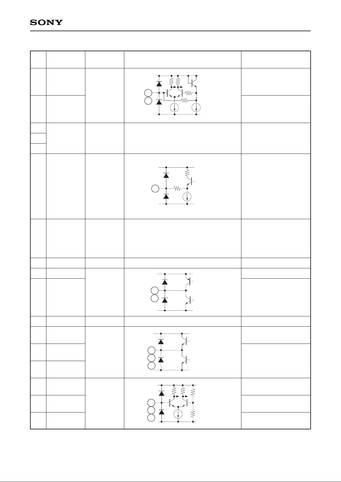
Pin Description
Pin
No.
Symbol
Typical pin
voltage (DC)
Equivalent circuit Description
Reference frequency
signal input.
VCO signal input.
No connected.
Reference frequency
signal output.
Oscillator is formed by
connecting the crystal
resonator between this
pin and the OSCI pin; the
oscillator signal is used
as the reference
frequency signal.
Power supply for the
charge pump outputs
(Do1, Do2) and phase
comparator outputs
(φR, φP).
Power supply.
1
10
2
9
19
3
4
5
6
16
7
8
18
20
11
13
14
OSCI
FIN
NC
OSCO
VP
VCC
DO1
DO2
GND
LD
φP
φR
CK
DATA
LAT
Charge pump 1 output.
Charge pump 2 output.
Outputs only when the
LAT pin is High; in high
impedance when the
LAT pin is Low.
Ground.
Lock detection signal
output.
Clock input.
Data input.
Latch input.
Open Low
—
—
3V
High: 2.2V
Low: 2.0V
—
2.2V
—
—
High: 2.2V
Low: 0.1V
Phase comparator output.
Used for the external
charge pump.
VCC
GND
10
1
VCC
GND
3
500Ω
GND
6
16
Vp
Vp
GND
8
18
20
(LD is VCC)
VCC
GND
11
13
14
3V
—
Page 3
– 3 –
CXA1786N
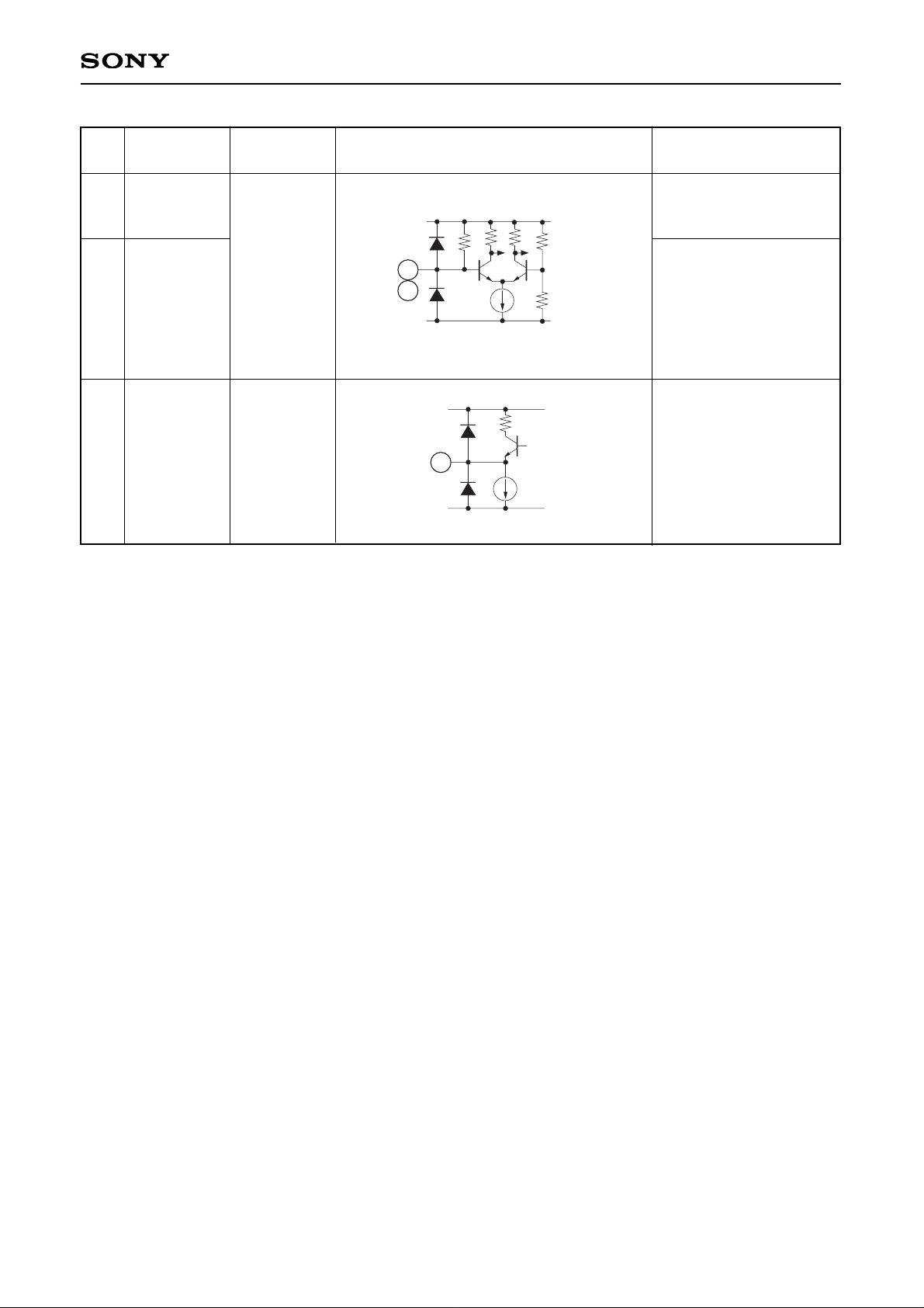
Pin
No.
Symbol
Typical pin
voltage (DC)
Equivalent circuit Description
Power saving pin.
Power saving mode
when this pin is Low.
Switching for the phases
of phase comparator
output and the output
signals of counter
(reference,
programmable) output to
the TEST pin.
The signal output which
is frequency-divided at
the counter.
12
15
PS
FC
Open High
17
TEST
High: 2.2V
Low: 2.0V
VCC
GND
12
15
17
Page 4
– 4 –
CXA1786N
Item
Current consumption
Current consumption
(in power saving mode)
FIN operating frequency
FIN input level
OSCI operating frequency
OSCI input level
DO1
High output current
DO2
DO1
Low output current
DO2
DO1 High impedance
DO2 leak current
(leak current DO2 off)
φR
φP High output voltage
LD
φR
φP Low output voltage
LD
CK
DATA
LAT
PS
PS
High input voltage
High input current
Low input voltage
Low input current
Low input current
Icc
Icc
(PS)
fin
Pin
fosc
Vosc
IOH
IOL
IOZ
VOH
VOL
VIH
IOH
VIL
IIL
IIL
Vcc = Vp = 2.7V to 5.5V
Ta = –35°C to +85°C
Vcc = Vp = 2.7V to 5.5V
Ta = –35°C to +85°C
Vcc = Vp = 2.7V to 5.5V
Ta = –35°C to +85°C
Vcc = Vp = 2.7V to 5.5V
Ta = –35°C to +85°C
IL = 0.1mA
IL = 0.1mA
VIN = Vcc
VIN = GND except for PS
VIN = GND
100
–10
5
0.5
1
–1
2
Vcc × 0.7
–1
–1
–30
5.84
360
2.18
70.3
–15.5
8.7
510
1100
10
20
2
–1
1
500
1
Vcc × 0.3
1
mA
µA
MHz
dBm
MHz
Vpp
mA
mA
µA
V
mV
V
µA
V
µA
µA
Symbol Conditions Min. Typ. Max. Unit
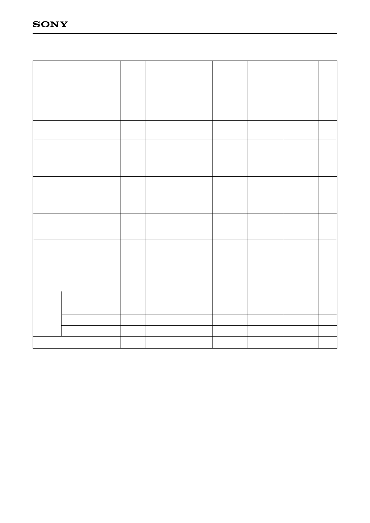
Electrical Characteristics
(Vcc = Vp = 3V, Ta = 25°C, refer to the Electrical Characteristics Measurement Circuit)
Page 5

– 5 –
CXA1786N
Item
PS
High input voltage
High input current
Low input voltage
Low input current
High input voltage
High input current
Low input voltage
Low input current
Low input current
High input voltage
High input current
Low input voltage
Low input current
FC
CK
DATA
LAT
PS
FC
VIH
IIH
VIL
IIL
VIH
IIH
VIL
IIL
IIL
VIH
IIH
VIL
IIL
VIN = Vcc
VIN = GND
Vcc = VP = 5.5V
Vcc = VP = 5.5V,
VIN = Vcc
Vcc = VP = 5.5V
Vcc = VP = 5.5V,
VIN = GND except for PS
Vcc = VP = 5.5V,
VIN = GND
Vcc = VP = 5.5V
Vcc = VP = 5.5V,
VIN = Vcc
Vcc = VP = 5.5V
Vcc = VP = 5.5V,
VIN = GND
Vcc – 0.05
–1
–50
Vcc × 0.7
–1
–20
–60
Vcc – 0.05
–1
–60
–18.9
0
–27.7
–34.7
1
0.05
1
1
Vcc × 0.3
1
1
0.05
1
V
µA
V
µA
V
µA
V
µA
µA
V
µA
V
µA
Symbol Conditions Min. Typ. Max. Unit
Page 6

– 6 –
CXA1786N
Electrical Characteristics Measurement Circuit
Application Circuit
φR
NC
φP
TEST
D
O
2
FC
LAT
DATA
PS
CK
OSCI
NC
OSCO
VP
Vcc
D
O
1
GND
LD
NC
FIN
CXA1786N
S.G.
51
1000p
51
1000p
S.G.
51
1000p
51
2
3
4
5
7
9
10
11
17
19
1
6
8
V
20
18
A
12
13
14
Controller
15
A
16
OUT
Oscilloscope
Frequency
Counter
5.1k
V
V
V
A
A
A
A
A
1µ
+
1000p
1µ
+
A
A
φR
NC
φP
TEST
D
O
2
FC
LAT
DATA
PS
CK
OSCI
NC
OSCO
VP
Vcc
D
O
1
GND
LD
NC
FIN
CXA1786N
1000p
2
3
7
9
10
11
17
19
1
8
20
18
13
1415
16
TCXO
4
5
1000p
51
L.P.F. V.C.O. Output
12
Power save
LAT
DATA
CK
Controller
1k
1k
1k
1k
6
1000p
+
1µ
1000p
Application circuits shown are typical examples illustrating the operation of the devices. Sony cannot assume responsibility for
any problems arising out of the use of these circuits or for any infringement of third party patent and other right due to same.
Page 7

– 7 –
CXA1786N
Description of Operation
1. Data Setting Method
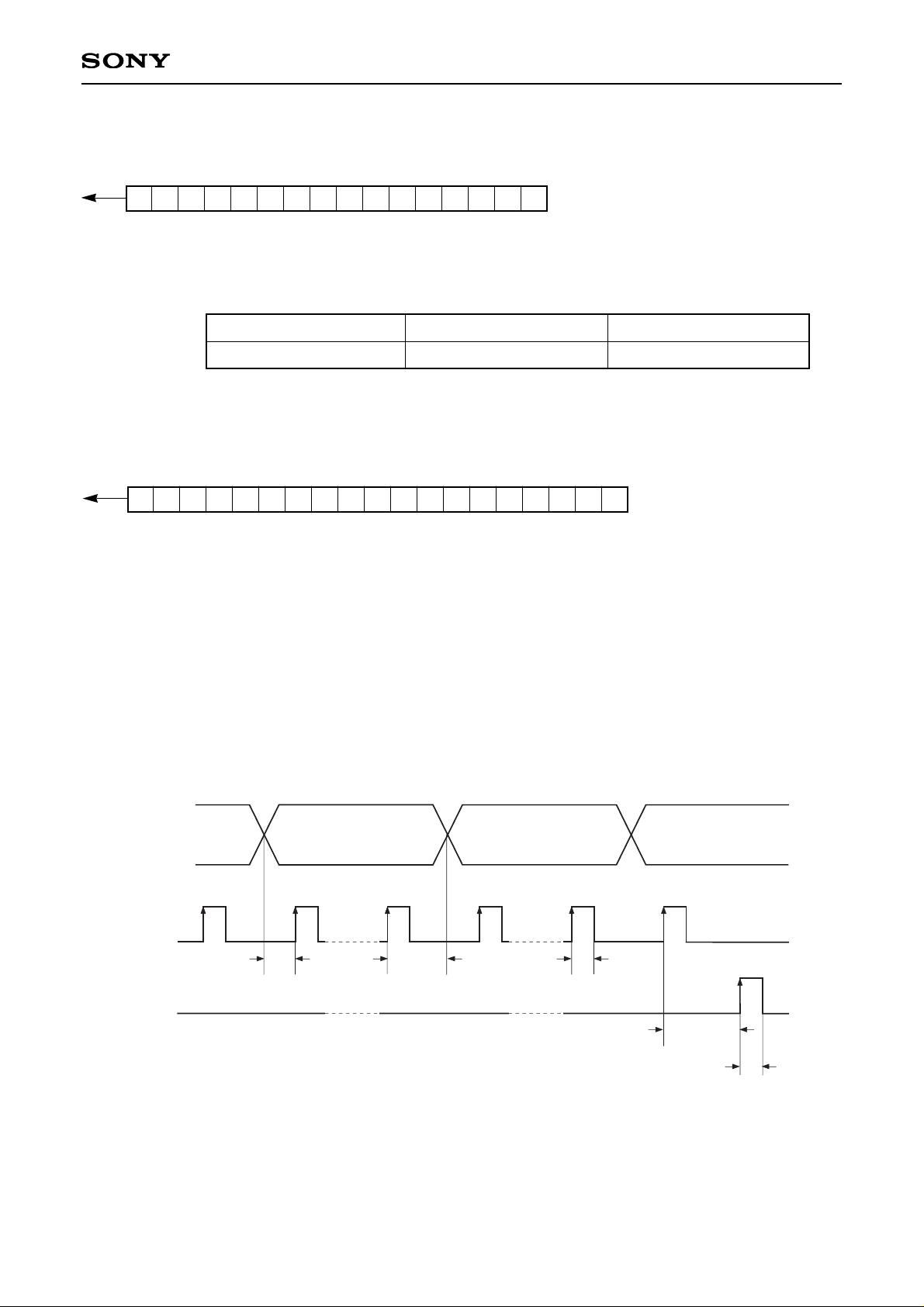
The data is set using three signals — CK, DATA, and LAT in this IC.
In that case, the serial data as described below is input.
(1) Data input method
The 15 bits of data should be input to the reference counter latch and the 18 bis of data to the pulse swallow
programmable counter latch to set the all initializing state in this IC. Every one bit of data is retrieved into the
shift resister at the rising edge of clock input to the CK pin when the data is input to the DATA pin. The input
data is retrieved into the reference counter latch or the pulse swallow programmable counter latch according to
the state of the final bit C.
The data is latched when the latch pulse is input to the LAT pin after 16 bits of data or 19 bits of data, which
were added with the bit C, are sent to the shift resister.
For actual use, first input the 16 bits (including the frequency division setting bit SW for 2-modulus prescaler) of
reference counter data from the controller as indicated above. In this time, set the final bit C High.
Next, input the 19 bits of pulse swallow programmable counter data in the same way. In this time, set the final
bit C Low. Then, all of the interior state has been set. Hereafter, when only the programmable counter data is
to be changed, only the latter 19 bits of programmable counter data should be changed. (In this case, set the
bit C Low.)
(2) Control data construction
The control data consists of 16 bits for the reference counter and 19 bits for the pulse swallow programmable
counter. The final bit of them is the identification code and the contents of data are discriminated by identifying
the code. The frequency division value is composed of the binary values whose head is MSB as described on
the next page.
Page 8
– 8 –
CXA1786N
(a) Data structure of reference counter
(First, input the SW bit and input the C bit last.)
R0 to RD: Frequency division number of reference counter (Binary value with R0 as LSB)
SW: Switching bit of frequency division numbers of 2-modulus pre-scaler block for programmable
counter.
C: This code decides the latch direction of data; set to High.
(b) Data structure of pulse swallow programmable counter
(First, input the MA bit and input the C bit last.)
M0 to MA: Frequency division number of main counter (Binary value with M0 as LSB)
S0 to S6: Frequency division number of swallow counter (Binary value with S0 as LSB)
C: This code decides the latch direction of data; set to Low.
The frequency division value of programmable counter can be obtained with the following equation;
N × M + S N: Frequency division value of 2-modulus pre-scaler (64 or 128)
(M > S) M: Main counter value
S: Swallow counter value
(1) Data input timing
SW RD RC RB RA R9 R8 R7 R6 R5 R4 R3 R2 R1 R0 C
Input direction
MA M9 M8 M7 M6 M5 M4 M3 M2 M1 M0 S6 S5 S4 S3 S2 S1 S0 C
Input direction
SW
Frequency division number164/65-frequency division0128/129-frequency division
DATA
CK
LAT
(C bit)
Data is read at the rising edge of CK.
t1 to t5 ≥ 500ns
(SW bit or MA bit)
t1 t2 t3
t5
t4
Page 9

– 9 –
CXA1786N
FC: High or open
Do1 (2)
φR φP
TEST
Do1 (2)
φR φP
TEST
FC: Low
fr > fp
fr = fp
fr < fp
H
Z
L
L
L
H
L
H
H
fr
fr
fr
L
Z
H
H
L
L
H
H
L
fp
fp
fp
2. Power Save Pin (PS)
This pin is left High when it is open and in power saving mode at Low.
All circuits except for reference counter latch and pulse swallow programmable counter latch are set to off in
the power saving mode. At that mode, Do1 and Do2 are high impedance and the data cannot be set.
∗
The data of reference counter and programmable counter are hold in power saving mode.
3. Do1 and Do2 Pins
These are the charge pump output pins. Do1 operates always. Do2 operates only when the LAT pin is High ; it
is in high impedance state when the LAT pin is Low.
4. FC Pin
This pin switches the charge pump outputs (Do1, Do2) and the phases of phase comparator outputs (φP, φR).
(Refer to the Table 1.)
5. TEST Pin
This pin is for monitoring the counter output signal. The reference counter output and the pulse swallow
programmable counter output are switched according to the FC state as shown at Table 1.
This pin is emitter follower output High level = Vcc – Vf and Low level = Vcc – Vf – 200mV (200mV amplitude).
The DC bias current is decreased to save the power consumption so that the amplitude may not be monitored
for monitoring the waveforms with oscilloscope. In that case, connect the TEST pin to ground with an
approximately 5kΩ resistor.
∗
Z: High impedance fr: Output frequency of reference counter
H: High fp: Output frequency of programmable counter
L: Low
Table 1. Phase comparator and TEST Pin outputs
Page 10

– 10 –
CXA1786N
6. Reference signal (the input signal of reference counter)
The external oscillator signal can be used as the reference signal by inputting the signal of the external
oscillator to the OSCI pin, and the reference signal can be also generated by connecting the crystal resonator
to the OSCI and OSCO pins.
(1) Generation of the reference signal by the external oscillator
Input the signal to the OSCI pin via a capacitor as shown below when the external oscillator signal is use as
the reference signal.
(2) Generation of the reference signal by the built-in oscillator
Connect the crystal resonator between OSCI and OSCO pins as shown below. Use the crystal resonator of
several MHz and confirm the stability of the oscillation and others. The capacitance ratio of CI and Co
should be 1 to 2:1, and their values should be selected so that the serial capacitance of CI and Co may be
the load capacitance specified by the crystal vibrator.
Notes on Operation
• Be careful to use this IC because the electrostatic resistance is the rank "A" due to handling the higher
frequency signal of 1GHz
• Make the input route of the RF signal from the VCO as short as possible.
• Connect the Vcc and Vp pins to the ground respectively via the by-pass capacitors as short as possible
because the frequency of signal used in this IC is higher.
1
2
3
OSCI NC OSCO
1
2
3
OSCI NC OSCO
CI CO
Page 11

– 11 –
CXA1786N
Example of Representative Characteristics
7
6
5
4
3
2
–35 –25 0 25 85
ICC vs. Ta
Ta [°C]
I
CC
(current of V
CC
and Vp) [mA]
ICC vs. VCC
Ta = 25°C
2.7 3 4 5 5.5
6
5
4
3
2
7
I
CC
(current of V
CC
and Vp) [mA]
VCC and Vp voltage [V]
Vcc = 3V
25°C
85°C
35°C
10 100 1000
FIN input level vs. Input frequency
FIN input level [dBm]
FIN input frequency [MHz]
10
0
–10
–20
–30
–40
–50
–60
–70
Vcc = 3V
25°C
85°C
35°C
10
0
–10
–20
–30
–40
1 10 100
OSCI input level vs. Input frequency
OSCI input level [dBm]
OSCI input frequency [MHz]
Vcc, Vp
5V
Vcc, Vp
3V
Page 12

– 12 –
CXA1786N
Package Outline Unit: mm
20PIN SSOP (PLASTIC)
SONY CODE
EIAJ CODE
JEDEC CODE
PACKAGE STRUCTURE
PACKAGE MATERIAL
LEAD TREATMENT
LEAD MATERIAL
PACKAGE MASS
EPOXY RESIN
SOLDER / PALLADIUM
42/COPPER ALLOY
0.1g
SSOP-20P-L01
SSOP020-P-0044
0.1 ± 0.1
0.5 ± 0.2
0° to 10°
DETAIL A
PLATING
∗6.5 ± 0.1
∗4.4 ± 0.1
0.22 – 0.05
+ 0.1
0.65
20
11
10
1
A
0.1
+ 0.05
1.25 – 0.1
+ 0.2
0.15 – 0.02
6.4 ± 0.2
NOTE: Dimension “∗” does not include mold protrusion.
0.13
M
NOTE : PALLADIUM PLATING
This product uses S-PdPPF (Sony Spec.-Palladium Pre-Plated Lead Frame).
 Loading...