

Page 1

Description
The CXA1726AM/AS is a multiplier IC which is
used for dynamic convergence, dynamic focus and
others in CRT display monitors and projectors. It is
used in conjunction with an IC (CXA1470AM/AS)
which generates waveforms for deflection
compensation.
Features
Analog multiplier 4ch
• Maximum input voltage ±1.3V
• Maximum output voltage ±2.7V (RL = 3.9kΩ)
• Frequency response 1.0MHz (–3dB)
• 4 inputs, 1 output 2ch
• 2 inputs, 1 output 2ch
Operational amplifier 2ch
• Maximum output voltage ±3.65V (RL = 1kΩ)
• Frequency response 1MHz (–3dB)
Analog switch 1ch
• Maximum output voltage
• Frequency response
Absolute Maximum Ratings
• Supply voltage VCC 7V
VEE –7 V
• Operating temperature Topr –20 to +75 °C
• Storage temperature Tstg –65 to +150 °C
• Allowable power dissipation PD (CXA1726AM) 625 mW
(CXA1726AS) 1350 mW
Block Diagram and Pin Configuration (Top View)
Applications
• CRT display monitors
• Projectors
Structure
Bipolar silicon monolithic IC
Operating Condition
Supply voltage VCC 5 ± 0.25 V
VEE –5 ± 0.25 V
– 1 –
CXA1726AM/AS
E94607B7X
Multiplier IC for Displays
Sony reserves the right to change products and specifications without prior notice. This information does not convey any license by
any implication or otherwise under any patents or other right. Application circuits shown, if any, are typical examples illustrating the
operation of the devices. Sony cannot assume responsibility for any problems arising out of the use of these circuits.
30 pin SOP (Plastic)
30 pin SDIP (Plastic)
VCC
SW1
IN1
OUT1a
OUT1b
IN2X
IN2Y
OUT2
IN3–
IN3+
OUT3
OUT4
IN4X
IN4Y
GND
SW2
IN5Xa
IN5Xb
IN5Ya
IN5Yb
OUT5
IN6–
IN6+
OUT6
OUT7
IN7Xa
IN7Xb
IN7Ya
IN7Yb
V
EE
mul.
mul.
L
H
H
L
mul.
mul.
L
H
L
H
2
3
4
5
6
7
8
9
10
11
12
13
14
15
16
17
18
19
20
21
22
23
24
25
26
27
28
29
30
1
L
H
L
H
Page 2

– 2 –
CXA1726AM/AS
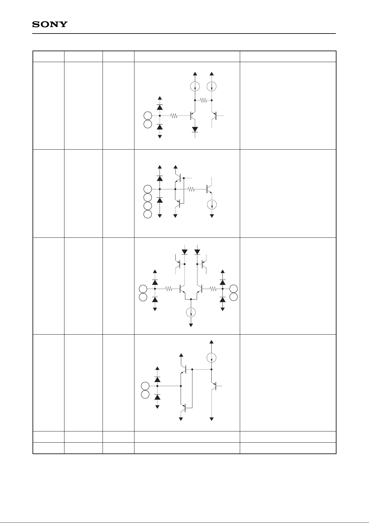
Pin Description
Pin No.
1
2
3
4
5
6
13
Symbol
VCC
SW1
IN1
OUT1 a
OUT1 b
IN2 X
IN4 X
Pin voltage
5V
0V
0V
0V
Equivalent circuit
Description
Positive supply voltage pin.
Control pin of switch unit.
The signal input from IN1 is
selected for "a" side or "b" side
by the SW1 applied voltage.
When SW1 is 2V or less, low
turns to "a" side; it is 2.6V or
more, high turns to "b" side.
Input pin of switch unit.
Output pins of switch unit.
The pin which is not selected is
GND.
Multiplier IN X input pins.
2
500
50µA
2.3V
500
50µA
3
100µA
4
5
2mA
500
100µA
6
13
100µA
Page 3
– 3 –
CXA1726AM/AS
Pin No.
15
7
14
9
24
10
23
11
22
Symbol
GND
IN2 Y
IN4 Y
IN3–
IN6–
IN3+
IN6+
OUT3
OUT6
Pin voltage
0V
0V
0V
Equivalent circuit
Description
GND
Multiplier IN Y input pins.
8
12
21
25
OUT2
OUT4
OUT7
OUT5
0V
0V
0V
0V
Multiplier output pins.
Operational amplifier input pins.
Operational amplifier output pins.
16
VEE
–5V
Negative supply voltage pin.
500
100µA
100µA
7
14
12
21
25
56k
8
50µA
1k
50µA
9
23
24
10
22
100µA
11
Page 4

– 4 –
CXA1726AM/AS
18
20
27
29
17
19
26
28
IN7 Ya
IN7 Xa
IN5 Ya
IN5 Xa
IN7 Yb
IN7 Xb
IN5 Yb
IN5 Xb
0V
Input pins of multiplier with
switch.
30
SW2
Switch pin to select "a" side or
"b" side of multiplier with switch.
"a" side ≤ 2.0V
"b" side ≥ 2.6V
17
19
20
26
27
28
29
500
50µA
18
500
50µA
50µA
50µA
50µA
30
No.
Item
Symbol
Conditions
Measurement
point
Min.
Typ.
Max.
Unit
1
2
3
4
5
6
7
Output offset voltage
Scale factor
Frequency response
Input dynamic range
Output dynamic range
Input bias current
Delay time
VO
SF
GT
VIN
VOUT
IIB
DT
X = Y = 0V
X = Y = 1V → V1
X = –Y = 1V → V2
(| V1 | + | V2 |)/2 = SF
X = 1V, Y = SG1
X = Y = 1V
X = 1V, Y = SG2
OUT
X, Y
Y, OUT
–110
0.95
–3
–3
50
16
1
–0.5
125
110
1.05
1
±2.3
±2.7
3
200
mV
—
dB
V
V
µA
ns
Input
t
Output
100%
50%
0%
Measure "t".
Electrical Characteristics
Multiplier
Pin No.
Symbol
Pin voltage
Equivalent circuit
Description
Page 5

– 5 –
CXA1726AM/AS
20
21
Current consumption 1
Current consumption 2
ICC
IEE
A1
A16
21
–33
26
–26
33
–21
mA
mA
13
14
15
16
17
18
19
Frequency response
Switch threshold high
Switch threshold low
Output dynamic range
Input bias current
Output offset voltage
Delay time
GT
VSH
VSL
VOUT
IIB
VO
DT
IN = SG1
IN = 0V
IN = 0V
X = 1V, Y = SG2
OUT
SW
SW
OUT
IN
OUT
IN, OUT
–3
2.5
–1
–15
50
–0.15
–0.4
–3
113
1
2.0
±3.1
1
15
200
dB
V
V
V
µA
mV
ns
Input
t
Output
100%
50%
0%
Measure "t".
Switch
8
9
10
11
12
Input bias current
Voltage gain
Output dynamic range
Frequency response
Input offset voltage
IIB
AV
VOUT
GT
VI
IN = 0V
Inversed input pin = SG1
Non-inversed input pin = GND
IN = 0V
IN
OUT
–1
50
–3
–6
0.35
80
–0.15
–2
1
±3.65
1.4
+6
µA
dB
V
dB
mV
Operational Amplifier
No.
Item
Symbol
Conditions
Measurement
point
Min.
Typ.
Max.
Unit
No.
Item
Symbol
Conditions
Measurement
point
Min.
Typ.
Max.
Unit
No.
Item
Symbol
Conditions
Measurement
point
Min.
Typ.
Max.
Unit
Page 6

– 6 –
CXA1726AM/AS
Electrical Characteristics Measurement Circuit
10k
1V
VCC
SW1
IN1
OUT1a
OUT1b
IN2X
IN2Y
OUT2
IN3–
IN3+
OUT3
OUT4
IN4X
IN4Y
GND
SW2
IN5Xa
IN5Xb
IN5Ya
IN5Yb
OUT5
IN6–
IN6+
OUT6
OUT7
IN7Xa
IN7Xb
IN7Ya
IN7Yb
V
EE
16
17
18
19
20
21
25
26
27
28
29
30
2
3
4
5
6
7
8
9
10
11
12
13
14
15
1
mul.
mul.
L
H
H
L
mul.
L
H
L
H
mul.
L
H
L
H
1V
SG2
S27B
S27C
SG2
S26B
S26C
3.9k
22
23
24
1k
S24
SG1
10k 10µ
10k
5p
1V
S20
1V
S19
SG2
S18B
S18C
1V 1V
1V 1V
1V 1V
SG2
S17B
S17C
1V 1V
1V
S13
S14A
SG2
S14B
S14C
1V1V
3.9k
1k
S9
SG1
10k
10µ
10k
5p
S7A
SG2
S7B
S7C
1V1V
3.9k
1V
S6
3.9k
3.9k
S3
S2
SG1
10k
5V
A1
A1G
3.9k
S30
S29
S28
S27A
S26A
S18A
S17A
5V
Page 7

– 7 –
CXA1726AM/AS
Application Circuit
GND
IN4 Y
IN4 X
OUT4
OUT3
IN3+
IN3–
OUT2
IN2 Y
IN2 X
OUT1b
OUT1a
IN1
SW1
V
CC
V
EE
IN7 Yb
IN7 Ya
IN7 Xb
IN7 Xa
OUT7
OUT6
IN6+
IN6–
OUT5
IN5 Yb
IN5 Ya
IN5 Xb
IN5 Xa
SW2
GND
C2
0.001µ
R2
10k
R4
5.6k
GND
R1
22k
GND GND
R3
3.3k
C1
22µ
V.SIN
GNDGND GND
GND
C5
5p
R5
10k
R6
5.6k
R9
33k
R8
5.6k
GND
C3
22µV15V
C4
22µ
V2
5V
GND
GND
R7
5.6k
16
17
18
19
20
21
22
23
24
25
26
27
28
29
30
2
3
4
5
6
7
8
9
10
11
12
13
1415
1
V4
VSIN
VPARA–
VPARA+
VSAW–
VSAW+
VGEN
VAGC
VGND
VDIN
VSQ
HSQ
HDIN
V
CC
VCLP
HCLP
HPARA–
HPARA+
HSAW–
HSAW+
HAGC
HGND
HDLY
HBIAS
VREF
VBIAS
IREF
V
EE
GND GND
C7
47µV35V
GNDGND
HDINVDIN
C6
0.047µ
GNDGND
C11
0.1µ
GND
R18
51k
GND GND
C12
47µ
V4
5V
R13
8.2k
GND
R11
2.2k
GND
GND
R12
1.5k
GND
R14
1k
GND
C10
1µ
GND
C8
1µ
GND
C9
0.047µ
A1726AM/AS
A1470AM/AS
2
3
4
5
6
7
8
9
10
11
12
13
14
1
0.1µ
16
17
18
19
20
21
22
23
24
25
26
27
2815
2
Application circuits shown are typical examples illustrating the operation of the devices. Sony cannot assume responsibility for
any problems arising out of the use of these circuits or for any infringement of third party patent and other right due to same.
Page 8

– 8 –
CXA1726AM/AS
Input Signals
Description of Operation
• Multiplier
The input X and Y signals of the multiplier are multiplied and output to the OUT pins.
• Operational amplifier
This inputs the signals which have been output from the multiplier.
∗
Care is required with ringing in the operational amplifier. Placing a 5p capacitor in parallel with the feedback
resistor is recommended as a preventive measure.
• Switch
The signal input from IN1 is selected for "a" side or "b" side by the SW1 applied voltage.
When SW1 is 2V or less, low turns to "a" side; it is 2.6V or more, high turns to "b" side.
The unselected output pin is connected to GND.
∗
For the multipliers with a switch, "a" side or "b" side is selected under the same conditions.
f = 200kHz
3Vp-p
GND
GND
5Vp-p
f = 1MHz
SG1
SG2
Page 9

– 9 –
CXA1726AM/AS
[dB]
0
–4
–8
–12
–14
10k 100k 1M 10M [Hz]
Multiplier frequency response
X
Y
mul.
OUT
Input X = DC 1V
Y = 5Vp-p Sine wave
[dB]
0
–4
–8
–12
10k 100k 1M 10M
Operational amplifier frequency response
OUT
Input 5Vp-p Sine wave
IN
10k
10k
[Hz]
2
1
0
–1
–2
–2 –1 1 2
OUT
[V]
Y [V]
Multiplier gain characteristics
Input X = 1V
Y = –2 to +2V
Page 10

– 10 –
CXA1726AM/AS
Package Outline Unit: mm
CXA1726AM
CXA1726AS
0.45 ± 0.1
1
1.27
15
7.6 – 0.1
+ 0.3
10.3 ± 0.4
16
30
18.8 – 0.1
+ 0.4
0.2
M
0.1
0.2 – 0.05
+ 0.1
0.5 ± 0.2
0.1 – 0.05
A
(9.3)
2.3 – 0.15
+ 0.4
30PIN SOP(PLASTIC)
SONY CODE
EIAJ CODE
JEDEC CODE
SOP-30P-L03
SOP030-P-0375
PACKAGE MATERIAL
LEAD TREATMENT
LEAD MATERIAL
PACKAGE MASS
EPOXY RESIN
SOLDER PLATING
COPPER ALLOY
PACKAGE STRUCTURE
0.7g
0° to 10°
+ 0.2
DETAIL A
SONY CODE
EIAJ CODE
JEDEC CODE
30PIN SDIP (PLASTIC)
26.9 – 0.1
+ 0.4
15
16
30
1.778
10.16
8.5 – 0.1
+ 0.3
0.25 – 0.05
+ 0.1
0° to 15°
0.5 ± 0.1
0.9 ± 0.15
3.0 MIN
0.5 MIN
3.7 – 0.1
+ 0.4
SDIP-30P-01
SDIP030-P-0400
1
PACKAGE STRUCTURE
MOLDING COMPOUND
LEAD TREATMENT
LEAD MATERIAL
PACKAGE MASS
EPOXY RESIN
PLATING
COPPER ALLOY
1.8g
SOLDER/PALLADIUM
1.All mat surface type.
Two kinds of package surface:
2.All mirror surface type.
NOTE : PALLADIUM PLATING
This product uses S-PdPPF (Sony Spec.-Palladium Pre-Plated Lead Frame).
 Loading...