

Page 1
—1—
E92121B79-TE
Sony reserves the right to change products and specifications without prior notice. This information does not convey any license by
any implication or otherwise under any patents or other right. Application circuits shown, if any, are typical examples illustrating the
operation of the devices. Sony cannot assume responsibility for any problems arising out of the use of these circuits.
Structure
Bipolar silicon monolithic IC
Absolute Maximum Ratings (Ta=25 °C)
• Supply voltage VCC 8V
•Operating temperature Topr –10 to +60 °C
• Storage temperature Tstg –65 to +150 °C
• Allowable power dissipation
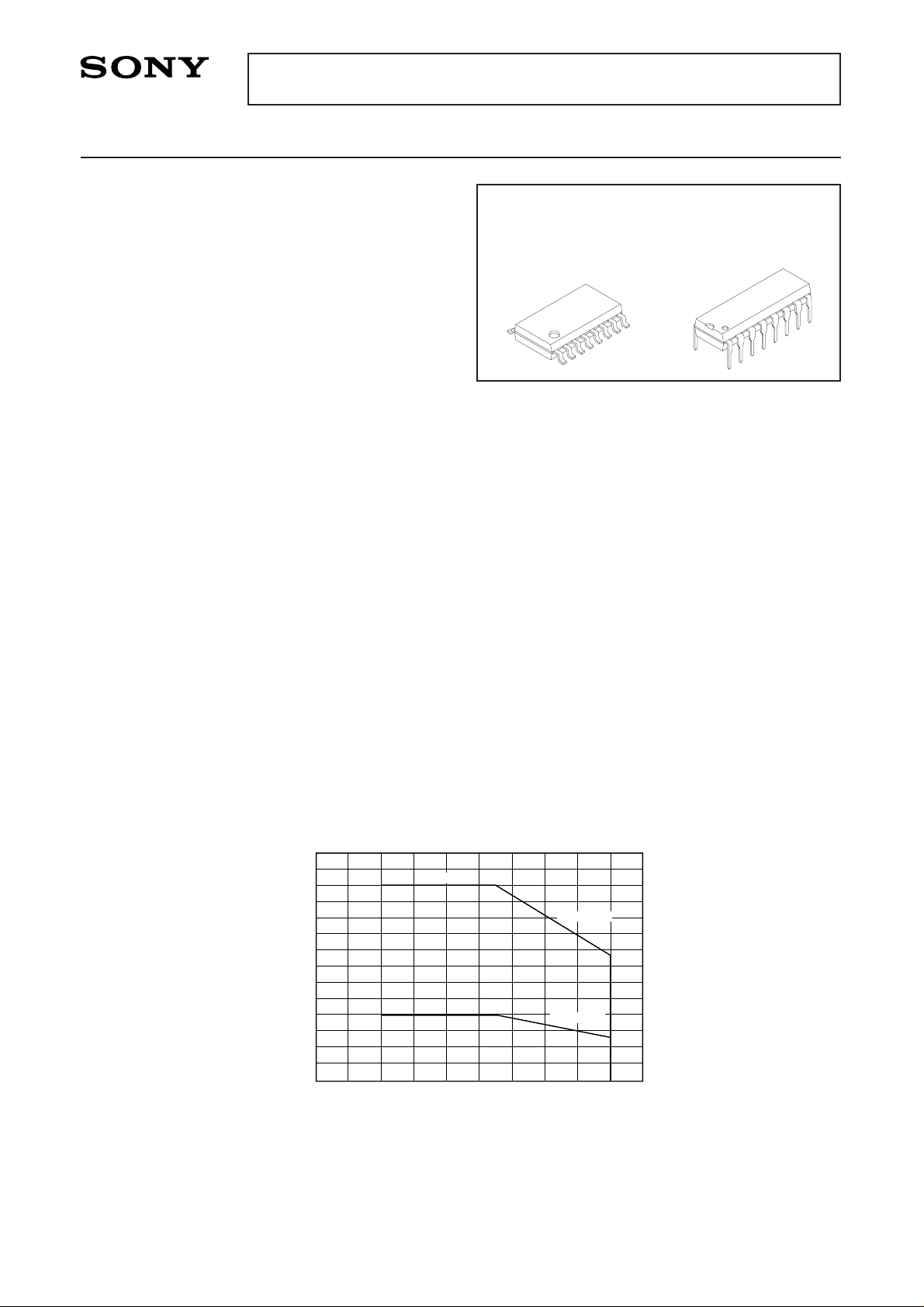
PD 410 (CXA1622M) mW
1200 (CXA1622P) mW
Operating Conditions (Ta=25 °C)
• Supply voltage
• Stereo mode
{
1.8 V to 4.5 V (CXA1622M)
1.8 V to 7.0 V (CXA1622P)
• Monaural BTL mode 1.8 V to 4.5 V
(3 V recommended)
Description
The CXA1622M/P is a bipolar IC developed as
power amplifier for compact radio cassettes with
built-in pre-amplifier and power amplifier electrical
volume.
Features
• Use one channel in stereo mode
· EIAJ output=110 mW (Typ.), VCC=3 V, RL=8 Ω
(CXA1622M)
· EIAJ output=450 mW (Typ.), VCC=6 V, RL=8 Ω
(CXA1622P)
• BTL mode
· EIAJ output=320 mW (Typ.), VCC=3 V, RL=8 Ω
(CXA1622M)
· EIAJ output=360 mW (Typ.), VCC=3 V, RL=8 Ω
(CXA1622P)
• Built-in electrical volume
• Built-in ripple filter (ripple rejection 34.5 dB typ.)
• Selection between stereo power amplifier and
monaural BTL power amplifier is possible by
switching Pin 2.
Applications
Suitable for audio power amplifier for stereo and
monaural radios and power amplifier for radio
cassette and Walkman.
Stereo Power Amplifier/Monaural BTL Power Amplifier
CXA1622M CXA1622P
16 pin SOP (Plastic) 16 pin DIP (Plastic)
1000
500
PD-Power dissipation (mW)
Power dissipation curve
Free air
CXA1622P
CXA1622M
–30 –20 –10 0 10 20 30 40 50 60 70
Ta-Ambient temperature (°C)
CXA1622M/P
Page 2
—2—
CXA1622M/P
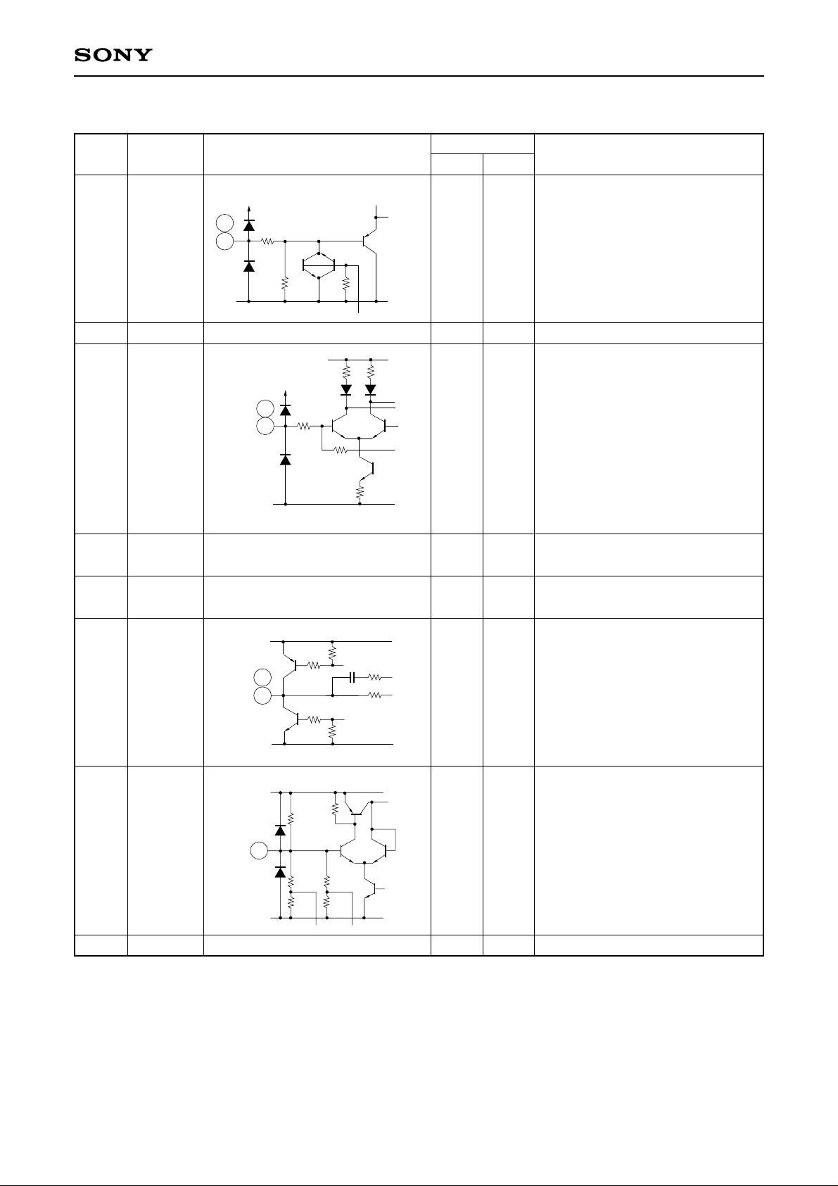
Pin Description
Pin
Symbol Equivalent circuit
Pin voltage
Description
No. 3 V 6 V
1, 16
3
4, 13
5, 12
6, 11
7, 10
8
9
IN1
IN2
NC
NF1
NF2
GND1
GND2
P-GND1
P-GND2
OUT1
OUT2
RIPPLE
VCC
VCC
11k
7.5k
GND
16
1
4.7k
100k
GND
VCC
13
4
GND
V
CC
100k
10
7
VCC
8.5k
73k 73k
90k 90k
8
0
—
1.5
0
0
1.5
2.72
3
0
—
3
0
0
3
5.43
6
Input
Power amplifier NF.
Connected to time constant 4.7 µF.
Pre-amplifier GND
Power amplifier GND
Power amplifier output
Connected to time constant 10 µF
for ripple filter.
VCC
Page 3
—3—
CXA1622M/P
Pin
Symbol Equivalent circuit
Pin voltage
Description
No. 3 V 6 V
14
15
2
VOL
REG
SW
VCC
20k
80k
GND
14
VCC
4k
24k
15
VCC
15k
15k
REG
2
0 to
1.25
1.25
1.25
0 to
1.25
1.25
1.25
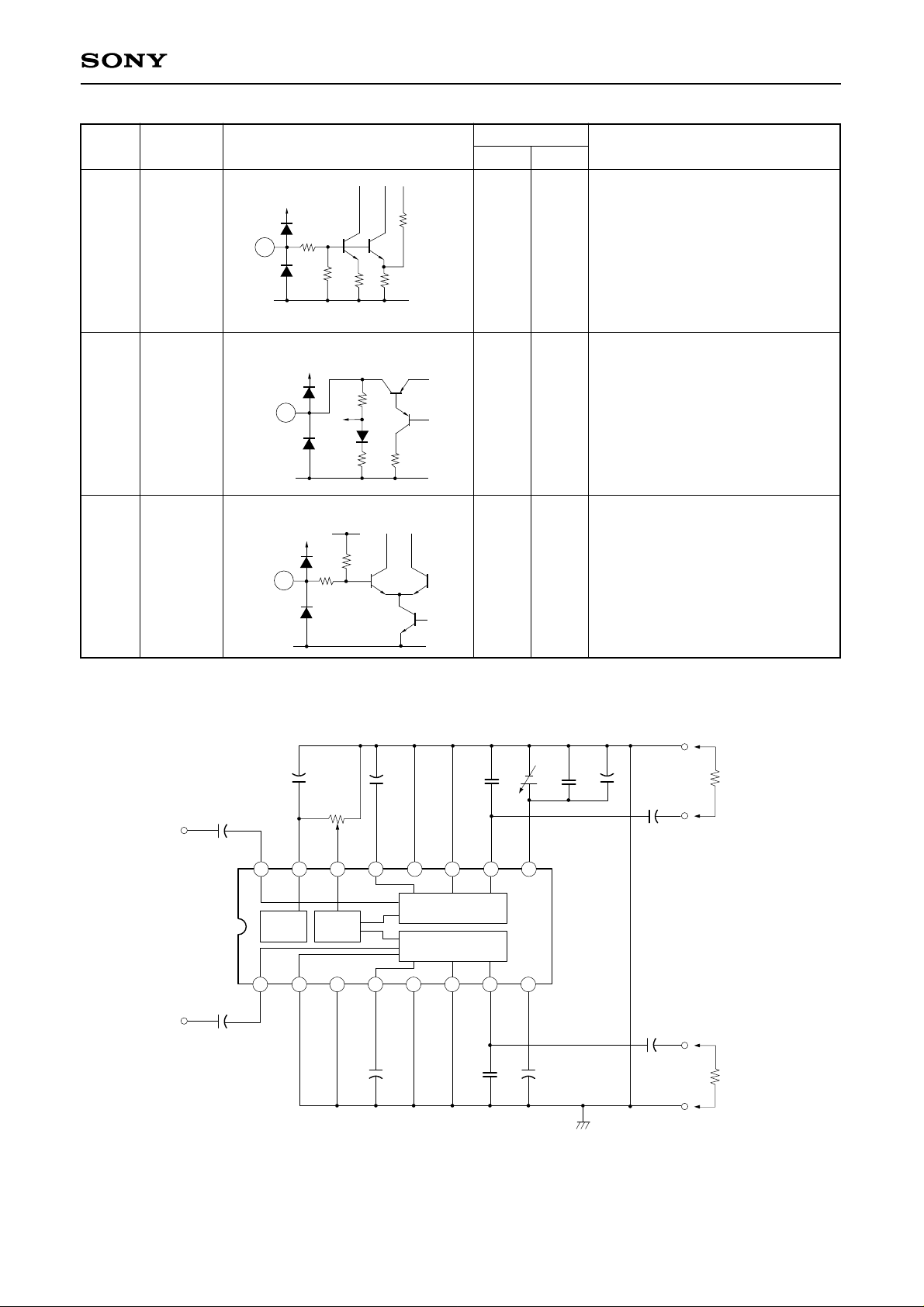
Control gain with change in voltage
(0 to 1.25 V) to electrical volume
control pin.
Regulator pin
Mode selection SW
• BTL mode when open
• Stereo mode when connected to
GND
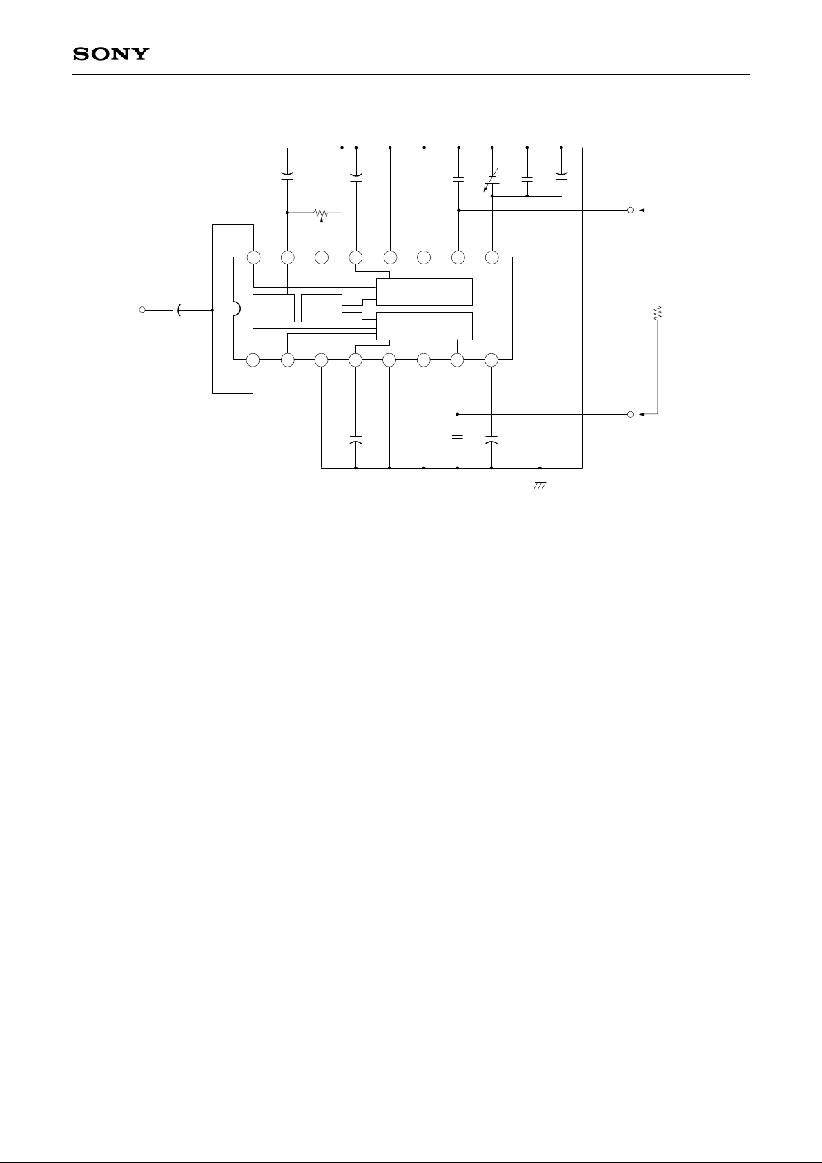
Block Diagram, Pin Configuration, and Application Circuit
1) Stereo mode
+
+
+
+
+ +
+
+
+
IN1
C2
10µ
C3
10µ
IN1IN2
REGSW
VOLNC
NF1NF2
GNDGND
P GND1P GND2
OUT1OUT2
V
CCRIPPLE
R1
50k
C5
3.3µ
C7
0.1µ
C9
0.1µ
C10
220µ
C12
220µ
V1
3V
GND
SP1
8
OUT1
16 15 14 13 12 11 10 9
87654321
REG VOL
PRE+POWER1
PRE+POWER2
IN2
C1
10µ
C4
3.3µ
C5
0.1µ
C8
10µ
C11
220µ
GND
GND
OUT2
SP2
8
Page 4
—4—
CXA1622M/P
2) BTL mode
+
+
+
+ +
+
IN
C1
C2
10µ
IN1IN2
REGSW
VOLNC
NF1NF2
GNDGND
P GND1P GND2
OUT1OUT2
V
CCRIPPLE
R1
50k
C4
3.3µ
C6
0.1µ
C8
0.1µC9220µ
V1
3V
SP2
8
OUT+
16 15 14 13 12 11 10 9
87654321
REG VOL
PRE+POWER1
PRE+POWER2
C3
3.3µ
C5
0.1µ
C7
10µ
GND
OUT–
10µ
∗ The input signal enters the pre-amplifier with attenuation controlled with DC at Pin 14 and then it is amplified
by the approximately 30 dB (fixed) power amplifier.
∗ The state of Pin 2 can be used to select between stereo mode and monaural BTL mode.
The pre-power 1 and pre-power 2 output are positive phase output when Pin 2 is GND. Pre-power 2 is
inverse output of pre-power 1 output when Pin 2 is open.
Application circuits shown are typical examples illustrating the operation of the devices. Sony cannot assume responsibility for
any problems arising out of the use of these circuits or for any infringement of third party patent and other right due to same.
Page 5

—5—
CXA1622M/P
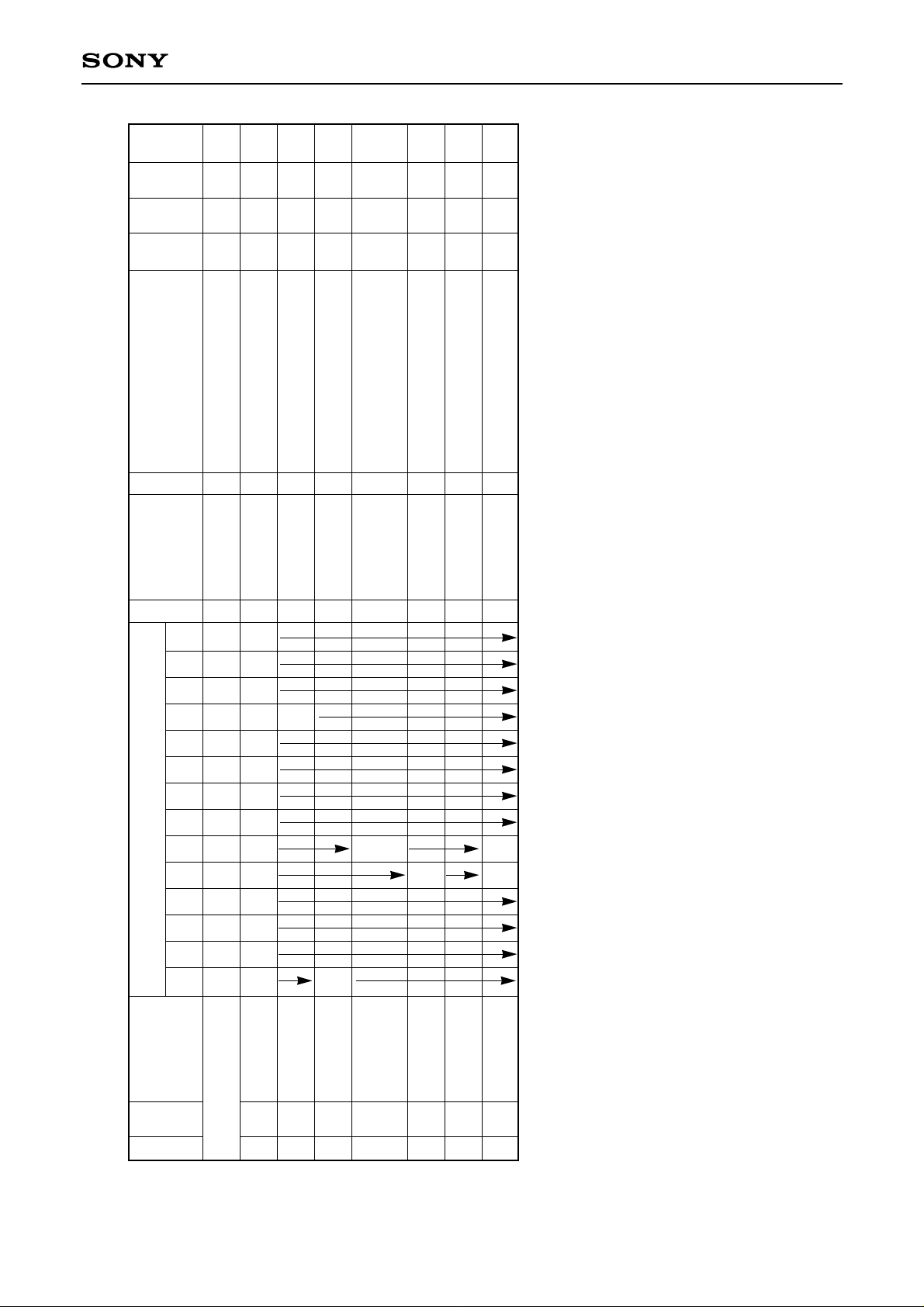
Test
No.
Test item
Circuit current
during no signal
Audio voltage
gain Lch
Audio voltage
gain Rch
Channel balance
Attenuation Lch
Attenuation Rch
EIAJ output Lch
EIAJ output Rch
Audio distortion
factor Lch
Audio distortion
factor Rch
Residual noise
level Lch
Residual noise
level Rch
Crosstalk L → R
Crosstalk R → L
BIAS SW conditions
S
1 S2 S3 S4 S5 S6 S7 S8 S9 S10 S11 S12 S13 S14
OFF OFF OFF ON OFF OFF ON OFF OFF OFF OFF OFF OFF OFF
ON ON OFF ON
OFF ON OFF ON
ON OFF ON ON OFF
OFF ON OFF ON
ON OFF ON ON OFF
OFF ON OFF ON
ON OFF ON OFF
OFF ON OFF ON
OFF OFF OFF OFF OFF ON OFF
OFF ON
ON ON
OFF ON ON OFF
Input waveform and
bias description
Output waveform and
description of test method
Circuit current during no signal
V
1=–40 dBm 1 kHz
V
1=–40 dBm 1 kHz
L and R channel balance
V1=–40 dBm 1 kHz
Output level difference between
max volume and half volume
V
1=–40 dBm 1 kHz
Output level difference between
max volume and half volume
V
1=–20 dBm 1 kHz, RL=8 Ω
Output level where THD=10 %
V
1=–20 dBm 1 kHz, RL=8 Ω
Output level where THD=10 %
V
1=–20 dBm 1 kHz, RL=8 Ω
Distortion factor when output is 50 mW
V
1=–20 dBm 1 kHz, RL=8 Ω
Distortion factor when output is 50 mW
Noise level during no signal at
max volume
Noise level during no signal at
max volume
V
1=–40 dBm 1 kHz
Rch output level when Lch is input
V
1=–40 dBm 1 kHz
Lch output level when Rch is input
Function block
Input point
Test point
Typical conditions for each bias
Min. Typ. Max. Unit
1.0 3.0 8.2mA1.0 3.0 7.7
28 33.7 38dB27 32.6 36
28 33.7 38dB27 32.6 36
–3 0 3 dB
1.5 5.8 12
dB
1.0 4.3 12
1.5 5.8 12
dB
1.0 4.3 12
350 450
mW
90 110
350 450
mW
90 110
0.7 2.5 %
0.7 2.5 %
–65 –60 dBm
–65 –60 dBm
–60 –56 dBm
–60 –56 dBm
I1
V4
V5
V4
V5
V4
V5
V4
V5
V4
V5
V4
V5
1
2
3
4
5
6
7
8
9
10
11
12
13
14
Stereo mode
Upper : CXA1622M (VCC=3 V)
Lower : CXA1622P (VCC=6 V)
{
Page 6
—6—
CXA1622M/P
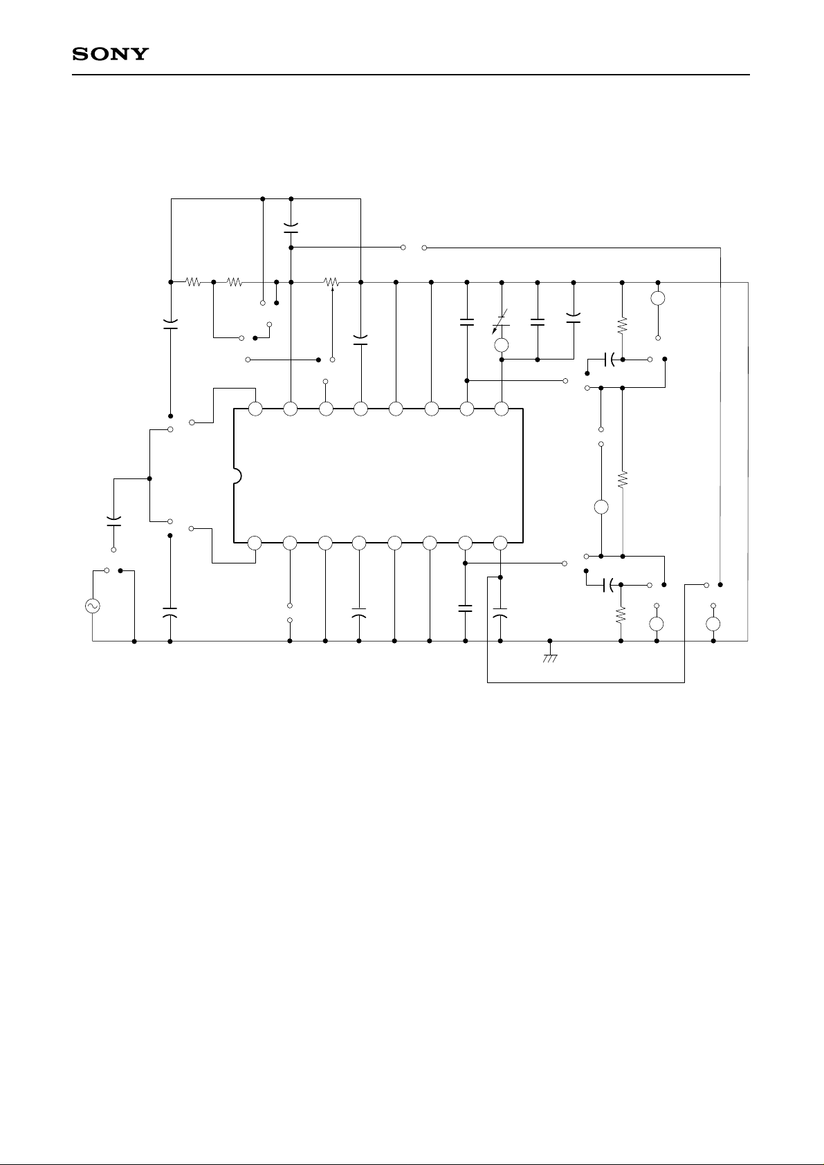
Test
No.
Test item
Circuit current
during no signal
Output
DC bias lag
Audio voltage gain
Attenuation
EIAJ output
Audio distortion
factor
Residual noise level
BIAS SW conditions
S
1 S2 S3 S4 S5 S6 S7 S8 S9 S10 S11 S12 S13 S14
OFF ON ON OFF OFF OFF ON OFF ON ON OFF ON ON OFF
ON
ON
ON
ON
OFF OFF
Input waveform and
bias description
Output waveform and
description of test method
Circuit current during no signal
Output DC bias lag
V
1=–40 dBm 1 kHz
V
1=–40 dBm 1 kHz
Output level difference between
max volume and half volume
V
1=–20 dBm 1 kHz, RL=8 Ω
Output level where THD=10 %
V
1=–20 dBm 1 kHz, RL=8 Ω
Distortion factor when output is 50 mW
Noise level during no signal at
max volume
Function block
Input point
Test point
Typical conditions for each bias
Min. Typ. Max. Unit
3 7 mA
0 30 mV
34 38 42dB30 37 43
1.5 6.0 12dB1.0 5.0 12
260 360
mW
220 320
2.5 %
–65 –62 dBm
I1
|V3|
V
3
V3
V3
V3
V3
1
2
3
4
5
6
7
BTL mode VCC=3 V
Upper : CXA1622M
Lower : CXA1622P
Page 7
—7—
CXA1622M/P
Electrical Characteristics Test Circuit
16 15 14 13 12 11 10 9
87654321
+
+
+
+
+
+
+
+
+
+
GND
+
A
V
Y
V V
C3
10µ
C4
10µ
C6
3.3µ
C8
0.1µ
C10
0.1µ
C11
220µ
C13
220µ
C12
220µ
C9
10µ
C7
0.1µ
C5
3.3µ
R1
25kR225k
R3
50k
S7
S8
S9
S12
S11
S14
S13
S18
S6
S5
S2
S1
S3
S4
C1
10µ
C2
10µ
V1
RC
V2
3V V4
V6V5
I1
R6
8
R4
8
R5
8
Y3
IN1IN2
VOLNC
NF1NF2
GNDGND
OUT1OUT2
V
CC
RIPPLE
P GND1P GND2
REGSW
CXA1622M/P
Notes on Operation
• Set print pattern to low impedance because Pins 6 and 11 are GND of power amplifier output stage.
• The value of the phase correction capacitance attached to Pins 7 and 10 varies slightly according to the
print pattern.
• Provide a large land for DIP type Pin 5 because it also serves as heat dissipation pin.
• Place the by-pass capacitor of VCC (Pin 9) as close to the pin as possible.
Page 8

—8—
CXA1622M/P
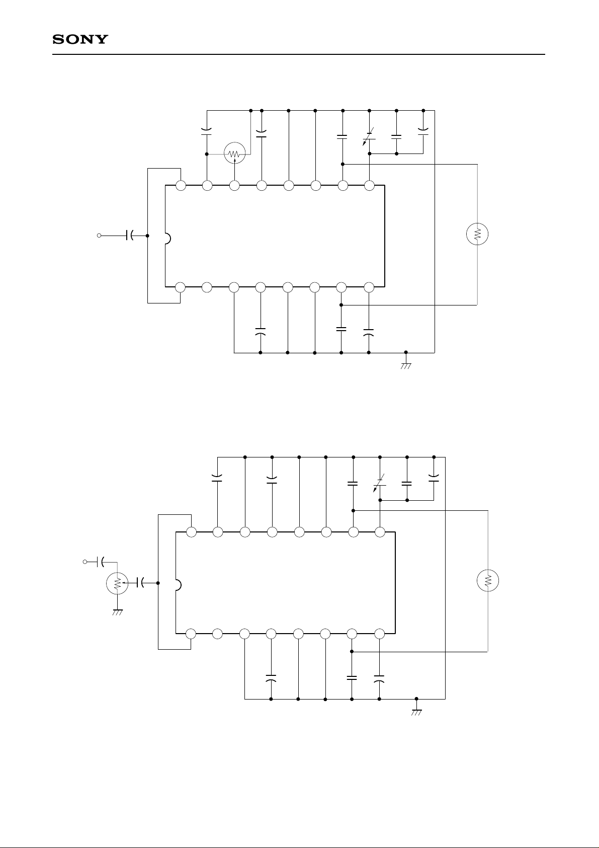
Stereo output single mode
Monaural output BTL mode
16 15 14 13 12 11 10
854321
+
+
+
++
+
+
+
+
GND
C2
10µ
C3
10µ
C5
3.3µ
C7
0.1µ
C9
0.1µ
C10
220µ
C12
220µ
C11
220µ
C8
10µ
C5
0.1µ
C4
3.3µ
R1
50k
C1
10µ
V1
3V
R3
8
IN1
IN1
IN2
IN2
VOL
NC
NF1
NF2
GND
GND
OUT1
OUT2
VCC
RIPPLE
P GND1
P GND2
REG
SW
CXA1622M/P
9
∗
∗
R2
8
6 7
Keep the by-pass capacitor close to the IC pins
16 15 14 13 12 11 10
854321
+
+
+
+
+
+
GND
C1
10µ
C2
10µ
C4
3.3µ
C5
0.1µ
C8
0.1µ
C9
220µ
C7
10µ
C5
0.1µ
C3
3.3µ
R1
50k
V1
3V
IN1
IN
IN2
VOL
NC
NF1
NF2
GND
GND
OUT1
OUT2
V
CC
RIPPLE
P GND1
P GND2
REG
SW
CXA1622M/P
9
∗
R2
8
6 7
∗
Keep the by-pass capacitor close to the IC pins
Page 9
—9—
CXA1622M/P
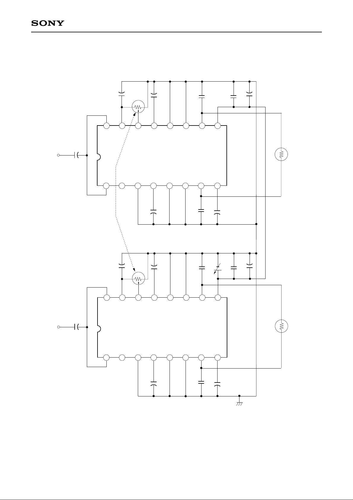
When using internal IC electrical volume in BTL mode
When using IC as fixed gain amplifier in BTL mode
Pin14 → GND (IC Gain MAX)
16 15 14 13 12 11 10
854321
+
+
+
+
+
+
GND
C2
10µ
C4
3.3µ
C5
0.1µ
C8
0.1µ
C9
220µ
C7
10µ
C5
0.1µ
C3
3.3µ
R1
50k
V1
3V
IN1
IN
IN2
VOL
NC
NF1
NF2
GND
GND
OUT1
OUT2
V
CC
RIPPLE
P GND1
P GND2
REG
SW
CXA1622M/P
9
R2
8
6 7
s.p
C1
10µ
16 15 14 13 12 11 10
854321
+
+
+
+
+
+
+
GND
C2
10µ
C4
3.3µ
C5
0.1µ
C8
0.1µ
C9
220µ
C7
10µ
C5
0.1µ
C3
3.3µ
V1
3V
IN1
IN
IN2
VOL
NC
NF1
NF2
GND
GND
OUT1
OUT2
V
CC
RIPPLE
P GND1
P GND2
REG
SW
CXA1622M/P
9
R2
8
6 7
s.p
C1
10µ
Page 10
—10—
CXA1622M/P
BTL, Stereo Application Circuit
When using internal IC electrical volume
16 15 14 13 12 11 10
854321
+
+
+
+
+
+
C1
10µ
C2
10µ
C4
3.3µ
C5
0.1µ
C8
0.1µ
C9
220µ
C7
10µ
C5
0.1µ
C3
3.3µ
R1
50k
IN1
IN
IN2
VOL
NC
NF1
NF2
GND
GND
OUT1
OUT2
V
CC
RIPPLE
P GND1
P GND2
REG
SW
CXA1622M/P
9
R2
8
6 7
s.p
Lch
16 15 14 13 12 11 10
854321
+
+
+
+
+
+
GND
C1
10µ
C2
10µ
C4
3.3µ
C5
0.1µ
C8
0.1µ
C9
220µ
C7
10µ
C5
0.1µ
C3
3.3µ
R1
50k
V1
3V
IN1
IN
IN2
VOL
NC
NF1
NF2
GND
GND
OUT1
OUT2
V
CC
RIPPLE
P GND1
P GND2
REG
SW
CXA1622M/P
9
R2
8
6 7
s.p
Rch
LINKAGE VOL.
Application circuits shown are typical examples illustrating the operation of the devices. Sony cannot assume responsibility for
any problems arising out of the use of these circuits or for any infringement of third party patent and other right due to same.
Page 11
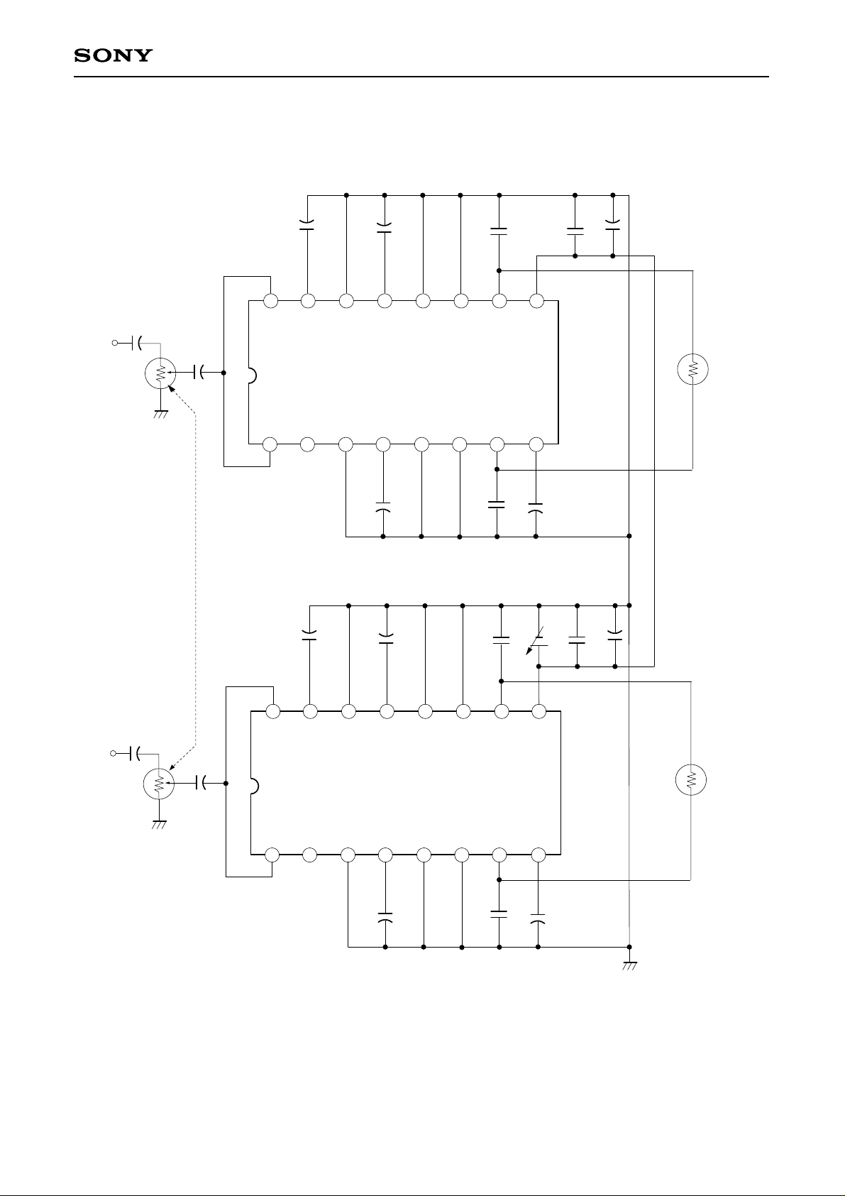
—11—
CXA1622M/P
BTL, Stereo Application Circuit
When using IC as fixed gain amplifier
Pin14 → GND (IC Gain Max)
16 15 14 13 12 11 10
854321
+
+
+
+
+
+
+
C1
10µ
C2
10µ
C4
3.3µ
C5
0.1µ
C8
0.1µ
C9
220µ
C7
10µ
C5
0.1µ
C3
3.3µ
IN1
IN
IN2
VOL
NC
NF1
NF2
GND
GND
OUT1
OUT2
V
CC
RIPPLE
P GND1
P GND2
REG
SW
CXA1622M/P
9
R2
8
6 7
s.p
Lch
16 15 14 13 12 11 10
854321
+
+
+
+
+
+
+
GND
C1
10µ
C2
10µ
C4
3.3µ
C5
0.1µ
C8
0.1µ
C9
220µ
C7
10µ
C5
0.1µ
C3
3.3µ
IN1
IN
IN2
VOL
NC
NF1
NF2
GND
GND
OUT1
OUT2
V
CC
RIPPLE
P GND1
P GND2
REG
SW
CXA1622M/P
9
R2
8
6 7
s.p
Rch
V1
3V
LINKAGE
Application circuits shown are typical examples illustrating the operation of the devices. Sony cannot assume responsibility for
any problems arising out of the use of these circuits or for any infringement of third party patent and other right due to same.
Page 12

—12—
CXA1622M/P
10
5
0
10 100 1000
VIN=–26dBm
f
IN=1kHz
R
L=8Ω
VCC=1.8V
VCC=3V
VCC=4.5V
IN=–26dBm
IN=–20dBm
10
5
0
10 100 1000
VIN=–26dBm
f
IN=1kHz
R
L=8Ω
VCC=1.8V
VCC=3V
10
5
0
10 100 1000
VIN=–26dBm
f
IN=1kHz
R
L=8Ω
VCC=1.8V
VCC=3V
VCC=4.5V
IN=–26dBm
IN=–20dBm
10
5
0
10 100 1000
VIN=–26dBm
f
IN=1kHz
R
L=8Ω
VCC=1.8V
VCC=3V
IN=–26dBm
IN=–20dBm
0
–10
–20
10 100 1k 10k 100k
output C=220µF
R
L=8Ω
IN=–40dBm,1kHz is
assumed as 0dB
0
–10
–20
10 100 1k 10k 100k
IN=–40dBm,1kHz is
assumed as 0dB
Output vs Distortion 1 CXA1622P
stereo mode single-channel input
Output vs Distortion factor 3
CXA1622P BTL mode
Output vs Distortion 2 CXA1622M
stereo mode single-channel input
Distortion factor [%]
Distortion factor [%]
Distortion factor [%] Distortion factor [%]
Output [mV] Output [mV]
Output [mV] Output [mV]
Output vs Distortion 4 CXA1622M BTL mode
Stereo mode frequency characteristics
V
IN=–40dBm VOL MAX VCC=3V
BTL mode frequency characteristics
VIN=–40dBm VOL MAX VCC=3V
Output [dB]
Output [dB]
Input signal frequency [Hz] Input signal frequency [Hz]
Page 13

Package Outline Unit : mm
CXA1622M/P
CXA1622M
16
1 8
0.45 ± 0.1
SONY CODE
EIAJ CODE
JEDEC CODE
16PIN SOP (PLASTIC)
+ 0.4
9.9 – 0.1
SOP-16P-L01
SOP016-P-0300
9
+ 0.3
5.3 – 0.1
7.9 ± 0.4
1.27
0.24
PACKAGE STRUCTURE
PACKAGE MATERIAL
LEAD TREATMENT
LEAD MATERIAL
PACKAGE MASS
+ 0.4
1.85 – 0.15
0.15
+ 0.2
0.1 – 0.05
6.9
+ 0.1
0.2 – 0.05
M
EPOXY RESIN
SOLDER PLATING
COPPER ALLOY
0.2g
0.5 ± 0.2
CXA1622P
+ 0.4
19.2 – 0.1
16
1 8
2.54
0.5 ± 0.1
1.2 ± 0.15
SONY CODE
EIAJ CODE
JEDEC CODE
DIP-16P-01
DIP016-P-0300
Similar to MO-001-AE
16PIN DIP (PLASTIC)
9
+ 0.4
0.5 MIN
3.7 – 0.1
3.0 MIN
+ 0.3
6.4 – 0.1
7.62
Two kinds of package surface:
1.All mat surface type.
2.All mirror surface type.
PACKAGE STRUCTURE
PACKAGE MATERIAL
LEAD TREATMENT
LEAD MATERIAL
PACKAGE MASS
EPOXY RESIN
SOLDER PLATING
COPPER ALLOY
1.0 g
+ 0.1
0.25 – 0.05
0° to 15°
—13—
 Loading...