

Page 1
—1—
E92311B8X
Sony reserves the right to change products and specifications without prior notice. This information does not convey any license by
any implication or otherwise under any patents or other right. Application circuits shown, if any, are typical examples illustrating the
operation of the devices. Sony cannot assume responsibility for any problems arising out of the use of these circuits.
Absolute Maximum Ratings (Ta=25 °C)
• Supply voltage VCC 7V
• Operating temperature Topr –20 to +75 °C
• Storage temperature Tstg –65 to +150 °C
Operating Conditions
Supply voltage VCC 1.8 to 4.5 V
Description
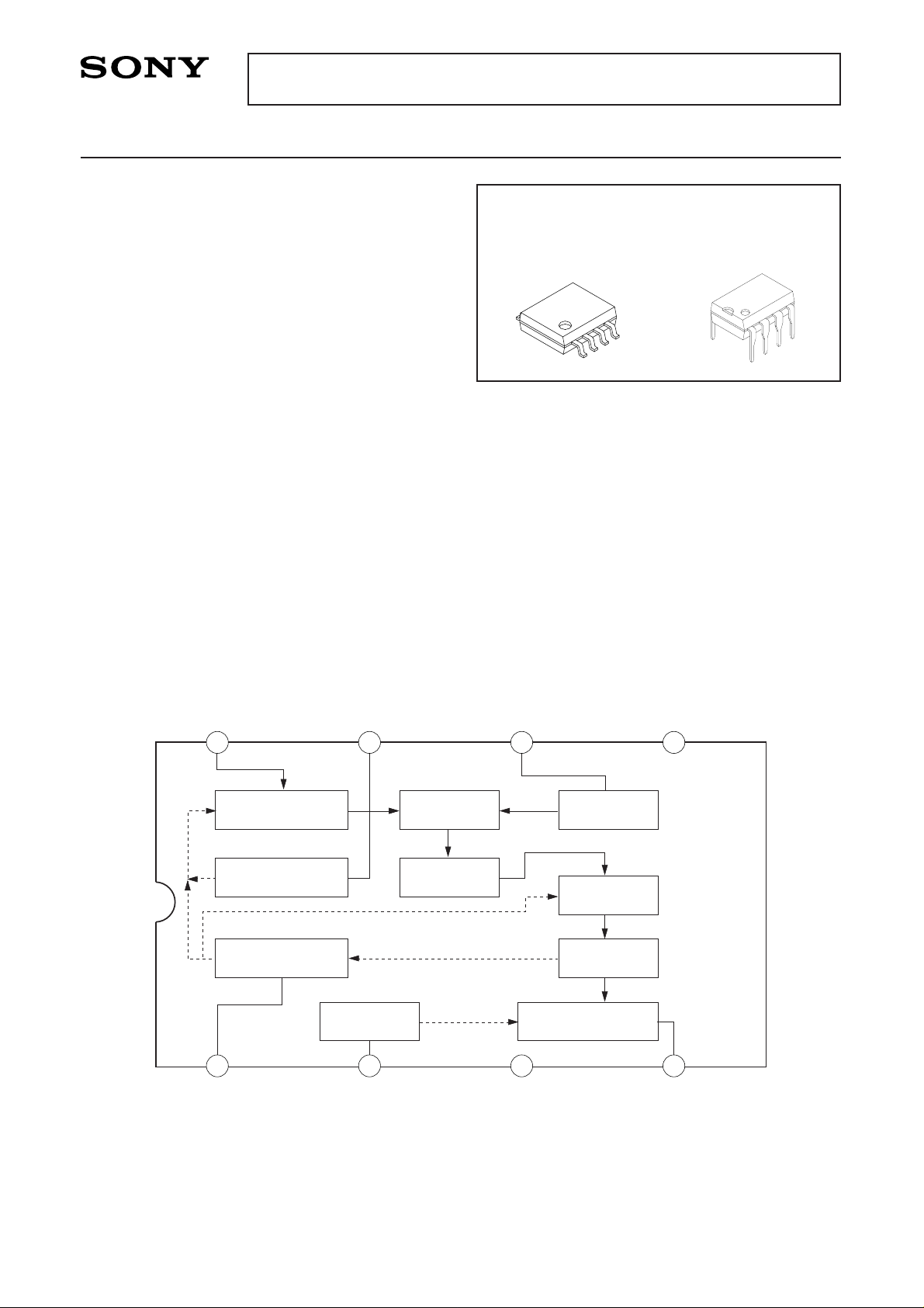
The CXA1600M/P is an 8-pin single-chip bipolar IC
for AM radios. This IC includes all functions from
the front-end to the power amplifier.
The CXA1600M/P doesn’t require any external
filter, making external ceramic filter attachment
unnecessary.
Features
• EIAJ output=100 mW (typ.)
(VCC=3 V, RL=8 Ω)
• Built-in electrical volume control.
• No ceramic filter required.
• Few peripheral components.
Applications
AM radio
Structure
Bipolar silicon monolithic IC
8-pin Single-chip AM Radio with Built-in Power Amplifier
CXA1600M CXA1600P
8 pin SOP (Plastic) 8 pin DIP (Plastic)
Block Diagram
RF AMP
OVERLOAD AGC
AGC
VOL
AF POWER AMP
IF DET
IF AMP
OSCMIXER
BPF
RF IN OL AGC LO OSC V
CC
AGC VOL GND SP OUT
1 2 3 4
5678
CXA1600M/P
For the availability of this product, please contact the sales office.
Page 2
—2—
CXA1600M/P
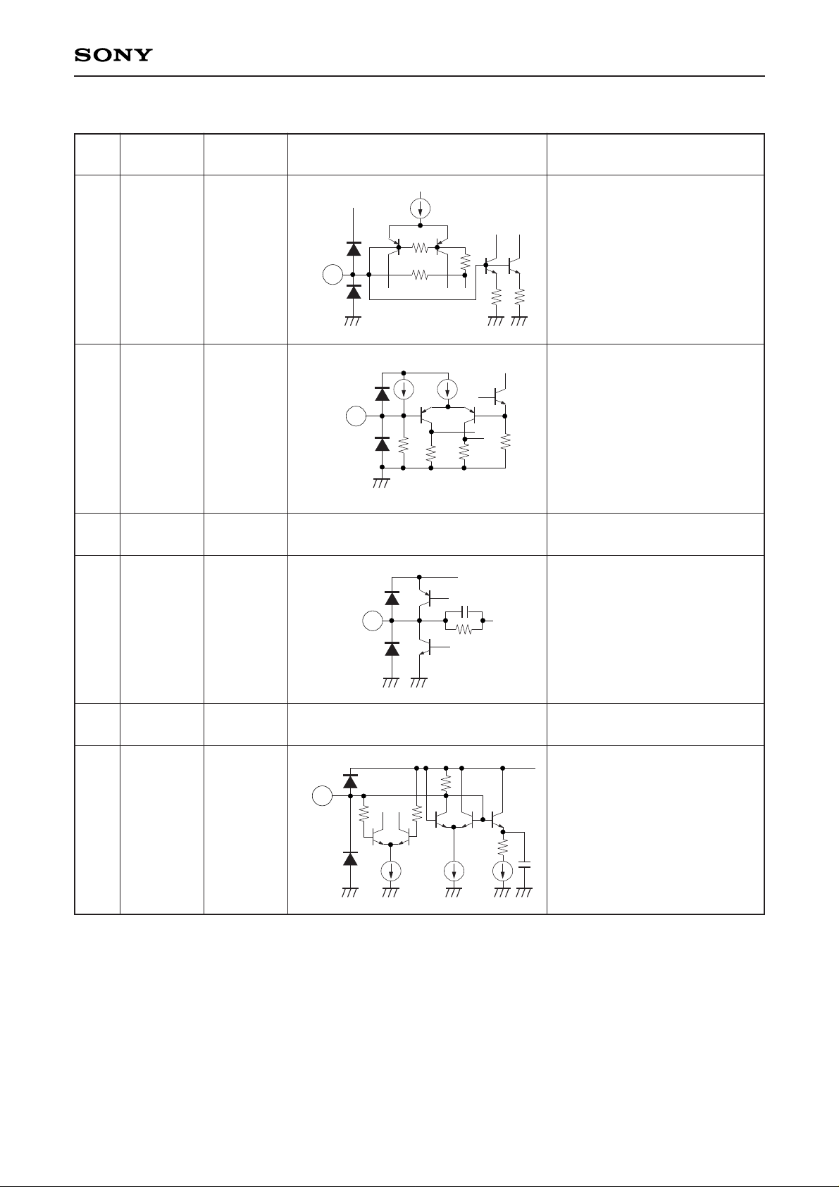
Pin Description VCC=3 V
No. Symbol
Voltage
Equivalent Circuit Description
(typ.)
1
2
3
4
5
6
AGC
VOL
GND
SP OUT
VCC
LO OSC
0.61 V
0.1 V
0 V
1.28 V
3 V
VCC
AGC
V
CC
GND
1
VCC
GND
VOL
2
VCC
GND
SP OUT
4
VCC
GND
LO OSC
6
Connect with a capacitor.
Connect to the midpoint of the
volume control.
Ground
Audio output.
Connect with a capacitor.
Power supply
Oscillation output.
Connect with an oscillation coil.
Page 3
—3—
CXA1600M/P
No. Symbol
Voltage
Equivalent Circuit Description
(typ.)
7
8
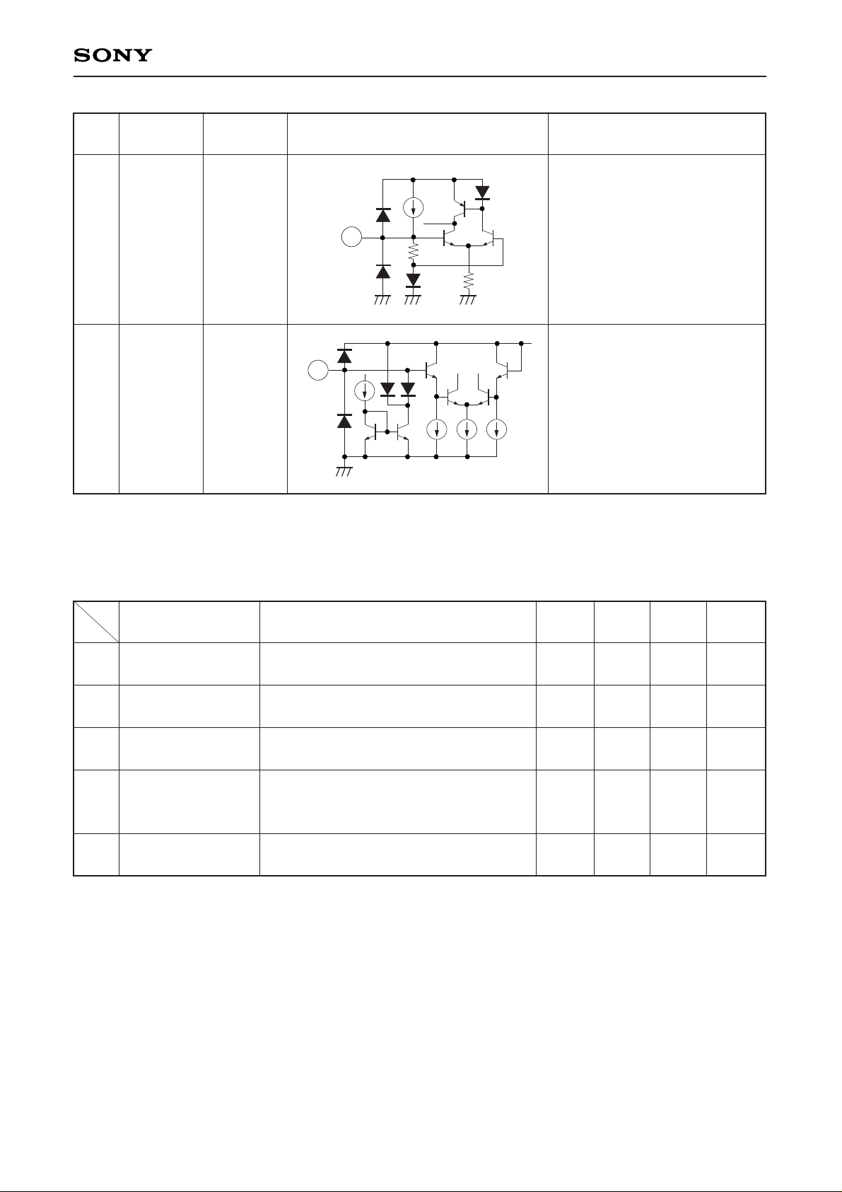
OL AGC
RF IN
0.62 V
3 V
VCC
GND
OL AGC
7
VCC
GND
RF IN
8
Connect with a capacitor.
RF input.
Connect with the antenna circuit.
Electrical Characteristics VCC=3 V, Ta=25 °C
1
2
3
4
5
Item
Non-signal
circuit current
EIAJ output
(with 8 Ω load)
Volume attenuation
Overall noise level
Selectivity
Test conditions
No signal
f=1 MHz, fMOD=1 kHz, 30 %
Vin=90 dBµV
f=1 MHz, fMOD=1 kHz, 30 %
Vin=90 dBµV, Volume=minimum
Short circuit at RF IN with a 1µF
capacitor. Measure the level at SP OUT.
Volume=maximum
f=1.010 MHz, fMOD=1 kHz, 30 %
Vin=35 dBµV.
Min. Typ. Max. Unit
4.8 6 10 mA
80 100 mW
–70 –65 dBm
–25 –15 dBm
14 19 dB
Page 4

—4—
CXA1600M/P
Noise
THD
AM I/O Characteristics
THD - Distortion factor [%]
Output level [dB]
Bar antenna input level [dBµV/m]
20 30 40 50 60 70 80 90 100 110 120
0
–10
–20
–30
–40
–50
–60
8
7
6
5
4
3
2
1
0
Output level [dB]
0
–10
–20
–30
–40
–50
–60
Selectivity Characteristics
–110 –100 –90 –80 –70 –60 –50 –40 –30 –20 –10 0 10 20 30
Input frequency (f
IN-fO) [kHz]
0dB=–10dBV
S+N
VCC=3V
f=1MHz
fMOD=1kHz
MOD=30%
Page 5
—5—
CXA1600M/P
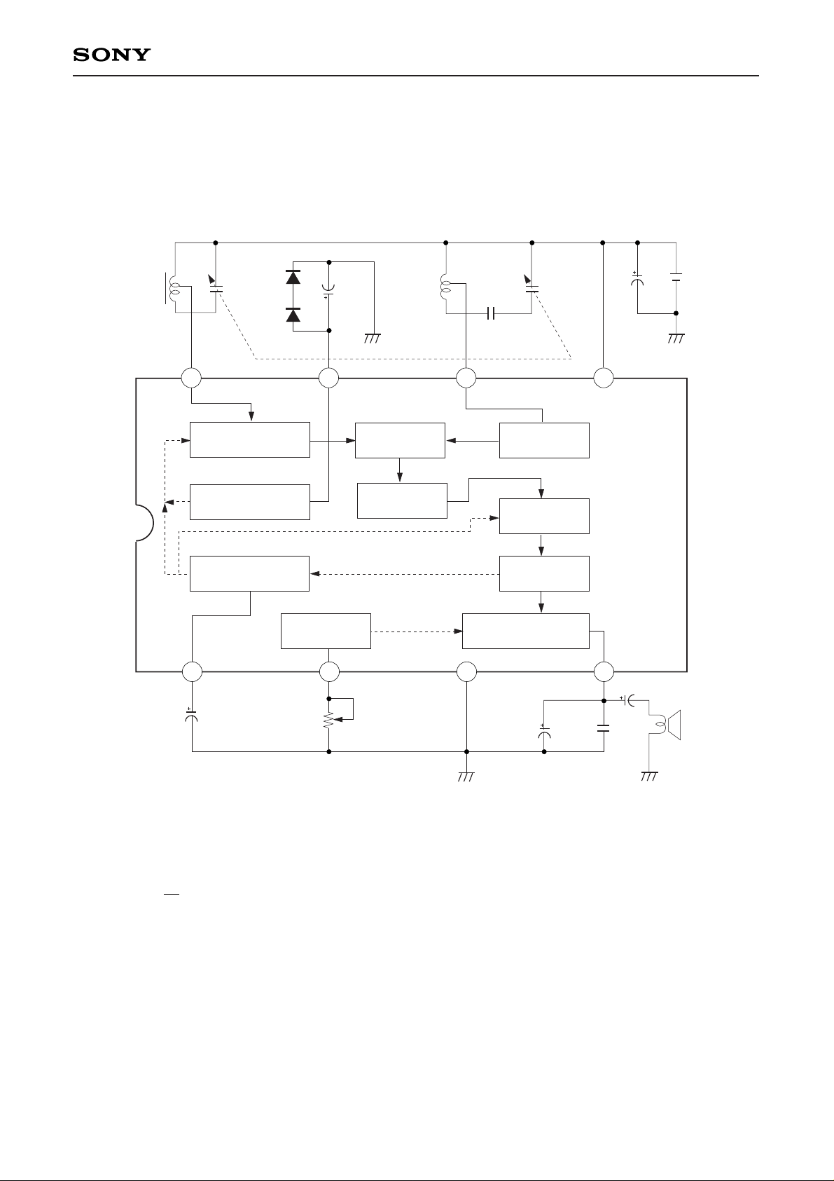
Notes on Applications
Application 1
The CXA1600M/P operates on the new system using very low intermediate frequency (approx. 55 kHz).
(Actual IF frequency is determined by internal B.P.F.fo.)
fIF =1fOSC–fIN ≈ 55 kHz
2
Please take care of choice of the coil and variable capacitor as follows. (See next page.)
fIN
Bar ANT D1, D2: 1S1555 OSC COIL
V
OSC=400mVp-p
D1
D2
C2
4.7µ
130µH
C3
1500p
160p
160p
C7
220µ
3V
GND GND
RF IN OL AGC LO OSC VCC
RF AMP
OSC
OVERLOAD AGC
BPF
IF AMP
IF DET
AF POWER AMPVOL
VOL
AGC
AGC GND
GNDGND
SP OUT
C1
22µ
100k
R1
2.2µ
C4
0.1µ
C5
C6
220µ
8Ω SP
VARIABLE CAPACITOR:
HQ-025A of Toko Co., Ltd.
or equivalent
f
IF
MIXER
1 2 3 4
5678
fOSC
Page 6
—6—
CXA1600M/P
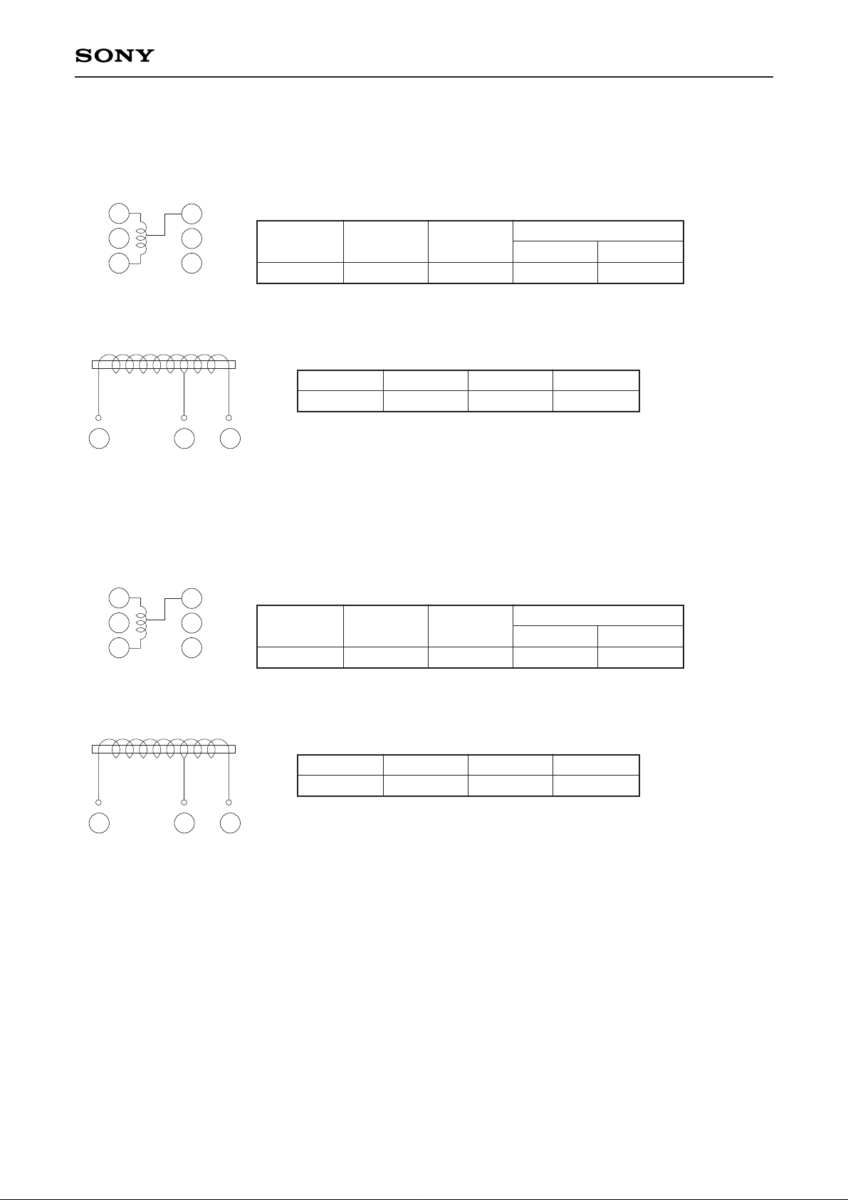
Coil data
APPlication 1
AM OSC
Wire diameter ø 0.08 mm 2UEW
AM Bar Antenna
f (kHz)
796
L (µH)
1 to 3
130
QO
1 to 3
70
1 to 4
32.5
4 to 3
97.5
f (kHz)
796
L (µH)
560
3 to 2
140
2 to 1
420
S
1
2
3
4
5
6
S
1 2 3
Number of widings (µH)
APPlication 2
AM OSC
Wire diameter ø 0.08 mm 2UEW
AM Bar Antenna
f (kHz)
796
L (µH)
1 to 3
210
QO
1 to 3
70
1 to 4
71.3
4 to 3
138.7
f (kHz)
796
L (µH)
900
3 to 2
180
2 to 1
720
S
1
2
3
4
5
6
S
1 2 3
Number of widings (µH)
Page 7

—7—
CXA1600M/P
Application Circuit 1 VARIABLE CAPACITOR used (Equivalent capacitor)
Bar ANT D1, D2: 1S1555 OSC COIL
VARIABLE CAPACITOR:
HQ-025A of Toko Co., Ltd.
or equivalent
D1
D2
C2
4.7µ
130µH
C3
1500p
160p
160p
C7
220µ
3V
GND GND
RF IN OL AGC LO OSC VCC
RF AMP
MIXER OSC
OVERLOAD AGC
BPF
IF AMP
IF DET
AF POWER AMPVOL
VOL
AGC
AGC GND
GNDGND
SP OUT
C1
22µ
100k
R1
2.2µ
C4
0.1µ
C5
C6
220µ
8Ω SP
1 2 3 4
5678
Application circuits shown are typical examples illustrating the operation of the devices. Sony cannot assume responsibility for
any problems arising out of the use of these circuits or for any infringement of third party patent and other right due to same.
Page 8
—8—
CXA1600M/P
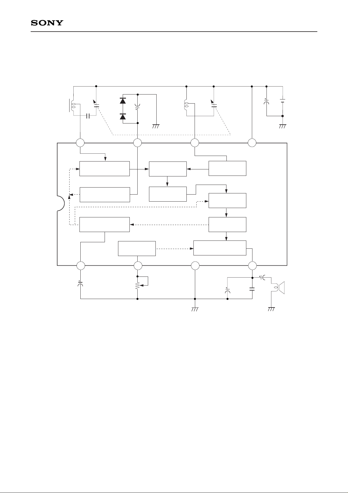
Application Circuit 2 VARIABLE CAPACITOR used (Non-Equivalent capacitor)
Bar ANT D1, D2: 1S1555 OSC COIL
VARIABLE CAPACITOR:
C
RF=160p, COSC=80p
D1
D2
C2
4.7µ
210µH
80p
160p
C7
220µ
3V
GND GND
RF IN OL AGC LO OSC VCC
RF AMP
MIXER
OSC
OVERLOAD AGC
BPF
IF AMP
IF DET
AF POWER AMP
VOL
VOL
AGC
AGC GND
GNDGND
SP OUT
C1
22µ
100k
R1
2.2µ
C4
0.1µ
C5
C6
220µ
8Ω SP
C3
220p
1 2 3 4
5678
Application circuits shown are typical examples illustrating the operation of the devices. Sony cannot assume responsibility for
any problems arising out of the use of these circuits or for any infringement of third party patent and other right due to same.
Page 9

PACKAGE STRUCTURE
PACKAGE MATERIAL
LEAD TREATMENT
LEAD MATERIAL
PACKAGE MASS
EPOXY RESIN
SOLDER/PALLADIUM
42/COPPER ALLOY
0.1g
SOP-8P-L03
SOP008-P-0225
8PIN SOP (PLASTIC)
SONY CODE
EIAJ CODE
JEDEC CODE
0° to 10°
0.1 – 0.1
+ 0.15
0.5 ± 0.2
DETAIL
A
8 5
1
4
4.4 – 0.1
+ 0.3
1.27
1.25 – 0.15
+ 0.4
6.4 ± 0.4
A
5.0 – 0.1
+ 0.4
0.10
PLATING
M
0.24
b
B
(0.15)
0.15 – 0.05
(0.4)
b = 0.4 – 0.05
DETAIL B : SOLDER
0.15 – 0.01
b = 0.4 ± 0.03
DETAIL B : PALLADIUM
+ 0.03
+ 0.1
+ 0.1
SONY CODE
EIAJ CODE
JEDEC CODE
PACKAGE STRUCTURE
PACKAGE MATERIAL
LEAD TREATMENT
LEAD MATERIAL
PACKAGE MASS
EPOXY RESIN
SOLDER PLATING
COPPER ALLOY
8PIN DIP (PLASTIC)
9.4 – 0.1
+ 0.4
2.54
1
4
5
8
1.2 ± 0.15
0.5 ± 0.1
3.0 MIN 0.5 MIN
3.7 – 0.1
+ 0.4
7.62
6.4 – 0.1
+ 0.3
0.25 – 0.05
+ 0.1
0° to 15°
0.5g
DIP-8P-01
DIP008-P-0300
Package Outline Unit : mm
CXA1600M
CXA1600P
CXA1600M/P
—9—
NOTE : PALLADIUM PLATING
This product uses S-PdPPF (Sony Spec.-Palladium Pre-Plated Lead Frame).
 Loading...