

Page 1

—1—
E93313D8X
Sony reserves the right to change products and specifications without prior notice. This information does not convey any license by
any implication or otherwise under any patents or other right. Application circuits shown, if any, are typical examples illustrating the
operation of the devices. Sony cannot assume responsibility for any problems arising out of the use of these circuits.
Recommended Operating Conditions
Supply voltage VCC 2 to 9 V
Structure
Bipolar silicon monolithic IC
Description
The CXA1538M/N/S is high performance one-chip
bipolar ICs designed for FM stereo/AM radios.
These include an FM/AM front end, FM/AM IF
amplifier, FM/AM detection output and FM stereo
demodulator output.
Features
• Low current consumption
(In FM mode ID=11.0 mA, in AM mode 8.5 mA,
VCC=6.0 V)
• Built-in LED drive circuit for tuning
• Built-in LED drive circuit for stereo indicator
• Built-in muting circuit for the FM band
• Few external parts
Absolute Maximum Ratings (Ta=25 °C)
• Supply voltage VCC 14 V
• Operating temperature Topr –10 to +60 °C
• Storage temperature Tstg –55 to +150 °C
• Junction temperature Tjmax 125 °C
• Allowable power dissipation
PD CXA1538M 500 mW
CXA1538N 410 mW
CXA1538S 1050 mW
FM Stereo/AM Radio
CXA1538M CXA1538S
30 pin SOP (Plastic) 30 pin SDIP (Plastic)
Block Diagram
DETUNE
MUTING
CONTROL
TUNING IND
DC
AMP
DC
AMP
BU
AMP
BU
AMP
AUTO
BLEND
MUTING
FM IF/
DISCRI
AM IF/DET
AM FE
REGULATOR
MULTIPLEX
REGULATOR
PD 1
PD 2
1/2 COUNTER
DECODE AMP
RIPPLE FILTER
ST
IND
M/ST
SW
PLL
LPF1
PILOT
DET
LPF2
PILOT
DET
LPF2
ST
IND
VCO
CHECK
Rch
OUT
Lch
OUT
VCC RIPPLE
FILTER
AGC
AFC 1
AGC
AFC 2
GND TUNE
IND
FM IFINAM IFINBAND
SELECT
VCO
GND
PLL
LPF 2
MPX
REG VCOFMDISCRI MUTEAMOSC AFCFMOSC REGFMRF
AM RFINFM RFINFE
GND
FM/AM
FE OUT
FM FE
PD : PHASE DETECTOR
BU : BUFFER
FE : FRONT END
DET : DETECTOR
IND : INDICATOR
1 2 3 4 5 6 7 8 9 10 11 12 13 14 15
161718192021222324252627282930
CXA1538M/N/S
CXA1538N
30 pin SSOP (Plastic)
For the availability of this product, please contact the sales office.
Page 2

—2—
CXA1538M/N/S
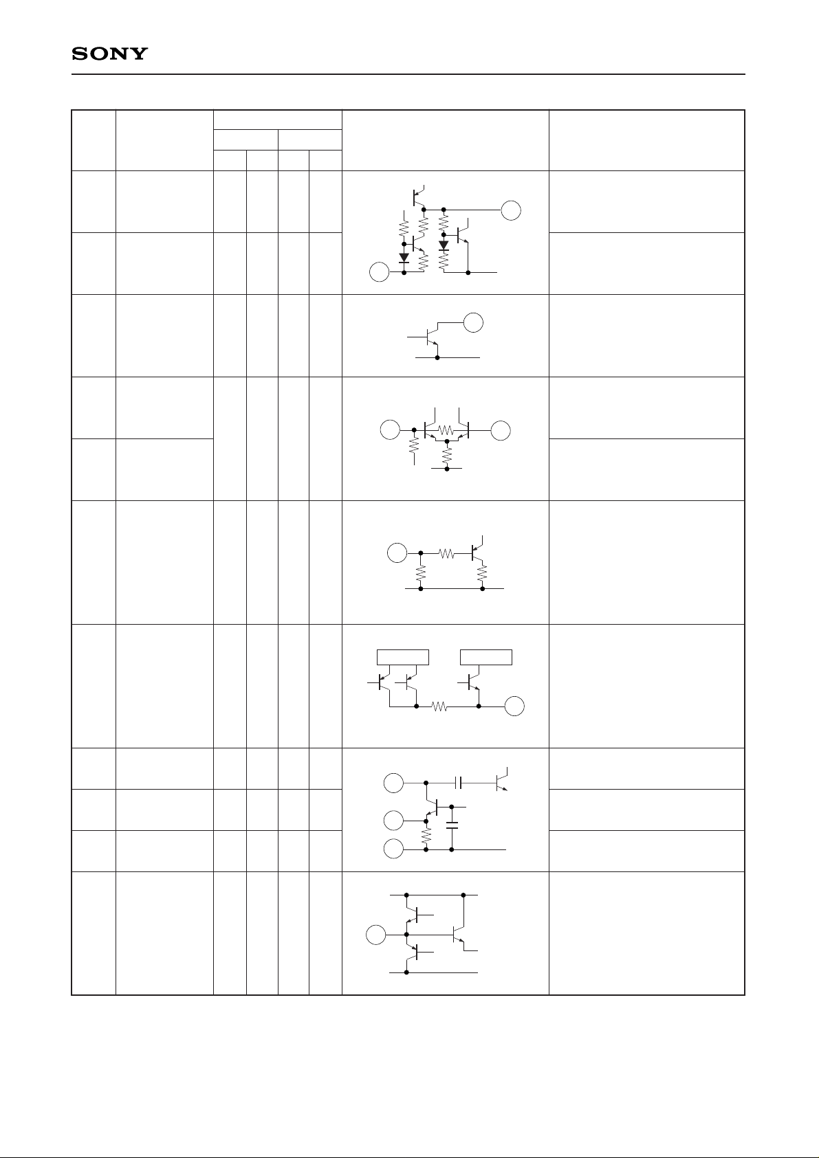
Pin Description and Equivalent Circuit
Pin Voltage (V)
No. Symbol VCC=3 V VCC=6 V Equivalent circuit Description
FM AM FM AM
1
29
2
3
4
5
6
7
8
9
10
PLL LPF1
PLL LPF2
PILOT
DET LPF1
PILOT
DET LPF2
ST IND
VCO CHECK
Rch OUT
Lch OUT
VCC
Ripple
FILTER
AGC/AFC1
AGC/AFC2
0.97 0.97 0.97 0.97
0.95 0.95 0.95 0.95
0.95 0.95 0.95 0.95
1.6 1.6 4.5 4.5
0.66 0.66 1.5 1.5
0.66 0.66 1.5 1.5
3.0 3.0 6.0 6.0
2.7 2.7 4.0 4.0
1.32 1.15 1.32 1.15
1.15 1.47 1.15 1.47
MPX REG
26k26k
129
2
3
MPX REG
6k
VCO
4
5
6
17k
17k
140k
33k
8
22k 50k
3.25k
25k
9
10
LPF for PLL
LPF’s C (1µF) for PILOT DET
inserted between pins 2 and 3
Stereo indicator drive circuit
and output for VCO check
Stereo Rch output pin
Stereo Lch output pin
Supply pin
Ripple filter
AFC pin in J band, determines time
constant of AGC in AM (depending on
external capacitor).
AFC pin in W band, determines time
constant of AGC in AM (depending
on external capacitor).
Page 3
—3—
CXA1538M/N/S
Pin Voltage (V)
No. Symbol VCC=3 V VCC=6 V Equivalent circuit Description
FM AM FM AM
11
25
12
13
15
14
16
17
18
20
19
GND
MUTE
TUNE IND
FM IF IN
BAND
SELECT
AM IF IN
FM/AM
FE OUIT
FE GND
FM RF IN
FM RF
AM RF IN
0 0 0 0
0.05 0.01 0.05 0.01
1.6 1.6 4.5 4.5
1.35 0 1.35 0
0 0 0 0
0.57 0.2 0.8 0.2
0 0 0 0
0.3 0 0.3 0
1.25 1.25 1.25 1.25
1.25 1.25 1.25 1.25
11
25
12
33C
3k
13
15
1k
2k
14
AM Block FM Block
220
16
3p
1k
17
18
20
FE REG
GND
19
GND of FM/AM IF and DET
stage
Time constant for muting
provided
FM/AM tuning indicator drive
circuit
FM IF input pin
FM/AM band switching pin :
AM at GND and FM at OPEN
AM IF input pin
AM/FM IF output pin to
connect with IF filter
GND of FM/AM front end
FM RF amplifier circuit for FM
RF input
FM RF amplifier circuit to
connect to RF tank circuit
AM RF input to connect to bar
antenna
Page 4

—4—
CXA1538M/N/S
Pin Voltage (V)
No. Symbol VCC=3 V VCC=6 V Equivalent circuit Description
FM AM FM AM
21
23
22
24
26
27
28
30
REG
AFC
FM OSC
AM OSC
FM DISCRI
VCO
MPX REG
GND
1.25 1.25 1.25 1.25
1.25 1.25 1.25 1.25
1.25 1.25 1.25 1.25
2.30 2.70 3.60 4.00
1.65 1.65 1.65 1.65
0 0 0 0
1.25V
REG
21
23
REG22REG
24
26
1k
MPX REG
27
28
30
Regulator output
Variable capacitance for AFC
FM local oscillation circuit
AM local oscillation circuit
Phase shift circuit to connect
to ceramic discriminator
VCO control pin for stereo
demodulation
Regulator for MPX
GND of MPX block
Page 5
—5—
CXA1538M/N/S
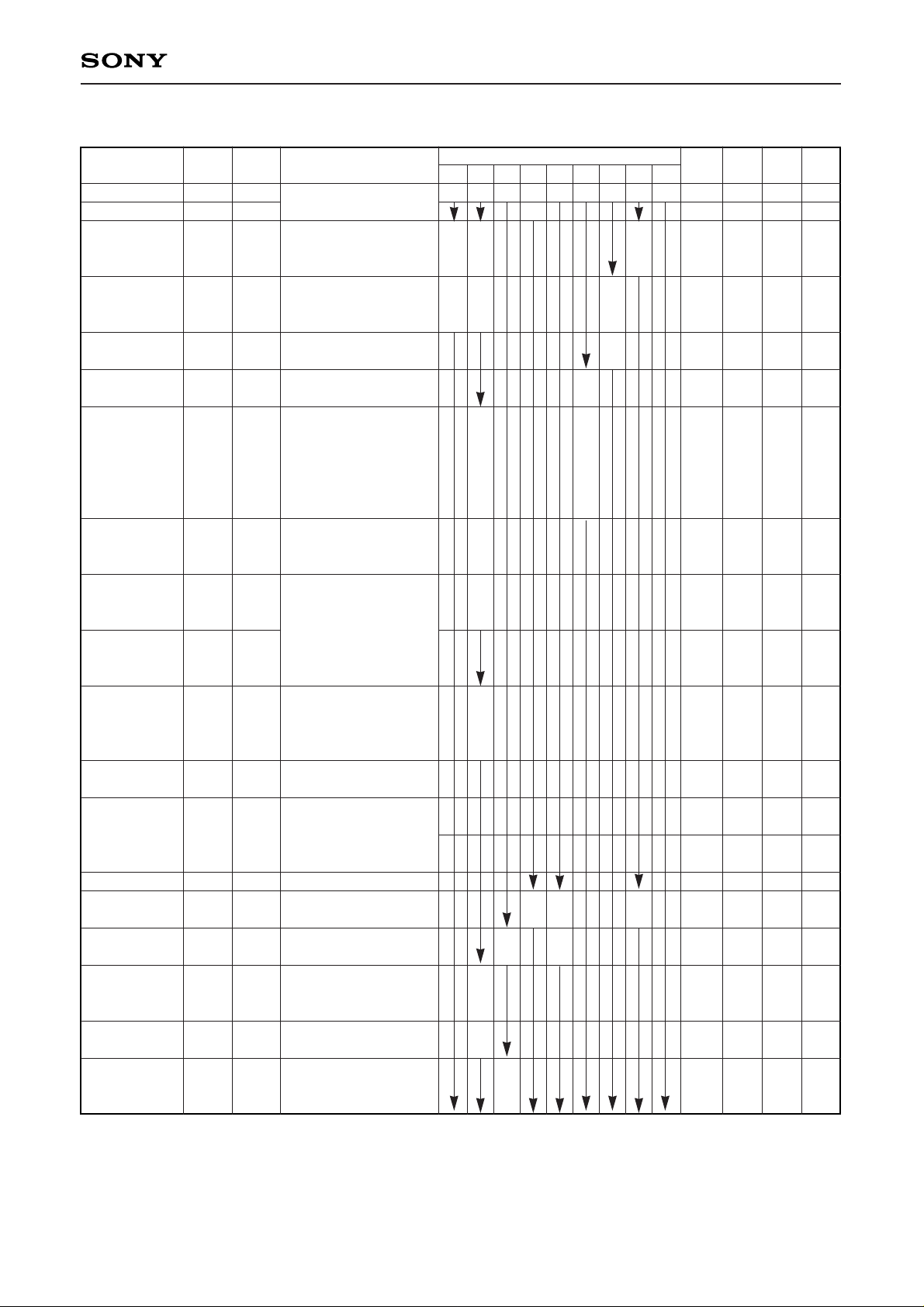
Item
Circuit current (1)
Circuit current (2)
Separation
FM MUTE
STEREO
indicator output
FM front end
voltage gain (1)
FM detection
(MONO/STEREO)
output level L, R
FM-IF
knee level
FM-IF distortion
L, R (MONO)
FM-IF distortion
L, R (STEREO)
FM-IF center
frequency
deviation
FM meter
current (1)
M/ST switching
level by IF input
Auto blend
AM front end
voltage gain (2)
AM-IF
voltage gain (4)
AM detection
output level (L, R)
AM meter
current (2)
AM detection
output distortion
(L, R)
Symbol
ID
1
ID2
SEP
A
1
Is
GV
1
VD1
VD2
THD1
∆F1
IB1
VI1
VI2
GV2
GV3
VD3
IB2
THD2
SW condition
1 2 3 4 5 6 8 9 10
A A A B A B OFF A OFF
A
A
B / B
B
ON
A A /
OFF
OFF
A
A
/ B
B
A
A
/
B
A
B B A
B A
A
/
B
A
A
Test
Point
I
D
ID
VD
VD
Is
V
A
VD
VIN3
VD
V
F
IB
Is
V
IN3
VB
VIN4
VD
IB
VD
Output waveform
and Test method
AM no signal
FM no signal
Separation when V
IN3=
50 dBµV, 10.7 MHz, 1 kHz,
22.5 kHz dev input
Attenuation of noise level
When V
IN3=no signal,
S
8 ON/OFF
V
IN3=60 dBµV, 10.7 MHz CW
Pilot ON
V
IN1=40 dBµV, 100 MHz CW
V
A=10.7 MHz CW
V
IN3=90 dBµV, 10.7 MHz
1 kHz 22.5 kHz dev
V
D=1 kHz sine wave
V
IN3=90 dBµV, 10.7 MHz
Input level at –3 dB of 1 kHz
22.5 kHz dev output
V
IN3=90 dBµV, 10.7 MHz
1 kHz 75 kHz dev
V
D=1 kHz sine wave
V
IN3=90 dBµV, 10.7 MHz CW
V
IN3=60 dBµV, 10.7 MHz CW
V
IN3=10.7 MHz
VIN2=60 dBµV, 1660 kHz CW
V
B=455 kHz CW
V
IN4 level at output of
15.5 mVrms
V
IN4=85 dBµV 455 kHz
(1 kHz 30 % MOD)
V
D=1 kHz sine wave
V
IN4=85 dBµV, 455 kHz CW
V
IN2=95 dBµV, 1660 kHz
(1 kHz 30 % MOD)
V
D=1 kHz sine wave
Electrical Characteristics (Ta=25 °C, VCC=6 V)
Min. Typ. Max. Unit
5.0 8.5 12.0 mA
7.0 11.0 15.0 mA
30 40 — dB
16 23 30 dB
1.8 3.0 5.0 mA
28 35 42 dB
35.0 77.5 138 mVrms
— 25 31 dBµV
— 0.1 2.0 %
0.1 2.0 %
–50 0 +50 kHz
1.8 3.5 7.0 mA
M
→ST
43 48 dBµV
38
ST
→M
41 46 dBµV
35
1 10 41 dB
19 24 28 dB
15 21 29 dBµV
35.0 77.5 138 mVrms
1.3 3.0 7.0 mA
— 0.6 2.0 %
V1 to
V5 input
short
0 dBµV=1 µV
Page 6
—6—
CXA1538M/N/S
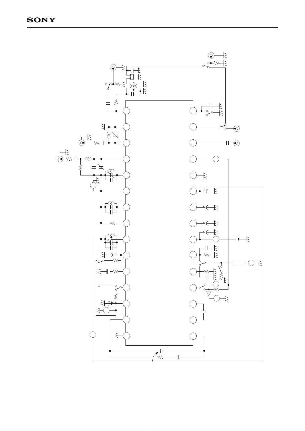
Electrical Characteristics Test Circuit
GND PLL
LPF
MPX
REG
VCO FM
DISCRI
MUTE AM
OSC
AFC FM
OSC
REG FM
RF
AM RF
IN
FM RF
IN
FE
GND
FM/AM
FE OUT
PLL
LPF
PILOT
DET
LPF1
PILOT
DET
LPF2
ST IND
VCO
CHECK
Rch
OUT
Lch
OUT V
CC
RIPPLE
FILTER
AGC/
AFC 1
AGC/
AFC 2 GND
TUNE
IND
FM IF
IN
AM IF
IN
BAND
SELECT
VF
VO
VM
VH
ID
VD
IBIS
0.01µ
0.01µ0.01µ
0.47µ
4.7µ
4.7µ
1µ33µ
100µ
0.01µ
S4
S3
A
A
B
A
A
B
A
B
B
B
S5
2k
VIN 4
AM 455kHz
VIN 3
FM 10.7MHz
7.5k
7.5k
S2
S1
S10
7.5k
30k
15kHz LPF
19kHz
notch
filter
2.2k
10µ
5k
S9
100
CF1
S8
20p
2k
3.3µ
10p
100k
15p
10p
30p
10p
10p
43p
150
100
VIN 2
AM 1660kHz
VIN 1
FM 100MHz
25
18p
2200p
10p
0.01µF
2k
S6
330
V
A
30p
0.01µ
150µH
1µ
VS
1 2 3 4 5 6 7 8 9 10 11 12 13 14 15
161718192021222324252627282930
Page 7
—7—
CXA1538M/N/S
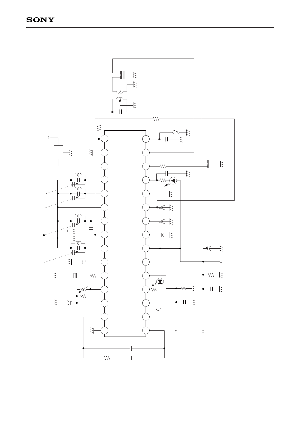
Application Circuit
Note)
This circuit is an application example and is not guaranteed for all applications.
For C, R (C13, C14, R6, R7) marked∗, refer to “2. MPX circuit” of “Notes on Usage.”
C9
10µ
CF3
RV
22k
R3
10k
C8
3.3µ
R4
2.2k
C11
4.7µ
C10
0.47µ
GND PLL
LPF
MPX
REG
VCO FM
DISCRI
MUTE AM
OSC
AFC FM
OSC
REG FM
RF
PLL
LPF
PILOT
DET
LPF1
PILOT
DET
LPF2
ST IND/
VCO
CHECK
Rch
OUT
Lch
OUT V
CC
RIPPLE
FILTER
AGC/
AFC 1
AGC/
AFC 2 GND
TUNE
IND
FM IF
IN
AM IF
IN
BAND
SELECT
AM RF
IN
FM RF
IN
GND FM/AM
FE OUT
C12
1µ
R ch OUT
L ch OUT
∗C13
0.022µ
∗C14
0.022µ
C15
100µ
C16
33µ
C17
1µ
C18
4.7µ
R10
330
R1
100k
C19
0.01µ
C20
0.01µ
∗R6
3.3k
∗R7
3.3k
V
CC=3V
R5
2.2k
R8
2.2k
S1
IFT CF1
R2
2.2k
BPF
C4
4PF
L4
L3C3
18p
C2
2.0p
C7
3p
C1
7p
L2L1
C6
10µ
C5
0.001µ
CF2
BPF
CF1
CF2
CF3
IFT
: FM BAND PASS FILTER
: AM 455kHz CF
: FM 10.7MHz CF
: FM DISCRIMINATOR
: AM 455kHz IFT
R9
100
1 2 3 4 5 6 7 8 9 10 11 12 13 14 15
161718192021222324252627282930
Capacitor unit : F
Application circuits shown are typical examples illustrating the operation of the devices. Sony cannot assume responsibility for
any problems arising out of the use of these circuits or for any infringement of third party patent and other right due to same.
Page 8
—8—
CXA1538M/N/S
Input signal level (dBµV)
Separation/response (dB)
Distortion T
HD1 (%)
Input signal level (dBm)
Response (dB)
Distortion THD2 (%)
0
–10
–20
–30
–40
–50
–60
0
–10
–20
–30
–40
–50
–60
5
4
3
2
1
5
4
3
2
1
10 20 30 40 50 60 70 80 90 100 110
10 20 30 40 50 60 70 80 90 100 110
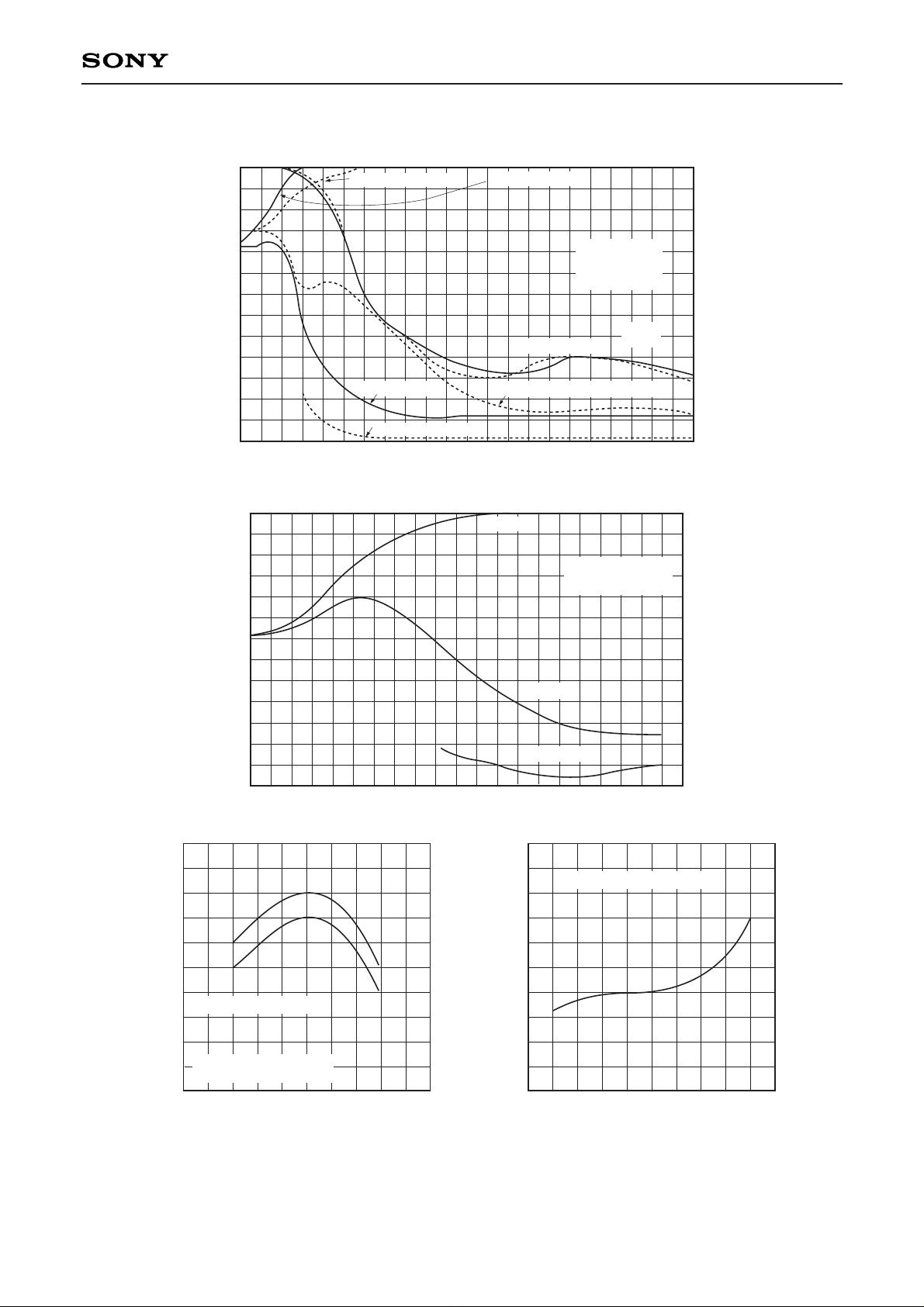
FM I/O characteristics
AM I/O characteristics
SIGNAL (STEREO)
SIGNAL (MONO)
VCC
FREO
MODE
DEV
3V
98MHz
400Hz
22.5kHz
VCC
FREO
MOD
3V
1000kHz
400Hz, 30%
SEPARATION
L → R
R → L
NOISE(STEREO) (WITH LPF)
NOISE(MONO)
DISTORTION(MONO)
SIGNAL
DISTORTION
NOISE
73 74 75 76 77 78 79
45
40
VCO - free-running frequency (kHz)
VCO - free-running frequency (kHz)
Separation (dB)
0 20 40
60 80
79
78
77
76
75
Ta - Ambient temperarure (°C)
Vin3=90dBµV 10.7MHz
fmod = 1kHz 22.5kHz dev
Pilot ON
Vin3=90dBµV 10.7MHz CW
Page 9
—9—
CXA1538M/N/S
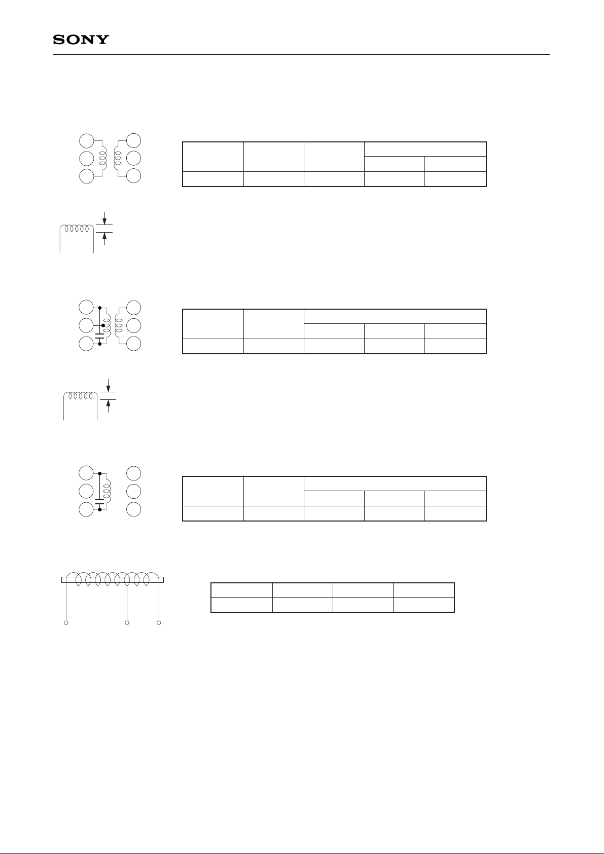
Coil data
AM OSC
Core diameter ø 0.06 mm 2 UEW
Equivalent to L-5K7H5 R12-1684X, Mitsumi Electric Co., Ltd. or
7TRS-8441 TOKO Co., Ltd.
f (kHz)
796
L (µH)
1 to 3
270
QO
1 to 3
125
1 to 3
107
4 to 6
29
S
1
2
3
4
5
6
φ 5mm
φ 6mm3.5t
Number of widings (t)
AM Bar Antenna
f (kHz)
796
L (µH)
650
Primary
91 t
Secondary
20 t
PRIMARY
SECONDARY
FM RF
AM IFT
Core diameter ø 0.07 mm UEW
Equivalent to 21K7H5 R12-8558A, Mitsumi Electric Co., Ltd. or
7MC-7789N TOKO Co., Ltd.
CO (pF)
1 to 3
180
QO
1 to 3
90
1 to 2
111
2 to 3
35
4 to 6
7
S
1
2
3
4
5
6
φ 4mm
φ 0.6mm3.5t
Number of widings (t)
FM Discriminator
Core diameter ø 0.1 mm 2 UEW
Equivalent to 119ASC-12200Z, TOKO Co., Ltd.
CO (pF)
1 to 3
82
QO
1 to 3
95
1 to 3
111
1
2
3
4
5
6
Number of widings (t)
FM OSC
PFWE8
BPF (88 to 108 MHz) Soshin Electric Co., Ltd.
CF1 SFU-455B Murata Mfg. Co., Ltd. or BFCFL-455 TOKO Co., Ltd.
CF2 SFE10.7MA5 Murata Mfg. Co., Ltd.
CF3 CDA10.7MG1 Murata Mfg. Co., Ltd.
VC PVC2LXT16L Mitsumi Electric Co., Ltd.
VC (Rear Mount) HU22124N700 TOKO Co., Ltd.
PVC2LXT16B Mitsumi Electric Co., Ltd.
Page 10

—10—
CXA1538M/N/S
Notes on Usage
1. VCO free run frequency adjustment method
As this IC has built-in oscillation capacitance, the oscillation frequency can be controlled with an external
resistor.
1) VCO Adjustment Method
Pin 4 is the stereo indicator and VCO check pin. Therefore, in stereo mode (when stereo indicator drive
Tr Q2 is switched on), pin 4 voltage lowers down, Q1 is cut off and VCO oscillation waveform can not be
seen. In AM mode as well, the oscillation waveform can not be seen as VCO turns off.
Adjust the free run frequency at 76 kHz ±50 Hz.
In this IC, tuner and MPX sections are directly connected. Therefore, free run frequency is not stable, being
affected by noise except in reception mode. For free run adjustment, input signals from either RF or IF.
(Input signal should be RF [Tuning frequency] or fo of the discriminator using IF (10.7 MHz) and input
more than 60 dBµ.)
2) How to Deal with pin 4 After Adjustment.
With the use of a stereo indicator. When VCC is 3 V or more, insert a bypass resistance
R to prevent LED malfunction.
Without the use of a stereo indicator.
Turn pin 4 to open or connect to GND.
3) Control Resistor of VCO Oscillation Frequency
For the VCO control resistor of this iC, a carbon film resistor suffices.
For easier adjustment of temperature characteristics and VCO free run frequency, the following
combination is recommended.
27 28
10k
22k
Capacitor for decoupling
Q1 Q2
33k
VCC
about 180mVp-p
4
2.2k
V
CC=3V
4
OPEN
4 4
27 28
10k
22k
2.2k
R
V
CC>3V
4
Page 11

—11—
CXA1538M/N/S
2. MPX circuit
1) MPX load resistance
When power supply voltage is over 3 V, change the MPX load resistor R6, R7 from 3.3 kΩ to 6.8 kΩ.
In this case, the output level is increased by about 6 dB.
2) Time constant of de-emphasis
Refer to the following table as the time constant is determined at C13, C14, R6 and R7.
3. AFC circuit
1) This IC has a built-in variable capacitances.
Change to the following circuit when designing J band, because the standard circuit is for W band.
2) AFC pull-in range is expanded by increasing the capacitance of standard circuit C7 3 pF.
Adjust the value of capacitance according to the set specification.
4. Auto blend circuit
This IC has a built-in auto blend circuit and a MONO switch is not required as a rule. This circuit controls
the separation in proportion to the signal level and reduces noise automatically for stereo reception below
the mid electric field when the electric field strength reaches lower than about 40 dBµ. When the electric
field strength turns below 10 to 15 dBµ, MONO operation is automatically activated.
To switch MONO mode on externally, ground pin 3 with 33 kΩ.
50 µs
75 µs
3.3 kΩ
0.015 µF
0.022 µF
6.8 kΩ
0.0082 µF
0.012 µF
R6, R7
C13, C14
3pF
1µ
1µ
4.7µ
150k
9 10
2223
33k
MONO
SW
2 3
Page 12
—12—
CXA1538M/N/S
5. FM discriminator
For FM detection, the quadrature detection system is adopted. As a phase shifter, a ceramic resonator (CF
3 discriminator) applies to achieve adjustment-free detection. Though the sensitivity and selectability will be
slightly affected, the discriminator can be replaced by a coil as shown below. Combining CF2 (FMIF) and
CF3 (PM discriminator) poses problems with the distortion factor when deviation with the IF band central
frequency fo occurs. To this effect, use pairs of the same rank as indicated in the chart.
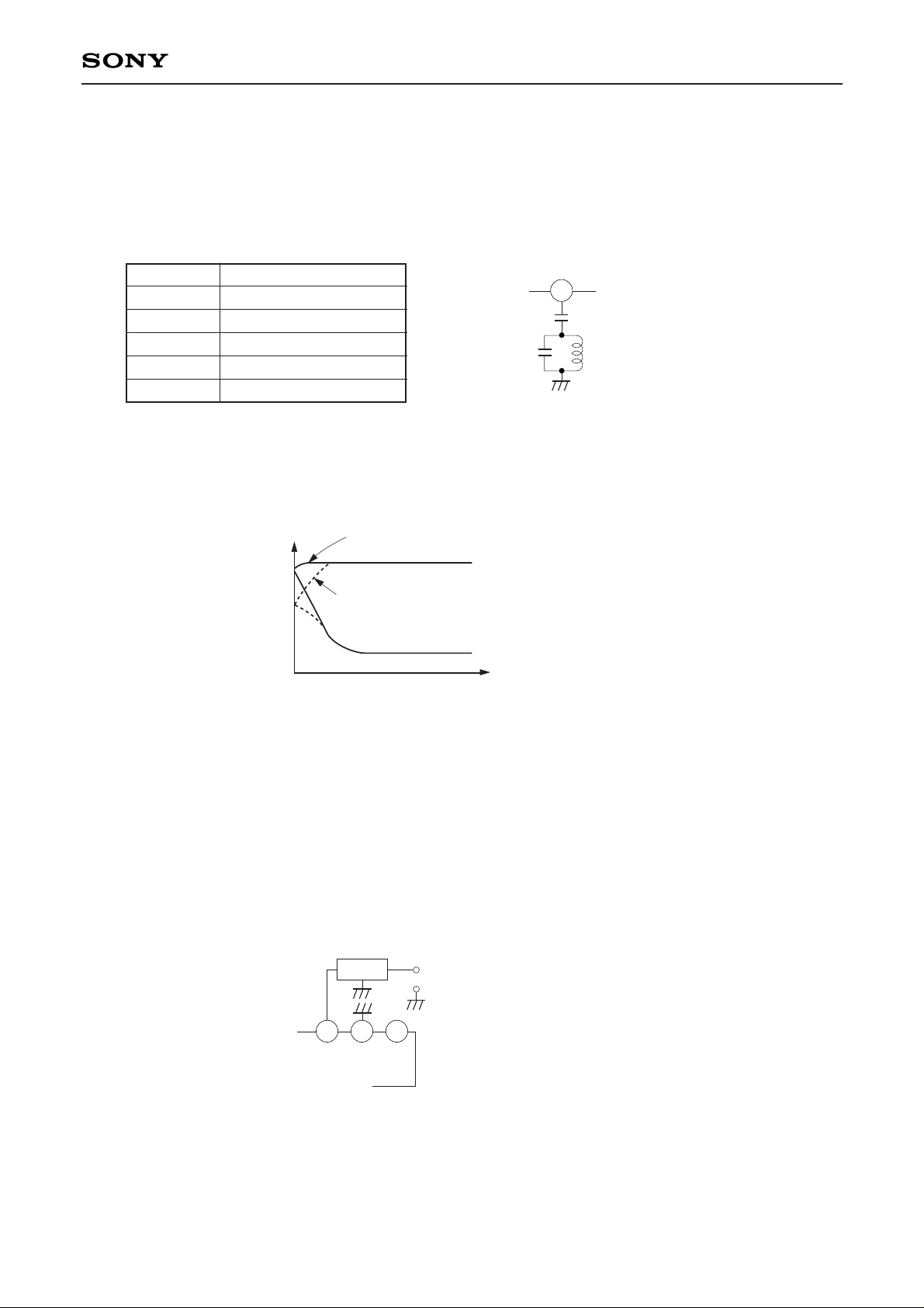
6. FM muting circuit
This IC has a built-in soft muting circuit.
As shown in the following I/O characteristics diagram, 23 dB (Typ.) muting is applied and noise level
reduced during weak electric field and out of tune instances.
7. Notes on patterns
1) Positions of FM ANT and OSC coils
Locate those at right angles to each others to avoid inductance M through coupling. Further, insert a pin
21 pattern between patterns of pins 22, 20 and coils.
2) Tuning circuit
As the capacitances C1 to C4, L2 and L3 are the constants on the standard circuit board, check the
constants when a new circuit board is used.
3) Grounding pins
Pin 17 is a grounding pin for AM, FM and FE ; pin 11 for IF ; and pin 30 for MPX. Use as thick as
possible a pattern since the grounding between ANT IN, BPF and pin 17 significantly stability, NF and
characteristics affects.
4) Ground bypass capacitors C5 (0.001 µF) and C6 (10 µF) connected to pin 21 as close as possible to pin
17.
A Red
B Blue
C Orange
D Black
E White
fO of CF2 and CF3
10.70 MHz
10.67 MHz
10.73 MHz
10.64 MHz
10.76 MHz
22pF
DISCRI
COIL
26
Conventional IC
IC with built-in soft MUTE
S+N
N
INPUT LEVEL (dBµ)
RESPONSE (dB)
3
–23
ANT
IN
1618
BPF
17
Page 13
—13—
CXA1538M/N/S
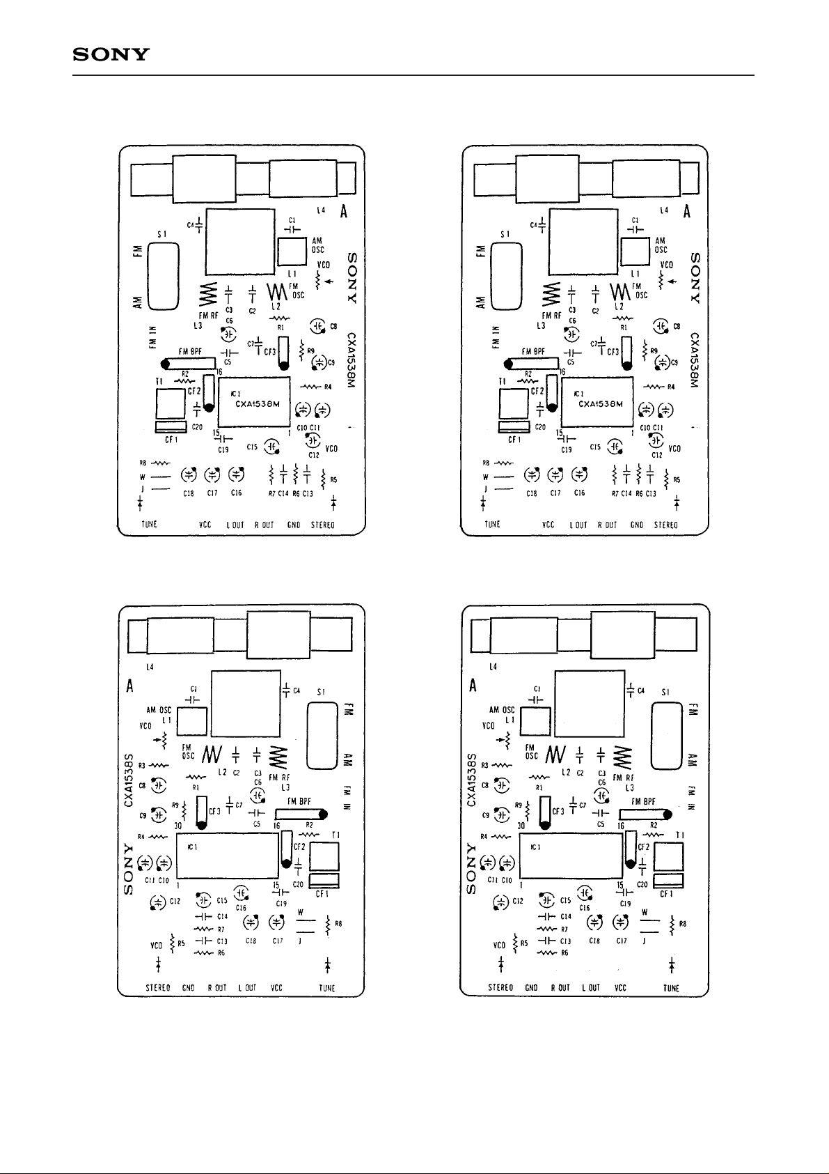
CXA1538M
CXA1538S
Page 14
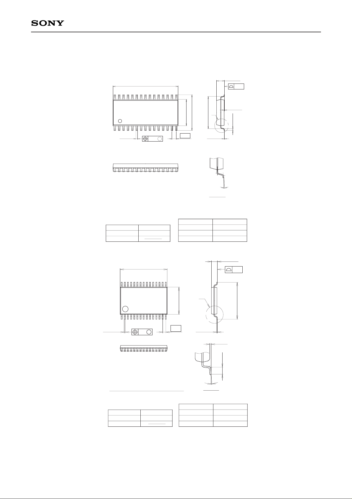
Package Outline Unit : mm
CXA1538M
CXA1538N
CXA1538M/N/S
—14—
0.45 ± 0.1
1
1.27
15
7.6 – 0.1
+ 0.3
10.3 ± 0.4
16
30
18.8 – 0.1
+ 0.4
0.2
M
0.1
0.2 – 0.05
+ 0.1
0.5 ± 0.2
0.1 – 0.05
A
(9.3)
2.3 – 0.15
+ 0.4
30PIN SOP(PLASTIC)
SONY CODE
EIAJ CODE
JEDEC CODE
SOP-30P-L03
SOP030-P-0375
PACKAGE MATERIAL
LEAD TREATMENT
LEAD MATERIAL
PACKAGE MASS
EPOXY RESIN
SOLDER PLATING
COPPER ALLOY
PACKAGE STRUCTURE
0.7g
0° to 10°
+ 0.2
DETAIL A
SONY CODE
EIAJ CODE
JEDEC CODE
PACKAGE STRUCTURE
PACKAGE MATERIAL
LEAD TREATMENT
LEAD MATERIAL
PACKAGE MASS
EPOXY RESIN
SOLDER/PALLADIUM
42/COPPER ALLOY
30PIN SSOP (PLASTIC)
∗9.7 ± 0.1
∗5.6 ± 0.1
0.65
0.22 – 0.05
30
1 15
16
1.25
+ 0.2
– 0.1
7.6 ± 0.2
0.15
+ 0.05
– 0.02
0.1 ± 0.1
0.5 ± 0.2
0° to 10°
A
DETAIL A
SSOP-30P-L01
SSOP030-P-0056
0.1g
NOTE: Dimension “∗” does not include mold protrusion.
PLATING
0.10
0.13
M
+ 0.1
NOTE : PALLADIUM PLATING
This product uses S-PdPPF (Sony Spec.-Palladium Pre-Plated Lead Frame).
Page 15
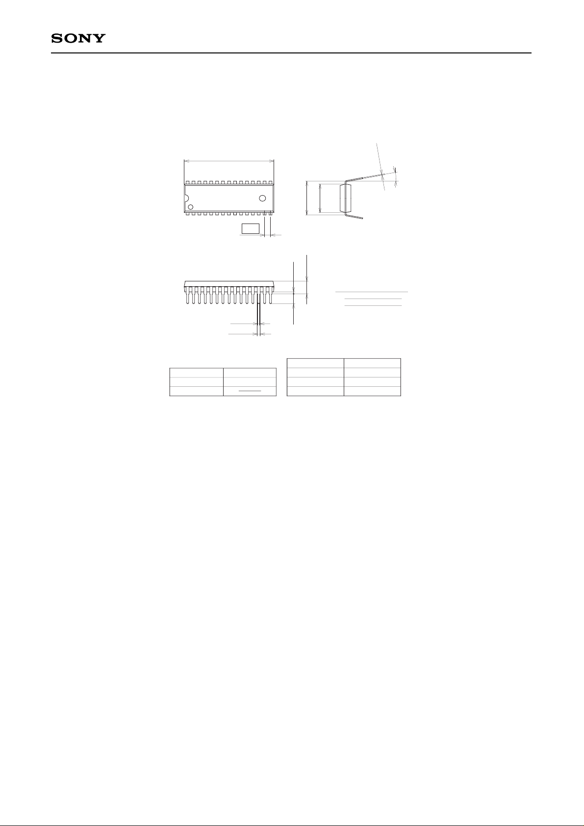
SONY CODE
EIAJ CODE
JEDEC CODE
30PIN SDIP (PLASTIC)
26.9 – 0.1
+ 0.4
15
16
30
1.778
10.16
8.5 – 0.1
+ 0.3
0.25 – 0.05
+ 0.1
0° to 15°
0.5 ± 0.1
0.9 ± 0.15
3.0 MIN
0.5 MIN
3.7 – 0.1
+ 0.4
SDIP-30P-01
SDIP030-P-0400
1
PACKAGE STRUCTURE
MOLDING COMPOUND
LEAD TREATMENT
LEAD MATERIAL
PACKAGE MASS
EPOXY RESIN
PLATING
COPPER ALLOY
1.8g
SOLDER/PALLADIUM
1.All mat surface type.
Two kinds of package surface:
2.All mirror surface type.
CXA1538S
CXA1538M/N/S
—15—
NOTE : PALLADIUM PLATING
This product uses S-PdPPF (Sony Spec.-Palladium Pre-Plated Lead Frame).
 Loading...