

Page 1
CXA1391Q/R
Processing IC for Complementary Color Mosaic CCD Camera
Description
The CXA1391Q/R is a bipolar IC developed for
signal processing in complementary color mosaic
CCD cameras.
Features
• Low power consumption (170mW)
• Number of delay lines used for signal processing
can be selected according to the system
requirements
• The LPF peripheral to 1H delay line is built in
Structure
Bipolar silicon monolithic IC
Applications
Complementary color mosaic CCD cameras
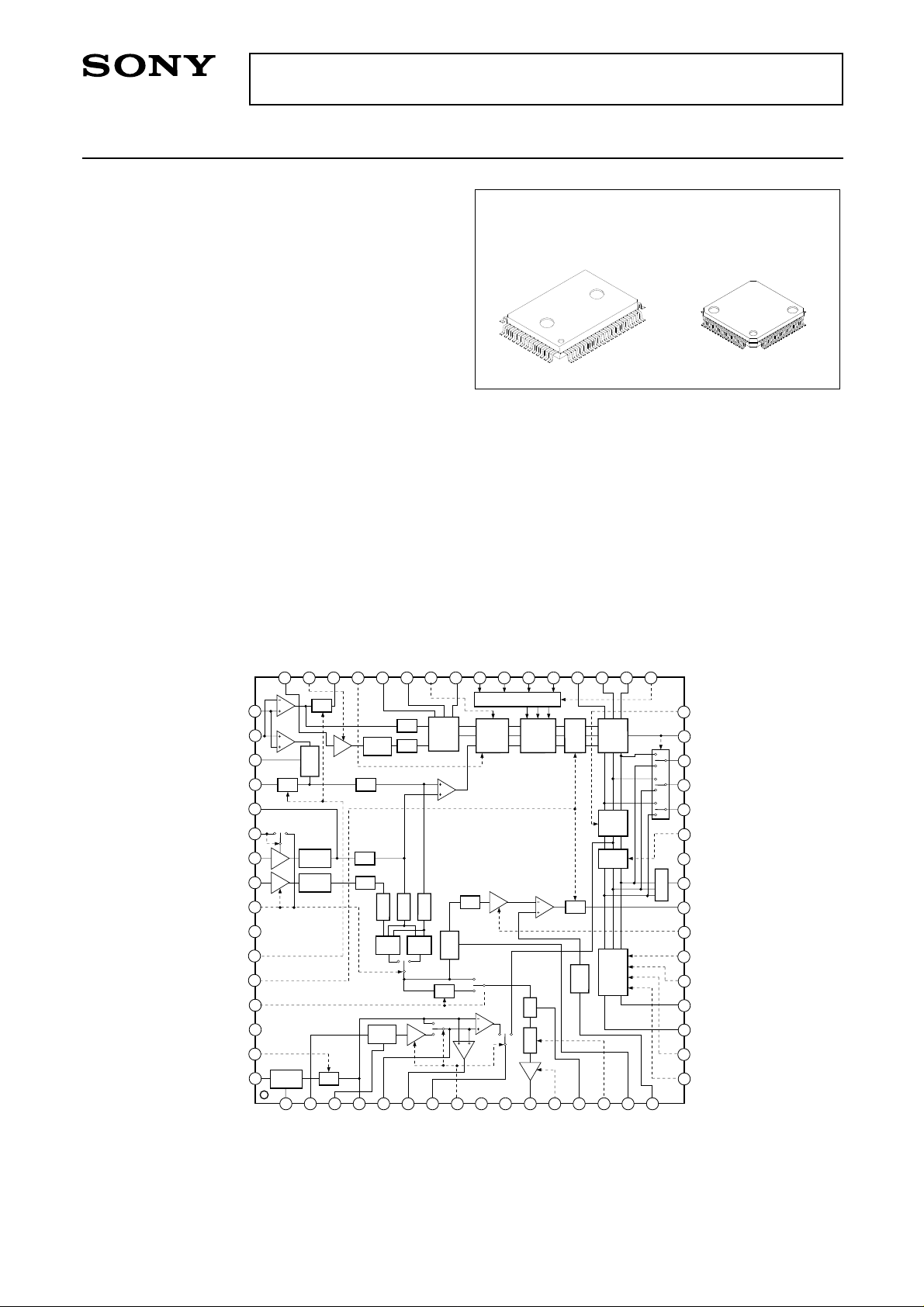
Block Diagram and Pin Configuration
(Top View)
CXA1391Q
64 pin QFP (Plastic)
CXA1391R
64 pin LQFP (Plastic)
Absolute Maximum Ratings
• Supply voltage Vcc 7 V
• Storage temperature Tstg –55 to +150 °C
• Allowable power dissipation
PD 690 mW
(LQFP: Ta = 25°C, without P.C.B)
Recommended Operating Conditions
• Supply voltage Vcc 4.75 to 5.25 V
• Ambient temperature Topr –20 to +75 °C
C LEVEL
CLF C R
CLP C G
CLP C B
R GAIN
R CONT
B CONT
B GAIN
ID
B MTX
CLP C MPX2
CLP C MPX1
R MTX
DLCO OUT
C1 GAIN
S2 IN
S1 IN
CLP C Y O
DLY0 OUT
DLY1 OUT
Y1 GAIN
DLY1 IN
DLY2 IN
Y2 GAIN
GND 2
LPF ADJ 1
LPF ADJ 2
LPF ADJ 3
VCC
Y-r CONT
YH IN
DLC1 IN
46
CLP
CLP
CLP
2
(CLP4)
Y0
DLYH IN
LPF
45
GC
Y1
Y2
YH1
YH0
r
3
CLP C DLYH
48
47
LPF
GC
GC
CLP
(CLP2)
C0
Y0
(CLP4)
(CLP4)
1
CLP C Y H
49
50
51
52
53
54
55
56
57
58
59
60
61
62
63
64
LPF
LPF
LPF
4
CLP
(CLP4)
(CLP4)
DLYH OUT
44
–
3H
APCN
CLP
5
43
C0
LPF
C1
LPF
Y0
Y1
Y1
Y0
Y2
KNEE
KNEE
KNEE
–
–
2H
APCN
V-APCN
YH0
GC
YH1
6
YH OUT 2
YH OUT 1
CLP
(CLP2)
&
MPX
LPF
7
TP
40
-CB
ABS
(CLP4)
8
DLYH GAIN
CR
Y
39
WB CONTROL
MATRIX
GC
9
10
CLP4
4142
V-APCN
CLP
B
G
WB AMP
R
CS VAP
CS-Y
V-APCN
G ch SLICE
CLP2
37
38
MAX
CLP
SLICE
GC
12
11
VAP OUT
35
36
LPF
LPF
CS
CLP
(CLP4)
CS-Y
13
14 15
VAP GAIN
CLP C VAP
CLP
(CLP2)
R-WB
G-WB
SLICE
r
R-r
G-r
MTX
R-Y
B-Y
VAP SLICE
33
34
32
C SLICE
WB DC
31
WB B
B-WB
B-r
Hue & GC
B-Y
R-Y
CLP C CS
30
B-r
WB G
29
G-r
WB R
28
R-r
C-r CONT
27
GND 1
26
YL OUT
25
YL MTX
CS OUT
24
CS GAIN
23
R – Y HUE
22
B – Y HUE
21
R – Y OUT
20
B – Y OUT
19
B – Y GAIN
18
R – Y GAIN
17
16
CS IN
Sony reserves the right to change products and specifications without prior notice. This information does not convey any license by
any implication or otherwise under any patents or other right. Application circuits shown, if any, are typical examples illustrating the
operation of the devices. Sony cannot assume responsibility for any problems arising out of the use of these circuits.
– 1 –
E89Z18-ST
Page 2
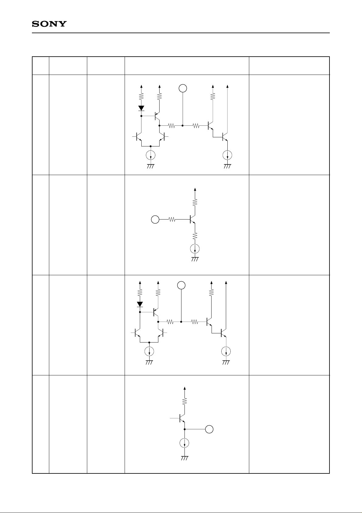
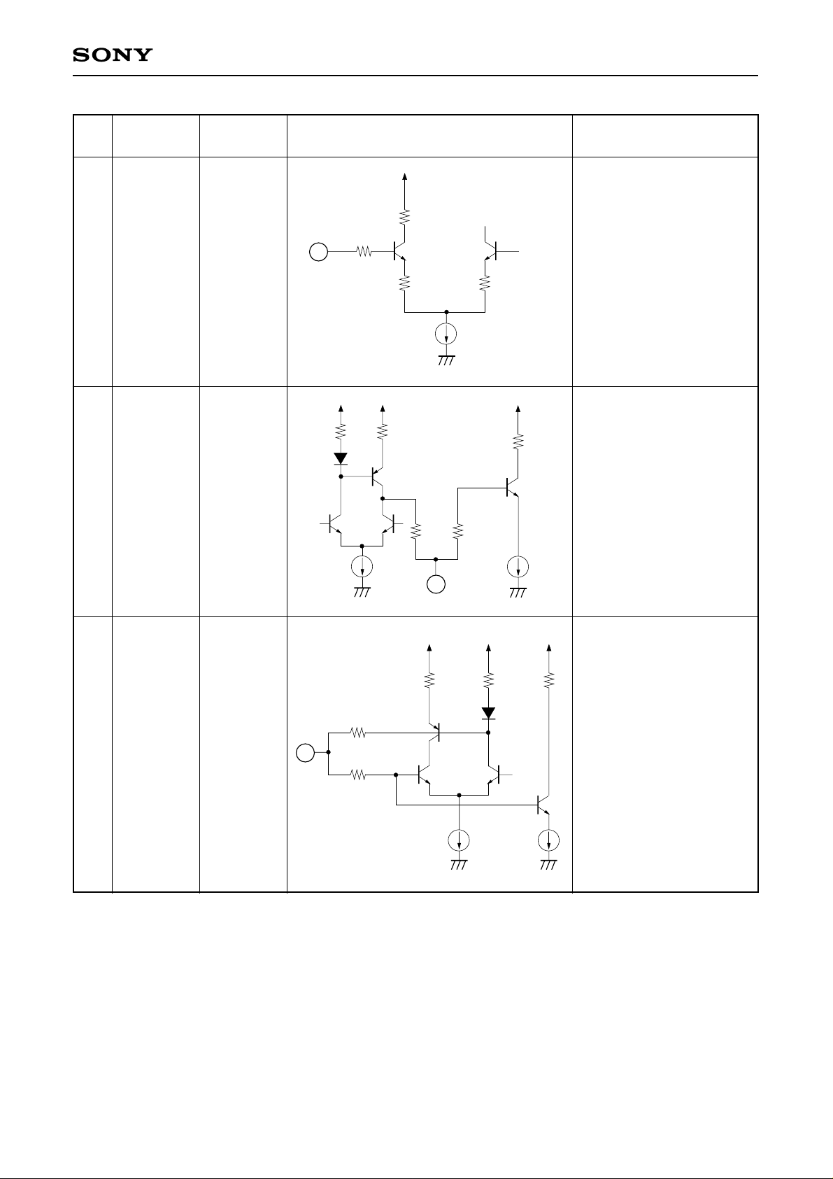
Pin Description
CXA1391Q/R
PIn
No.
1
2
Symbol
CLP C YH
DL YH IN
Pin voltage
3 to 3.5V
3.65V
2.4k 2.4k
Equivalent circuit Description
1
800
1k 147
Capacitor connecting pin
for YH clamp
(Clamp at CLP2)
180µA 80µA
1k
147
2
5k
80µA
DL YH signal input pin
(Input from 1H delay line)
Sig: Typ. 200mV
(Positive polarity)
3
200
1k
Capacitor connecting pin
for DL YH clamp
(Clamp at CLP4)
40µA
DL YH signal output pin
2.6k 2.6k
CLP C
3
DL YH
2.6 to 3.8V
1k 147
180µA
(To 1H delay line)
DL YH
4
OUT
2.7 to 3.1V
4
Sig: Typ. 400mV
Max. 600mV
400µA
(Negative polarity)
Note) Pin voltage for input and output pins indicate black level.
– 2 –
Page 3
CXA1391Q/R
PIn
No.
5
6
Symbol Pin voltage Equivalent circuit Description
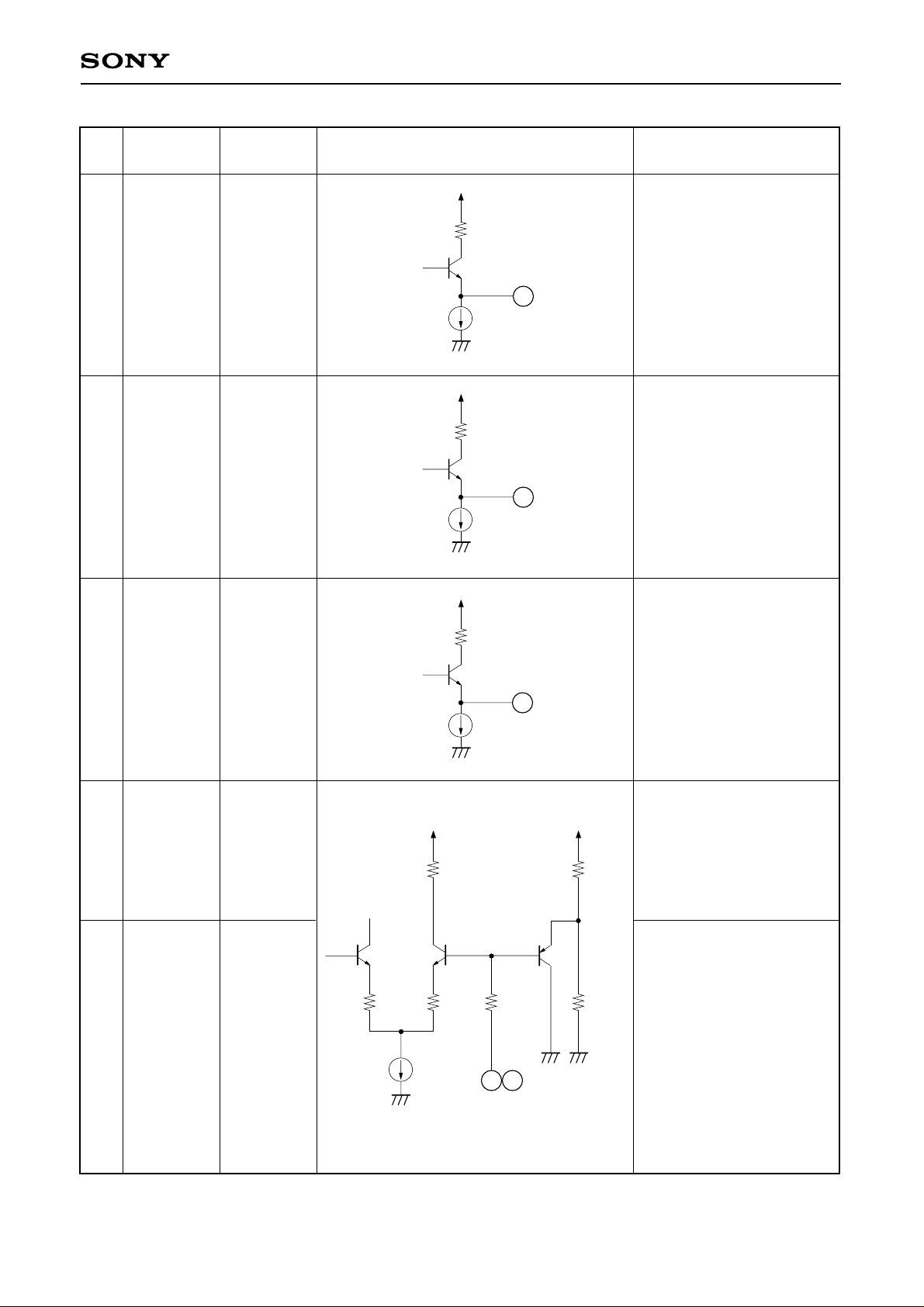
YH OUT1
YH OUT2
100
1.9 to 2.3V
5
160µA
100
1.9 to 2.3V
6
400µA
YH1 signal output pin
Sig: Typ. 1V
Max. 1.5V
(Positive polarity)
YH2 signal output pin
Sig: Typ. 1V
Max. 1.5V
(Positive polarity)
7
8
54
TP
DL YH GAIN
Y1 GAIN
2.6 to 3.0V
(YH)
2.5 to 2.9V
(G)
0V
(0H Mode)
1.8 to 5V
(1H Mode)
0V:
Common
control by
Pin 57
1.8 to 5V
Independent
control
30k
500
7
80µA
1k
30k 147 100k
40µA
8
54
100k
TP OUT (adjusting pin)
1H mode: Outputs YH1–YH0
0H mode: Outputs Gch
C-slice OUT
(Mode selection is executed
through Pin 8)
DL YH signal gain control
pin
(For 1H delay line gain
compensation of YH)
TP (Pin 7) mode selection
0H Mode: 0V
1H Mode: 1.8 to 5V
DLY1 signal gain control pin
(1H delay line gain
compensation)
0V: DLY1 signal gain
control is executed in
common with DLY2
signal gain control.
1.8 to 5V: DLY1 signal gain
control is executed
independently from
DLY2 signal gain
control.
– 3 –
Page 4
CXA1391Q/R
PIn
No.
9
10
11
Symbol Pin voltage Equivalent circuit Description
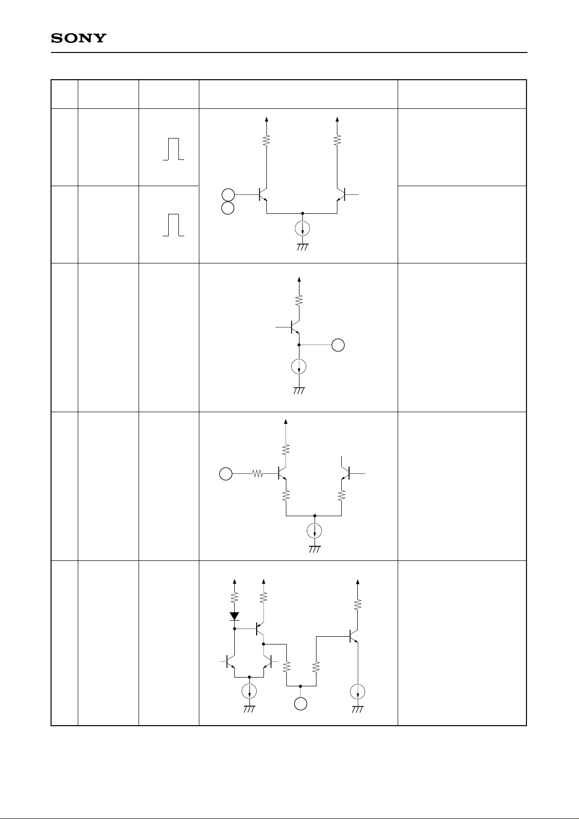
CLP4 pulse input pin
CLP4
CLP2
5V
0
5V
0
9
10
40µA
431
30k1k
(BLK clamp)
(CMOS level input,
VTH = 2.5V)
CLP2 pulse input pin
(OPB clamp)
(CMOS level input,
VTH = 2.5V)
V-APCN signal output pin
VAP OUT
2.6 to 3.0V
280µA
11
Sig: Max. 1.2Vp-p
∗
12
13
VAP GAIN
CLP C VAP
1.8 to 5V
(Control)
3.4 to 3.8V
1k
147
12
25k
2.6k 2.6k
147
180µA
13
40µA
147
25k
V-APCN signal output level
adjustment pin
1k
Capacitor connecting pin
for VAP clamp
(Clamp at CLP4)
12µA
∗
V-APCN: Vertical Aperture Compensation
– 4 –
Page 5
CXA1391Q/R
PIn
No.
14
15
Symbol Pin voltage Equivalent circuit Description
1k
147
VAP SLICE
1.8 to 5V
(Control)
14
2.6k
30k
2.6k
30k
40µA
1k
V-APCN signal
dark slice volume
adjustment pin
Capacitor connecting pin
CLP C CS
3.5 to 3.7V
for CS clamp
(Clamp at CLP4)
147
147
180µA
15
20µA
16
CS IN
C-Couple
input
2.9 to 3.3V
16
147
147
2.6k 2.6k
1k
AGC CS signal input pin
Sig: Max. 1V
20µA180µA
– 5 –
Page 6
CXA1391Q/R
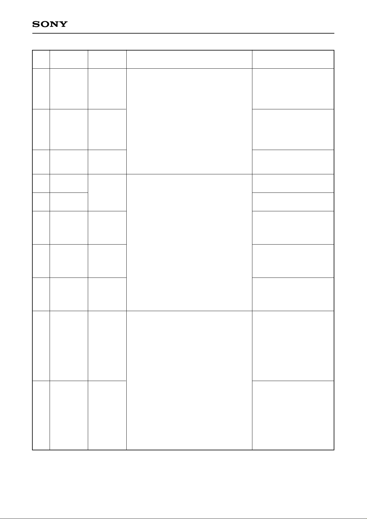
17
18
23
19
20
46
R–Y GAIN
B–Y GAIN
CS GAIN
B–Y OUT
R–Y OUT
DLC0 OUT
0V:
R–G output
1.8 to 5V:
R–Y output
0V:
B–G output
1.8 to 5V:
B–Y output
1.8 to 5V
(Control)
2.75 to 3.15V
(Hue OFF)
2.35 to 2.75V
(Hue ON)
1.8 to 2.2V
R–Y signal output level
adjustment pin
Pin 20 Mode select
0V: R–G output
1.8 to 5V: R–Y output
B–Y signal output level
adjustment pin
Pin 19 Mode select
0V: B–G output
1.8 to 5V: B–Y output
V-APCN CS signal
gain control pin
52
53
21
DLY0 OUT
DLY1 OUT
B–Y Hue
1.4 to 1.8V
2.8 to 3.2V
0V:
B–Y hue control pin
R–Y hue control pin
– 6 –
Page 7
CXA1391Q/R
PIn
No.
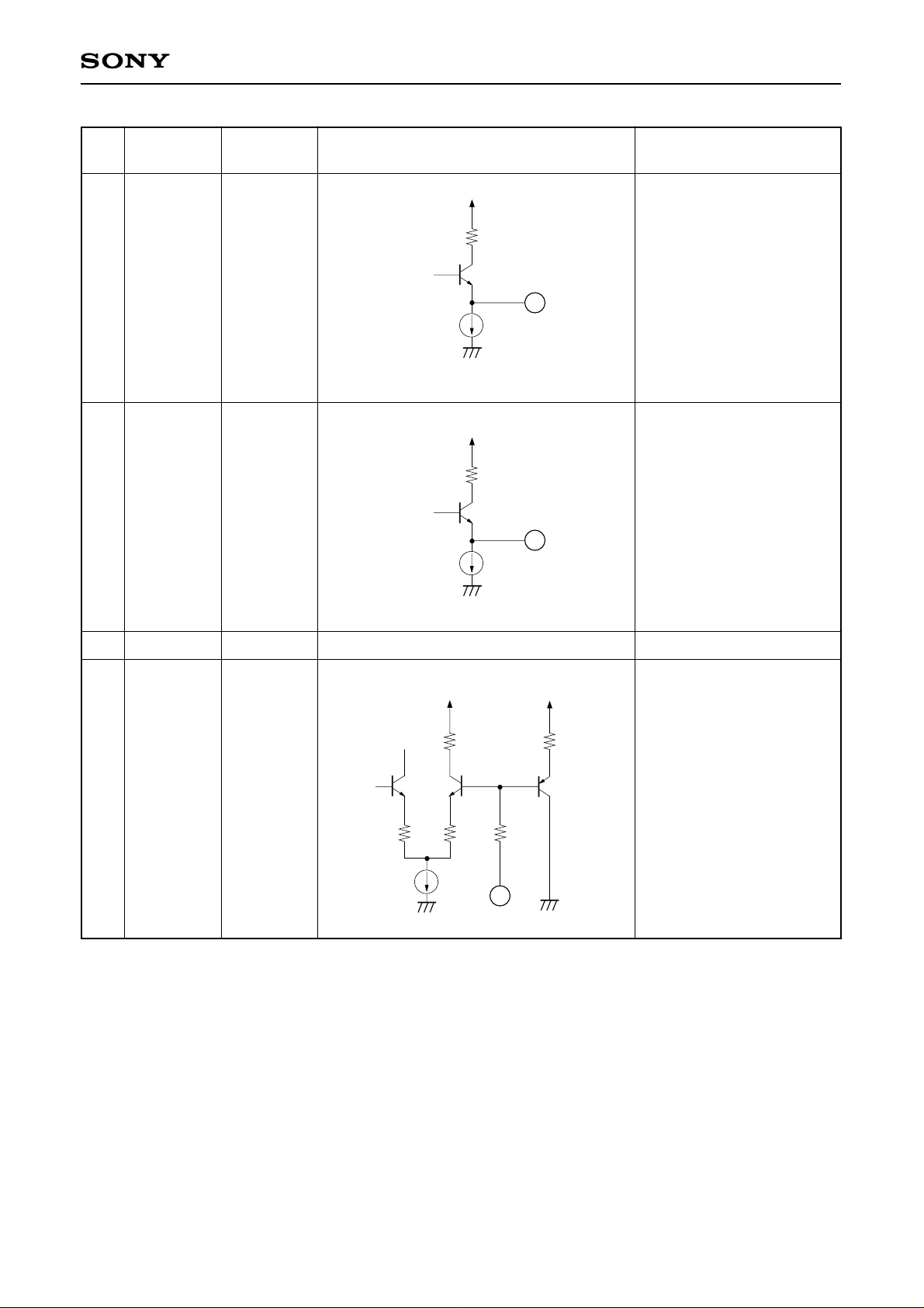
24
25
Symbol Pin voltage Equivalent circuit Description
431
CS signal output pin
CS OUT
YL OUT
1.5 to 1.8V
1.9 to 2.3V
200µA
431
80µA
25
24
Sig: Max. 1V
YL signal output pin
26 GND1
C-γ CONT
27
0V: Typ.
γ curve
30k
40µA
1k
30k
GND
100k
Chroma (R.G.B)
γ curve adjustment pin
147
27
– 7 –
Page 8
CXA1391Q/R
PIn
No.
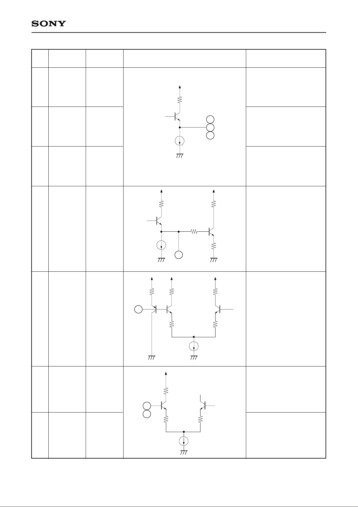
28
29
30
31
Symbol Pin voltage Equivalent circuit Description
R signal output pin
WB Mode:
WB R
1.4 to 2V
Sig: Typ. 400mV
γ Mode:
431
Sig: Typ. 500mV
G signal output pin
WB G
1.4 to 2V
28
29
30
200µA
WB Mode:
Sig: Typ. 400mV
γ Mode:
Sig: Typ. 500mV
B signal output pin
WB Mode:
WB B
1.4 to 2V
Sig: Typ. 400mV
γ Mode:
Sig: Typ. 500mV
431 1k
When used as output pin,
it is an Auto WB DC output
pin.
Pin 28, 29 and 30 turn
to WB mode.
WB DC
1.4 to 2V
300
32
C SLICE
33
C LEVEL
47 C1 GAIN
0V:
Slice OFF
1.8 to 5V
(Control)
1.8 to 5V
(Control)
100k
32
200µA
33
47
30k
18k
1k
31
1k
40µA
67µA
30k
100k
18k
When connected to Vcc:
Pins 28, 29 and 30 turn to
γ mode.
Chroma (R.G.B) signals
dark slice level adjustment
pin
Chroma (R.G.B) gain
control pin
(Chroma modulation factor
control for all 3 channels)
DL C1 signal gain control
pin
(1H delay line gain
compensation)
– 8 –
Page 9
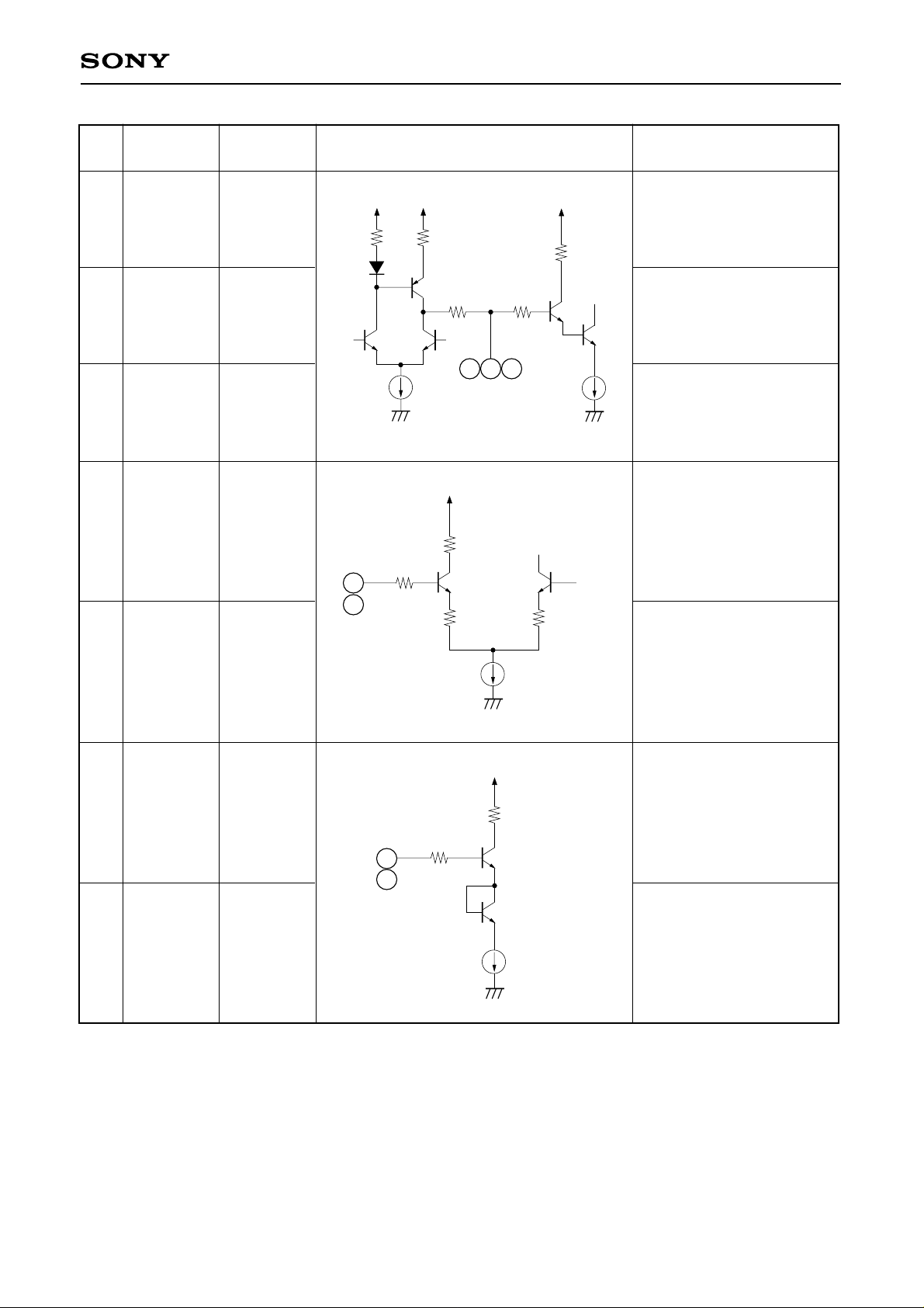
CXA1391Q/R
PIn
No.
34
35
36
37
Symbol Pin voltage Equivalent circuit Description
Capacitor connecting pin
CLP C R
CLP C G
3.0 to 3.6V
3.0 to 3.6V
2.2k 2.2k
1k
147
for R WB amplifier clamp
(Clamp at CLP2)
1k
Capacitor connecting pin
for G WB amplifier clamp
(Clamp at CLP2)
35
36
34
CLP C B
125µA
3.0 to 3.6V
40µA
Capacitor connecting pin
for B WB amplifier clamp
(Clamp at CLP2)
Rch WB amplifier gain
control pin
(Pre-WB)
R GAIN
1.8 to 5V
(Control)
37
40
147
15k
1k
15k
40
38
39
B GAIN
R CONT
B CONT
1.8 to 5V
(Control)
2.5 to 4.6V
2.5 to 4.6V
38
39
147
80µA
1k
10µA
Bch WB amplifier gain
control pin
(Pre-WB)
Rch WB amplifier gain
control pin
Bch WB amplifier gain
control pin
– 9 –
Page 10
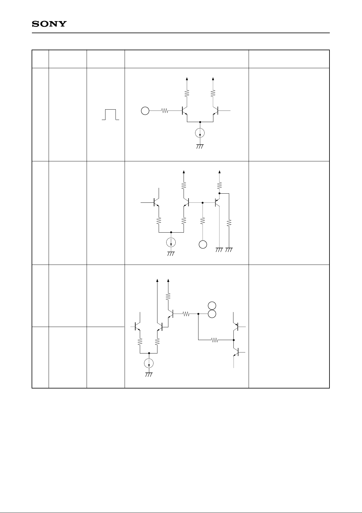
CXA1391Q/R
PIn
No.
41
42
Symbol Pin voltage Equivalent circuit Description
ID pulse
(color discrimination pulse)
input pin
(CMOS level VIH = 2.5V)
ID = L C0 → CR
ID
5V
0
41
147
1k
30k
C1 → CB
40µA
ID = H C0 → CB
C1 → CR
B MTX
1.8 to 5V
(Control)
0V
(Preset)
15k
1k
15k 147
100k
100k
B signal operations MTX
coefficient adjustment pin
(Coefficient 0.22)
Refer to Note 2.
43
44
CLP C
MPX2
CLP C
MPX1
2.7 to 3.1V
2.7 to 3.1V
6k
6k
40µA
1k
80µA
147
42
43
44
147
Capacitor connecting pin
for MPX clamp
(Clamp at CLP2)
– 10 –
Page 11
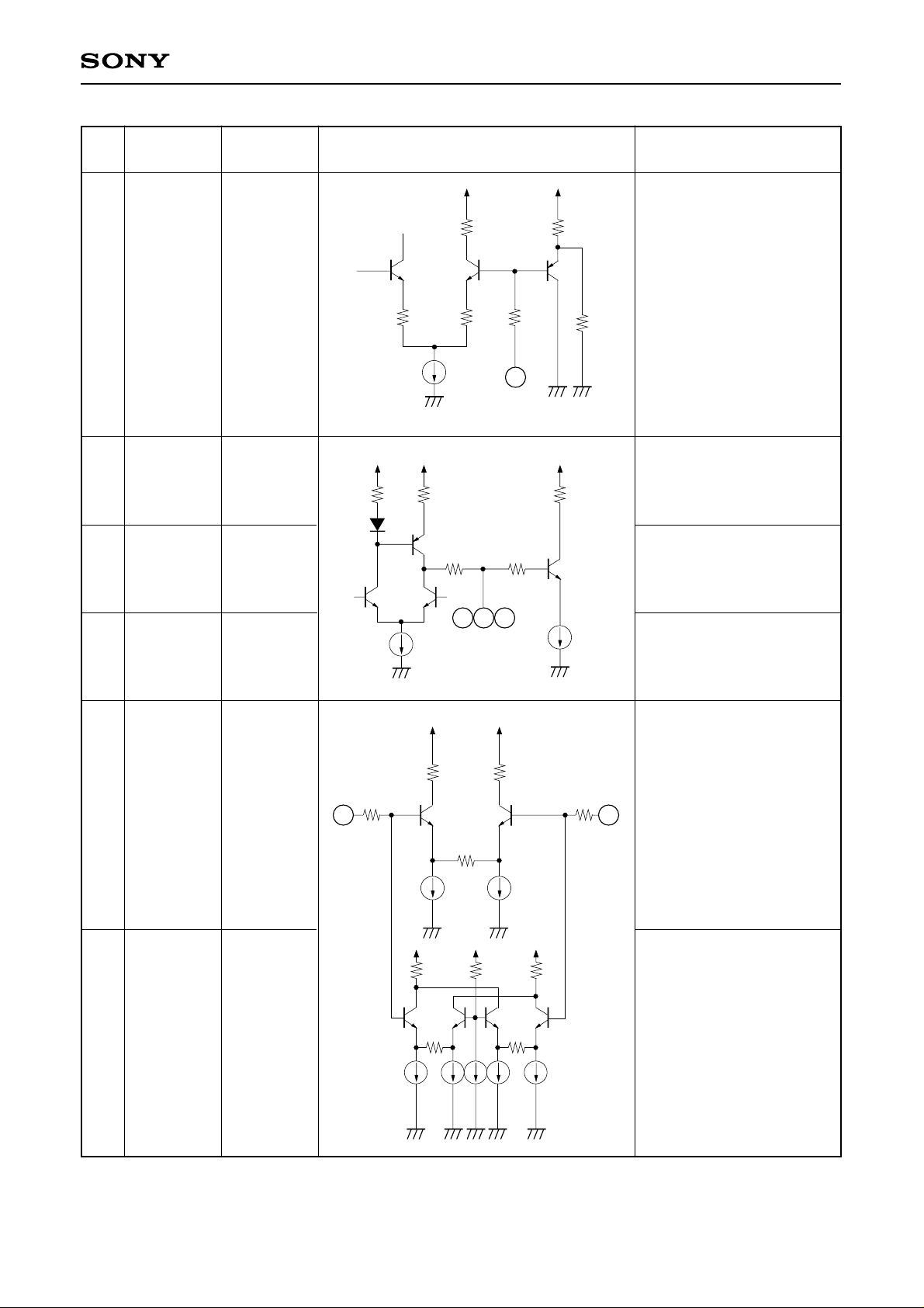
CXA1391Q/R
PIn
No.
45
48
55
Symbol Pin voltage Equivalent circuit Description
R MTX
DLC1 IN
DLY1 IN
1.8 to 5V
(Control)
0V
(Preset)
C-Couple
input
3.1 to 3.5V
C-Couple
input
3.6 to 4.0V
30k
2.6k 2.6k
1k
300k 147
40µA
1k 147
45
100k
1k
100k
R signal operations MTX
coefficient adjustment pin
(Coefficient 0.617)
Refer to Note 2.
DL C1 signal input pin
Sig: Typ. 150mVp-p
(Negative polarity)
DL Y1 signal input pin
Sig: Typ. 150mVp-p
(Negative polarity)
56
49
50
DLY2 IN
S2 IN
S1 IN
C-Couple
input
3.6 to 4.0V
1.9V
1.9V
55
48
56
150µA
147 147
49
7.5k
40µA 40µA
11µA
DL Y2 signal input pin
Sig: Typ. 150mVp-p
(Negative polarity)
S2 signal input pin
50
Sig: Typ. 500mV
Max. 1500mV
S1 signal input pin
Sig: Typ. 500mV
Max. 1500mV
40µA
40µA
40µA
40µA
40µA
– 11 –
Page 12

CXA1391Q/R
PIn
No.
51
57
Symbol Pin voltage Equivalent circuit Description
2.6k1k
147 1k
Capacitor connecting pin
CLP C Y0
3.3 to 3.7V
for Y0 clamp
(Clamp at CLP4)
51
40µA 150µA
1k
DL Y2 signal gain control
pin
(1H delay line gain
compensation)
V-APCON mode selection
0V: 2H Mode
Y2 GAIN
1.8 to 5V
(3H Mode)
0V
(2H Mode)
147
57
15k
1.8 to 5V: 3H Mode
58
59
60
GND2
LPF Adj. 1
LPF Adj. 2
1.8 to 2.2V
1.8 to 2.2V
59
60
300
5k
80µA
10µA
20k
GND
Connecting pin of the
external resistor that
determines the
characteristics of the LPF
for 1H DL.
(External resistor in the
range of 15 to 27kΩ)
Connecting pin of the
external resistor that
determines the
characteristics of the
chroma LPF
(LPF for R, G, B, CS).
(External resistor in the
range of 15 to 62kΩ)
– 12 –
Page 13
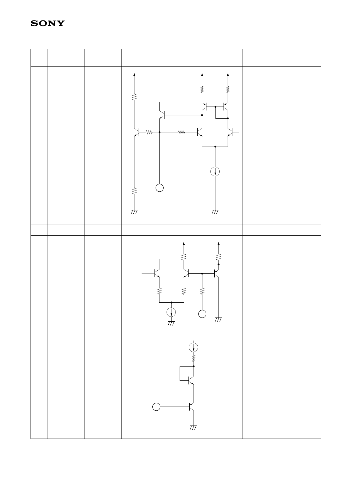
CXA1391Q/R
PIn
No.
61
Symbol Pin voltage Equivalent circuit Description
1k
Connecting pin of the
external resistor that
300300
determines the
characteristics of the LPF
LPF Adj. 3
1.8 to 2.2V
for V-APCN.
(External resistor in the
range of 15 to 62kΩ)
When connected to Vcc,
10µA
the LPF for V-APCN turns
OFF.
120k
61
62 Vcc
0V
(Typ. γ curve)
Y-γ CONT
63
1.8 to 5V
(Control)
64 YH IN 0.95V
30k
1k
30k 147
40µA
Power supply 5V (Typ.)
100k
YH γ curve adjustment
63
10k
YH signal input
Sig: Typ. 220mV
Max. 660mV
64
– 13 –
Page 14

Electrical Characteristics
CXA1391Q/R
Item
Current consumption
S2–S1 Amp Gain
DLC1
Max.
gain control
Min.
S1+S2 Amp
Gch Y
Chroma matrix
(Gch)
Note 3)
CR/Y
–CB/Y
Rch CR
Chroma matrix
(Rch)
Note 3)
Y
(Preset)
Y (Max.)
Y (Min.)
Bch–CB
Chroma matrix
(Bch)
Note 3)
Y
(Preset)
Y (Max.)
Y (Min.)
Symbol Conditions Min. Typ. Max. Unit
ID
SSG
Input: S1 IN = –62.5mV, S2 IN = 62.5mV
Calculations: DLC0 OUT/S1 IN
25
–3
34.5
–1.95
43
–1
mA
dB
Input: DLC1IN = 100mV
DLC1H
Conditions: C1Gain = 5V
C-level = 5V
6
7
9
dB
Calculations: (WB-R/DLC1IN) –CG Note2)
DLC1L
SAG
Conditions: C1Gain = 0V
(Others same as DLC1H)
Input: S1 IN = 500mV
Calculations: DLY0OUT/S1 IN
–2
–15
–0.85
–14
0
–13
dB
dB
Input: S1 IN = S2 IN = 300mV
GY
Conditions: C-level = 5V
80
100
120
mV
Calculations: WB-G (ID = H, L average)
Input: S1 IN = S2 IN = 62.5mV
GCR
Conditions: C-level = 5V
0.9
1
1.1
—
Calculations: WB-G/GY (ID = L)
GCB
ID = H (Others same as GCR)
–1.1
–1
–0.9
—
Input: S1 IN = –62.5mV, S2 IN = 62.5mV
RCR
Conditions: C-level = 5V
70
85
100
mV
Calculations: WB-R (ID = L)
Input: S1 IN = S2 IN = 500mV
RYP
Conditions: C-level = 5V
0.15
0.168
0.186
—
Calculations: WB-R/RCR (ID = H)
RYH
RYL
RMTX = 5V (Others same as RYP)
RMTX = 1.8V (Others same as RYP)
0.22
0.11
0.25
0.125
0.27
0.14
—
—
Input: S1 IN = 62.5mV, S2 IN = –62.5mV
BCB
Conditions: C-level = 5V
80
100
120
mV
Calculations: WB-B (ID = H)
Input: S1 IN = S2 IN = 500mV
BYP
Conditions: C-level = 5V
0.2
0.22
0.24
—
Calculations: WB-B/BCB (ID = H)
BYH
BYL
BMTX = 5V (Others same as BYP)
BMTX =1.8V (Others same as BYP)
0.31
0.13
0.34
0.15
0.37
0.17
—
—
– 14 –
Page 15
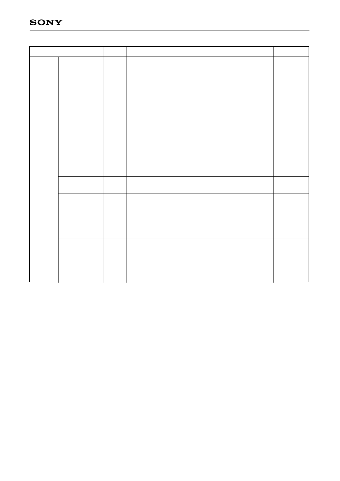
CXA1391Q/R
Item Symbol Conditions Min. Typ. Max. Unit
Input: DLC1IN = –200mV
Conditions: C-level = 5V
RCONT = 4.6V (ID = H)
RCONT Max.
RCH
Calculations: WB-R/WB-RTyp. Note 4)
7.5
8.2
8.5
dB
WB-R Typ. is the tested output of WB-R
when RCONT is set to 4V (Other inputs,
conditions same as RCH)
WB
GAIN
RCONT Min.
BCONT Max.
BCONT Min.
RGAIN Max.
BGAIN Max.
RCL
BCH
BCL
RGH
BGH
Test: RCONT = 2.5V
(Others same as RCH)
Input: DLC1IN = 150mV
Conditions: C-level = 5V
BCONT = 4.6V (ID = L)
Calculations: WB-B/WB-BTyp. Note 4)
WB-B Typ. is the tested output of WB-B
when BCONT is set to 4V (Other inputs,
conditions same as BCH)
Test: BCONT = 2.5V
(Others same as BCH)
Input: DLC1IN = –200mV
Conditions: RCONT = 2.5V RGAIN = 5V
C-level = 5V (ID = H)
Calculations: WB-R/WB-RMin.
WB-R Min. is the tested WB-R, when
tested under the same conditions as RCL.
Input: DLC1IN = 150mV
Conditions: BCONT = 2.5V BGAIN = 5V
C-level = 5V (ID = L)
Calculations: WB-B/WB-BMin.
WB-B Min. is the tested WB-B, when
tested under the same conditions as BCL.
–8.4
7.5
–8.4
8.6
11.4
–7.9
8.2
–7.9
9.2
12.2
–7.4
8.5
–7.4
—
—
dB
dB
dB
dB
dB
– 15 –
Page 16
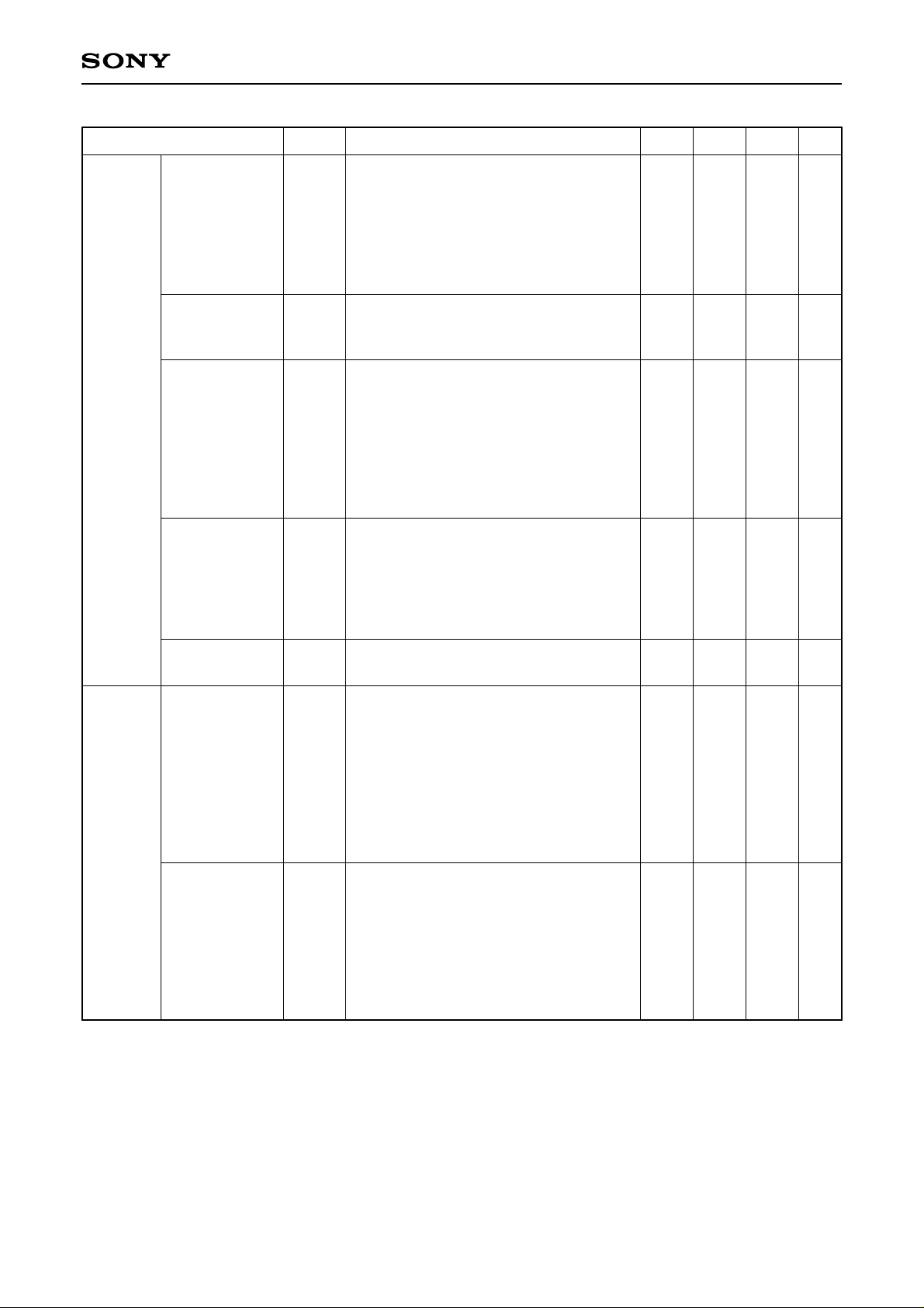
CXA1391Q/R
Item Symbol Conditions Min. Typ. Max. Unit
Input: S1IN = 200mV S2IN = 160mV
DLC1IN = 220mV
R–G OUT/
WB-B
BMBY
Conditions: C-γ CONT = WB DC =
C-Slice = C-level = 5V
RCONT = 2.5V
0.4
0.44
0.48
—
BCONT = 4.6V (ID = L)
Calculations: B–Y OUT/WB-B
Bch
color
difference
matrix
Note 5)
Gch
color
difference
matrix
Note 5)
R–Y OUT/
WB-B
B–Y GAIN
Max.
B–Y Hue Max.
B–Y Hue Min.
R–Y/R–G
B–Y/B–G
BMRY
BMG
BMHH
BMHL
GMR
GMB
Conditions: R–Y GAIN = 1.8V
Calculations: R–Y OUT/WB-B
(Others same as BMBY)
Conditions: BCONT = 4V
1. B–Y OUT is tested when B–Y
gain = 0V and taken as A. (Other
conditions are the same as BMBY)
2. B–Y OUT is tested when B–Y
gain = 5V and taken as B. (Other
conditions are the same as BMBY)
Calculations: B/A
Conditions: B–Y HUE = 1.8V
(Others same as BMBY)
Calculations: R–Y OUT/B–Y Typ.
B–Y Typ. is the value of the tested B–Y
OUT when B–Y hue=0V (Other conditions
are the same as BMBY). Note 6)
B–Y HUE = 5V
(Others same as BMHH)
Input: S1IN = 830mV S2IN = 660mV
DLC1IN = –230mV
Conditions: WB-DC = C-level = 5V
RCONT = BCONT = 2.5V
1. R–Y OUT is tested when R–Y
gain = 0V and taken as A.
2. R–Y OUT is tested when R–Y
gain = 1.8V and taken as B.
Calculations: B/A
Input: (The same as GMR)
Conditions:
1. B–Y OUT is tested when B–Y
gain = 0V and taken as A.
2. B–Y OUT is tested when R–Y
gain = 1.8V and taken as B.
(Others same as GMR)
Calculations: B/A
–0.24
3.0
0.58
—
0.81
0.63
–0.21
3.3
0.68
–0.67
0.85
0.66
–0.17
—
—
–0.58
0.89
0.7
—
—
—
—
—
—
– 16 –
Page 17
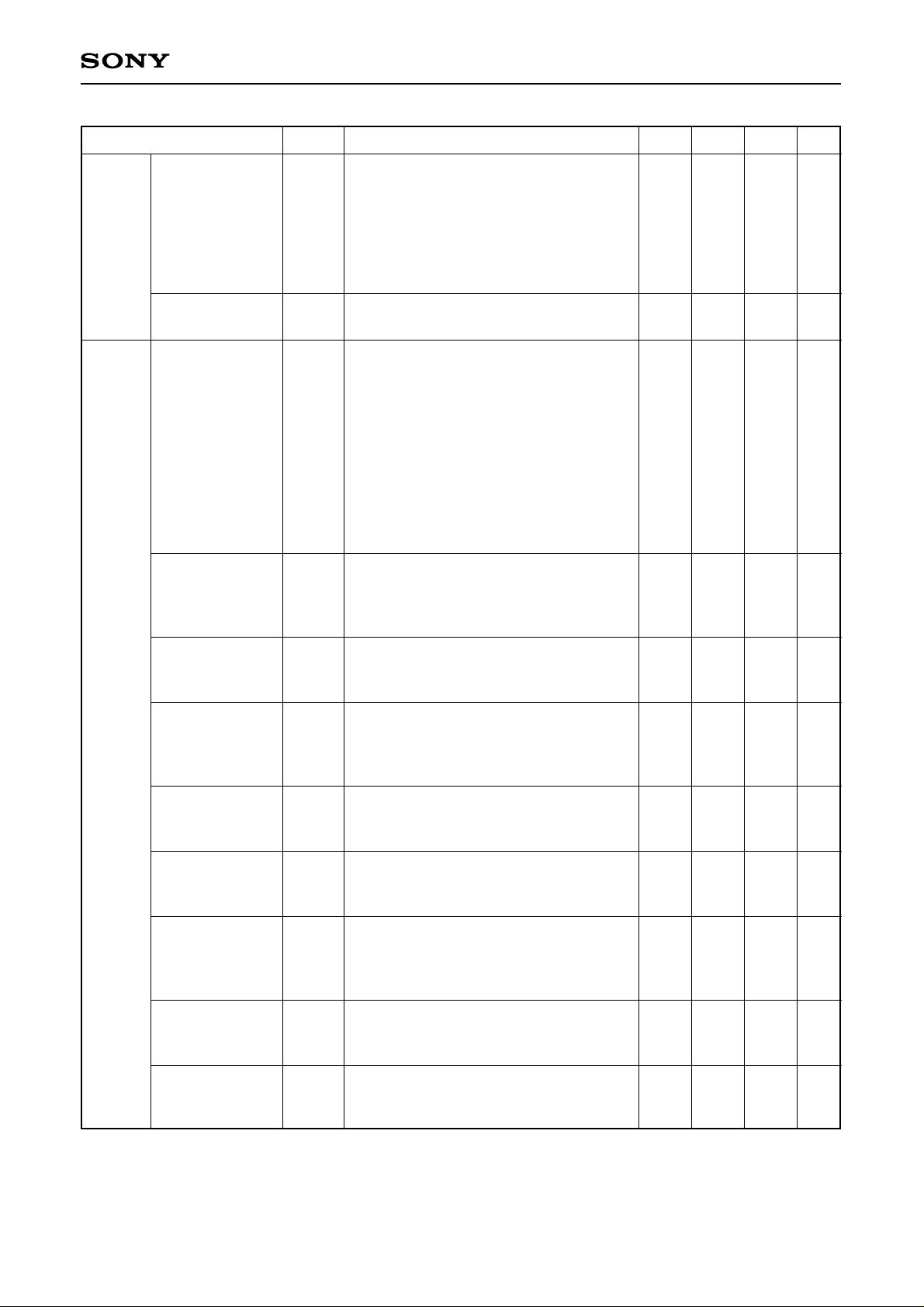
C-Slice
CXA1391Q/R
Item Symbol Conditions Min. Typ. Max. Unit
Input: DLY1IN = –400mV
Conditions: C-level = 5V
Y1GAIN = 1.8V
Typ.–Min.
CSLL
C-Slice = 1.8V (ID = H)
0
5
15
Calculations: C-Slice Typ. -TP
C-Slice Typ. is the TP output of
C-Slice = 0V.
mV
Gch γ
curve
Typ.–Max.
C-γ CONT=0V
Gch-WB=400mV
C-γ CONT=0V
Gch-WB=800mV
C-γ CONT=0V
Gch-WB=100mV
C-γ CONT=1.8V
Gch-WB=400mV
CSLH
γTyp.
γL8
γL1
γM4
Conditions: C-Slice =5V
(Others same as CSLL)
Input: DLY1IN = –200mV
S1IN = S2IN = 500mV
Conditions: Y1GAIN = 1.8V
C-level is valied and
adjusted to obtain 400mV at
WB-G.
After that C-level is fixed
during test.
WB-DC is set to OPEN during C-level
adjusted and set to 5V during test.
Calculations: WB-G is tested.
Input: DLY1IN = –400mV
S1IN = S2IN = 1000mV
Conditions: Same as γ Typ.
Calculations: WB-G/γ Typ.
Input: DLY1IN = –50mV
S1IN = S2IN = 125mV
(Others same as γL8)
Input: DLY1IN = –200mV
S1IN = S2IN = 500mV
Conditions: Cγ CONT = 1.8V
Calculations: WB-G/γ Typ.
95
450
1.13
0.36
0.9
120
500
1.2
0.4
1
145
550
1.25
0.44
1.1
mV
mV
—
—
—
C-γ CONT=1.8V
Gch-WB=800mV
C-γ CONT=1.8V
Gch-WB=100mV
C-γ CONT=5V
Gch-WB=400mV
C-γ CONT=5V
Gch-WB=800mV
C-γ CONT=5V
Gch-WB=100mV
γM8
γM1
γH4
γH8
γH1
Input: DLY1IN = –400mV
S1IN = S2IN = 1000mV
(Others same as γM4)
Input: DLY1IN = –50mV
S1IN = S2IN = 125mV
(Others same as γM4)
Input: DLY1IN = –200mV
S1IN = S2IN = 500mV
Conditions: Cγ CONT = 1.8V
Calculations: WB-G/γ Typ.
Input: DLY1IN = –400mV
S1IN = S2IN = 1000mV
(Others same as γH4)
Input: DLY1IN = –50mV
S1IN = S2IN = 125mV
(Others same as γH4)
– 17 –
1.13
0.45
0.9
1.13
0.26
1.2
0.5
1
1.2
0.3
1.25
0.55
1.1
1.25
0.35
—
—
—
—
—
Page 18
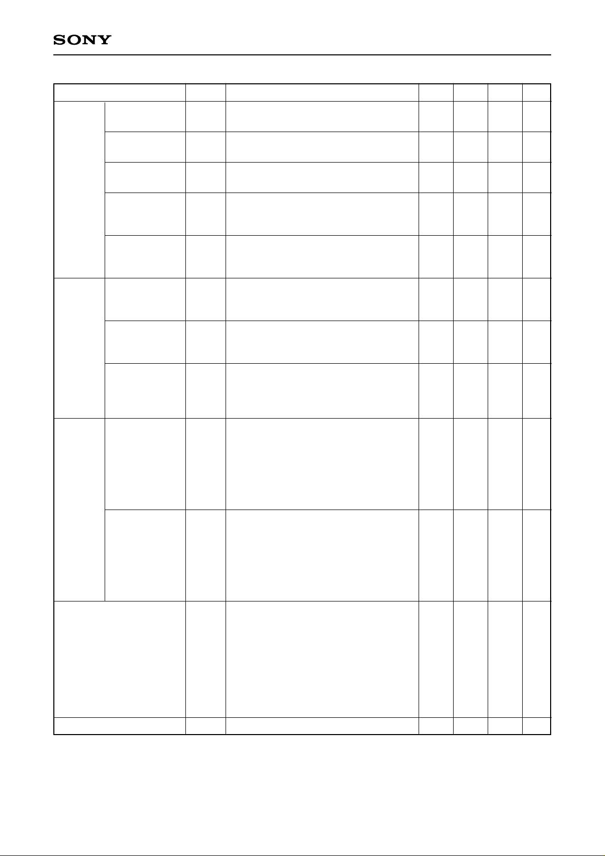
CXA1391Q/R
Item Symbol Conditions Min. Typ. Max. Unit
Yγ
TP
Yγ1.0 (Typ.)
Yγ2.0/Yγ1.0
Yγ0.5/Yγ1.0
Yγ0.5 (Max.)/
Yγ1.0
Yγ0.5 (Min.)/
Yγ1.0
TP (YH)
TP (DLYH)
TP (GWBS)
YγT
Yγ2.0
Yγ0.5
YγH
YγL
TPY
TPDY
TPG
Input: YHIN = 220mV
Calculations: DLYHOUT
Input: YHIN = 440mV
Calculations: DLYHOUT/YγT
Input: YHIN = 110mV
Calculations: DLYHOUT/YγT
Input: YHIN = 110mV
Conditions: Yγ CONT = 1.8V
Calculations: DLYHOUT/YγT
Input: YHIN = 110mV
Conditions: Yγ CONT = 5V
Calculations: DLYHOUT/YγT
Input: YHIN = 220mV
Conditions: DLYHGAIN = 1.8V
Calculations: TP/DLYHOUT
Input: DLYHIN = YγT × 0.7
Conditions: Same as TPY
Calculations: TP/–DLYHOUT Note 7)
Input: S1IN = S2IN = 500mV
DLY1IN = 200mV
Conditions: Y1GAIN = 1.8V
Calculations: TP/WB-G
–440
1.23
0.59
0.64
0.54
–5
–5
–2
–400
1.37
0.66
0.71
0.6
–4
–4
0
–360
1.51
0.73
0.78
0.66
–3
–3
2
mV
—
—
—
—
dB
dB
dB
Min. Gain
YH AMP
Max. Gain
Chroma level Max./Min.
YLG
YHG
GCL
Input: YHIN = 220mV
DLYHIN = – [YγT × –3.5dB]
Conditions: DLYHGAIN = 1.8V
Calculations: TP is tested to check that
the signal level is below
0mV in relation to black
level. Note 8)
Input: YHIN = 220mV
DLYHIN = – [YγT × –12dB]
Conditions: DLYHGAIN = 5V
Calculations: TPTP is tested to check that
the signal level is over
0mV in relation to black
level. Note 8)
Input: DLC1IN = 200mV
Conditions:
1. WB-G is tested when C-level = 5V
and taken as GC-level Min.
2. WB-G is tested when C-level = 1.8V
and taken as GC-level Max.
(Both 1 and 2 test at ID-H.)
Calculations: GC-level Max. /
GC-level Min.
—
12
1.55
—
—
1.65
3.5
—
1.75
dB
dB
—
WB DC
WDDC
Test: WB-DC
– 18 –
1.4
1.6
2
V
Page 19
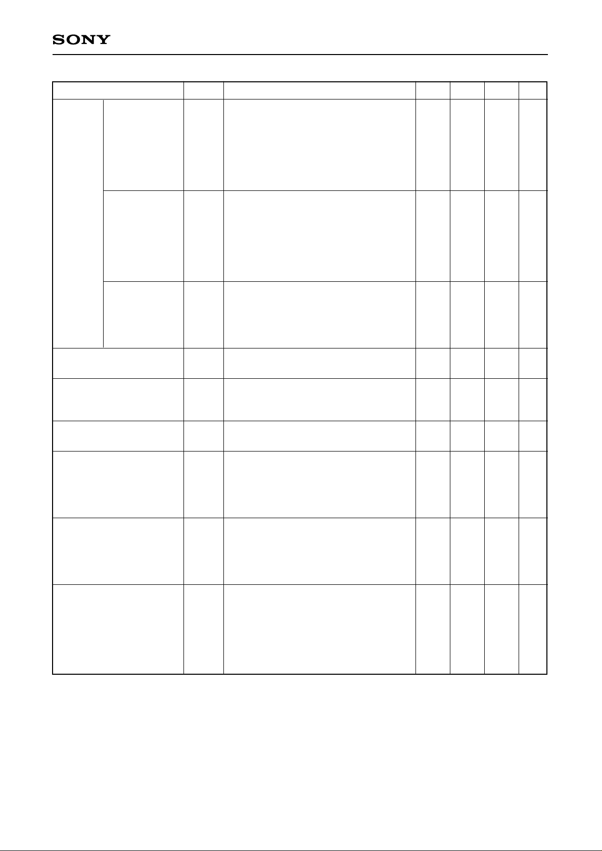
CXA1391Q/R
Item Symbol Conditions Min. Typ. Max. Unit
Input: S1IN = 150mV S2IN = 450mV
Conditions: C-γ CONT = WB
YLOUT/
RγOUT
YLR
DC = C-Slice =
C-level = 5V
RCONT = 4.6V BCONT = 2.5V
0.27
0.3
0.34
—
BGAIN = 1.8V (ID = L)
Calculations: YLOUT/WB-R
YL
Note 5)
YLOUT/
BγOUT
YLOUT/
GγOUT
YHOUT1 (OH mode)
YHOUT1 1H/0H
YHOUT2 (0H) /YHOUT1
YHOUT2 (1H) /YHOUT1
YLB
YLG
YH1Z
YH1O
YH2Z
YH2O
Input: S1IN = 200mV S2IN = 160mV
DLC1IN = 220mV
Conditions: C-γ CONT = WB
DC = C-Slice =
C-level = 5V RCONT = 2.5V
BCONT = 4.6V (ID = L)
Calculations: YLOUT/WB-B
Input: S1IN = 830mV S2IN = 660mV
DLC1IN = –230mV
Conditions: WB-DC = C-level = 5V
RCONT = BCONT = 2.5V
Calculations: YLOUT/WB-G
Input: YHIN = 220mV
Calculations: YHOUT1 is tested.
Input: DLYHIN = – (YγT × –4dB)
Conditions: DLYHGAIN = 1.8V
Calculations: YHOUT1/YH1Z Note 8)
Input: YHIN = 220mV
Calculations: YHOUT2/YH1Z
Input: YHIN = 220mV
Conditions: DLYHGAIN = 1.8V
Calculations: YHOUT2/YHOUT2Typ.
YHOUT2Typ. is YHOUT2 output tested at
YH2Z.
0.08
0.54
900
–1
–1
–6.5
0.1
0.6
1000
0
0
–6
0.12
0.66
1100
1
1
–5.5
—
—
mV
dB
dB
dB
VAP Typ.
Note 9)
VAP Slice
Note 9)
VAPT
VS
Input: S1IN = S2IN = 125mV
Conditions: VAP GAIN = 1.8V
VAP Slice = 1.8V
Y2 GAIN = 1.8V
Calculations: VAP OUT is tested.
Input: S1IN = S2IN = 1000mV
Conditions: Y2 GAIN = 1.8V
1. VAP OUT is tested when VAP
Slice=1.8V and taken as SMin.
2. VAP OUT is tested when VAP
Slice=5V and taken as SMax.
Calculations: SMax.–SMin. Note 10)
– 19 –
–250
256
–200
320
–150
384
mV
mV
Page 20

DLY1
gain
Note 11)
DLY2
gain
CXA1391Q/R
Item Symbol Conditions Min. Typ. Max. Unit
Input: S1IN = S2IN = 500mV
DLY1IN = –200mV
Conditions: VAP GAIN = VAP
Min.
DY1L
Calculations: VAP-OUT is tested to check
Slice = Y1GAIN = 1.8V
—
—
0
dB
that the signal level is over
0mV in relation to black
level.
Input: S1IN = S2IN = 500mV
DLY1IN = –110mV
Conditions: VAP GAIN = VAP Slice =
1.8V
Max.
DY1H
Y1GAIN = 5V
5
—
—
dB
Calculations: VAP-OUT is tested to check
that the signal level is below
0mV in relation to black
level.
Input: S1IN = S2IN = –167mV
DLY2IN = –66.7mV
Conditions: VAP GAIN = VAP
Min.
DY2L
Slice = Y1GAIN = Y2GAIN = 1.8V
—
—
0
dB
Calculations: VAP-OUT is tested to check
that the signal level is over
0mV in relation to black
level.
Note 11)
CS
Note 12)
Max.
VCS Typ.
VCS Min.
VCS Max.
VCS Typ.
DY2H
VCST
VCSL
VCSH
CST
Input: S1IN = S2IN = –167mV
DLY2IN = –37.5mV
Conditions: Y2GAIN = 5V
(Others same as DY2L)
Calculations: VAP-OUT is tested to check
that the signal level is below
0mV in relation to black
level.
Input: S1IN = S2IN = 167mV
Conditions: Y1GAIN = Y2GAIN = 1.8V
CS GAIN = 5V
Calculations: CS OUT is tested.
Conditions: CS GAIN = 0V
(Others same as VCST)
Calculations: CS OUT/VCST
Conditions: CS GAIN = 1.8V
(Others same as VCSL)
Input: CS-IN = 500mV
5
90
—
4.4
440
—
120
0
465
—
150
0.05
—
490
dB
mV
—
—
mV
– 20 –
Page 21
CXA1391Q/R
Note 1) For pins without specific instructions regarding input, feed the DC value shown on the Test Circuit.
Calculations are mentioned utilizing the pin name or the electrical characteristics symbols. Otherwise,
for exceptional notations explanatory notes, are given with every case.
Note 2) In this item, the gain of DLC1 amplifier exclusively is calculated. CG is the gain of the system from
DLC1 IN to WB-R from which DLC1 GC amplifier gain has been excluded.
—CG calculating method—
In the actual calculation, the system on C0 side is utilized.
Input: S1IN = –62.5mV S2IN = 62.5mV
Condition: Same as DLC1H
Calculations: CG = 20log (WB-R/DLC0OUT)
Note 3) Chroma matrix operations
R = 2 [CR + αY] α: Control with RMTX (Preset 0.167)
G = Y – (CR + CB)
B = 2 [CB + ß (Y – C)] ß: Control with BMTX (Preset 0.22)
Note 4) With the typical gain taken when R CONT is at 4V, compare with the gain during Max. and Min. The
same for B CONT.
Note 5) Adjustment and testing is performed so that signals are output only for each of R, G, B channels
respectively.
Note 6) Comparison with B–Y OUT when R–Y HUE = 0V (HUE OFF).
The same for B–Y HUE.
Note 7) The compensation of difference in gain of YH0 andYH1 is as follows.
1) At DLYH GAIN = 1.8V, DLYH amplifier gain is 3dB.
2) Test DLYH OUT (tested at YrT) when YH IN = 220mV signal is input.
3) The difference in gain between YH0 and YH1 is compensated by inputting the signal as –3dB to
DLYH IN.
Note 8) The amplifier input is varied and the gain confirmed.
Note 9) VAP (Vertical Aperture Compensation)
Note 10) Dark slice variable volume. (Output level difference between the value slice volume at Max. and slice
volume at Min.)
Note 11) Utilizing V-APCN 2H mode, DLY1 amplifier exclusive gain is obtained through operations. However,
as the amplifier gain cannot be tested directly, only the upper and lower limits of the gain control are
checked according to the following method.
(a) Lower limit check
S1 IN = S2 IN = 500mV (At that time KNEE circuit input turns to 200mV)
DLY1 IN = –200mV (For others refer to the conditions chart)
In this condition, if we have VAP OUT ≥ 0, this indicates that DLY1 amplifier is below 0dB.
(b) Upper limit check
S1 IN = S2 IN = 500mV
DLY1 IN = –110mV (in (a) the –5dB of –200mV)
In this condition, if we have VAP OUT ≤ 0, this indicates that DLY1 amplifier is above 5dB.
Note 12) CS (Chroma Suppress)
– 21 –
Page 22
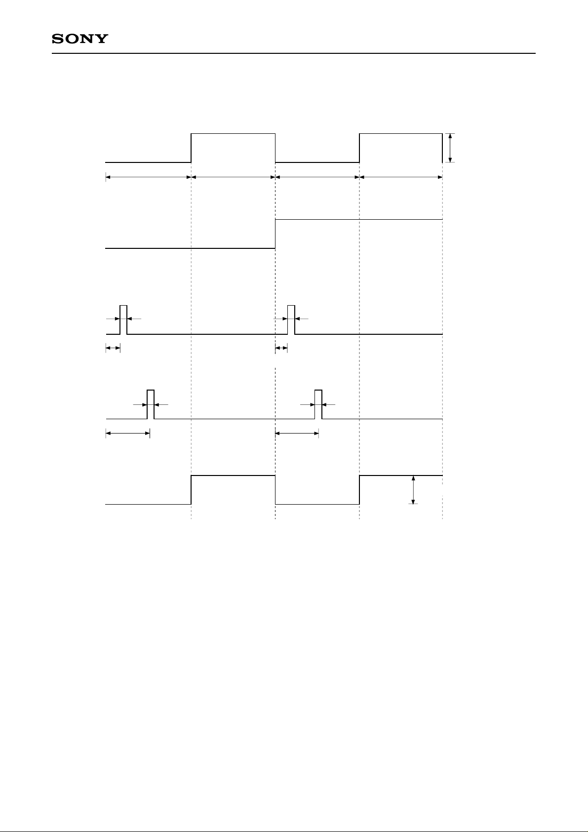
Timing Chart for Testing
CXA1391Q/R
Input waveform
5V
t
D
0V
5V
CLP2
0V
5V
CLP4
0V
5µ
30µ 30µ 30µ 30µ
2µ2µ
5µ
2µ 2µ
Differs with each test
D
LYH IN
CS IN
DLC1 IN
S1
S2
DLY1 IN
DLY2 IN
YH IN
Output waveform
15µ
DLY
H OUT
YH OUT1
YH OUT2
TP
VAP_OUT
B – Y OUT
R – Y OUT
CS OUT
YL OUT
WB_R
15µ
Output signal
WB_G
WB_B
DLC0 OUT
DLY0 OUT
DLY1 OUT
– 22 –
Page 23

CXA1391Q/R
0V
5V
V
V
C SLICE
WB DC
WB B
WB G
31
32
33
C LEVEL
34
CLF C R
CLP
35
CLP C G
36
CLP C B
37
R GAIN
38
R CONT
39
B CONT
40
B GAIN
41
ID
0V 0V 4V 0V 0.1V 0V0.1V0.1V4VID0.1
V
V
0V 0V 0.1
0.1
42
B MTX
43
CLP C MPX2
44
CLP C MPX1
45
R MTX
46
DLCO OUT
47
C1 GAIN
48
DLC1 IN
(CLP2)
LPF
WB AMP
BGR
WB CONTROL
MATRIX
Y
CR
-CB
&
CLP
MPX
(CLP2)
C1
C0
LPF
LPF
CLP
GC
LPF
C0
S2 IN
Y0
49
50
S1 IN
29
30
B-r
B-WB
G-WB
R-WB
Y1
Y0
(CLP4)
LPF
(CLP4)
Y0
CLP
LPF
51
52
CLP C YO
DLY0 OUT
0.1
0V
WB R
C-r CONT
GND 1
YL OUT
28
27
R-r
G-r
SLICE
25
26
B-r
r
G-r
R-r
MAX
Y0
Y1
Y2
LPF
LPF
Y1
Y2
CLP
CLP
(CLP4)
(CLP4)
GC
GC
54
53
Y1 GAIN
DLY1 OUT
DLY1 IN
56
55
DLY2 IN
0.1
0.1
CS OUT
YL MTX
CS VAP
GC
ABS
Y2 GAIN
0V
0V
0V
CS GAIN
R-Y HUE
B-Y HUE
R-Y OUT
24
23
21
22
20
0V
0V
B-Y OUT
B-Y GAIN
R-Y GAIN
19
17
18
0.1
16
CS IN
Hue & GC
R-Y
B-Y
MTX
R-Y
B-Y
(CLP4)
CLP
LPF
CS-Y
CS
CLP
SLICE
CS-Y
V-APCN
V-APCN
(CLP4)
CLP
KNEE
2H
APCN
–
KNEE
–
KNEE
3H
APCN
–
G ch SLICE
LPF
YH0
YH1
GC
V-APCN
CLP
(CLP4)
YH1
LPF ADJ 2
62k
61
60
LPF ADJ 3
62k
63
62
CC
V
Y-r CONT
10
57
58
59
GND 2
LPF ADJ 1
27k
YH IN
GC
15
14
13
12
11
10
9
8
7
6
5
4
YH0
3
r
2
1
CLP
(CLP2)
64
CLP C CS
VAP SLICE
CLP C VAP
0V 0V0.1 0.1
VAP GAIN
VAP OUT
CLP2
CLP4
CLP2
CLP4
0V
DLYH GAIN
TP
YH OUT 2
YH OUT 1
DLYH OUT
CLP C DLYH
3.65V
DC
DLYH IN
0.1 0.1
CLP C YH
Test Circuit (Typ. setting)
0V
DC 1.9V
DC 1.9V
0V
5V
5V
62k
0V
DC 0.95V
Note 1) µF is unit of capacitor
Note 2) indicates testing pin. (AC, DC test)
Note 3) Input pin DC value indicates input signal black level.
Note 4) indicate relay, side, normal close.
– 23 –
Page 24

Standard Control Characteristics (Vcc = 5V, Ta = 25°C)
C1 GAIN control characteristics R-MTX coefficient
3
GAIN converted into unit
2
CXA1391Q/R
0.3
GAIN
1
0.4
0.3
0.2
0.2
Preset
234 0
C1 GAIN voltage (V)
5
0.1
2345
R GAIN control characteristicsB-MTX coefficient
7
6
5
Preset
GAIN
4
3
R-MTX voltage (V)
0.1
0
2453
B-MTX voltage (V)
2
02 3 4 5
R GAIN voltage (V)
B GAIN control characteristics R/B CONT control characteristics
10
GAIN
8
6
4
2
2345
B GAIN voltage (V)
3
2
1/GAIN
1
2345
R/B CONT voltage (V)
– 24 –
Page 25

CXA1391Q/R
1.5
1
GAIN
0.5
3
2
C-SLICE control characteristics
245
3
C-LEVEL voltage (V)
R–Y/B–Y GAIN control characteristics
C-SLICE control characteristics
150
BLACK DC difference between sliced
signal and during sliced OFF
100
(mV)
50
0
C-SLICE power supply (V)
R–Y/B–Y HUE control characteristics
40°
30°
20°
10°
432
5
GAIN
1
3
2
GAIN
1
2345
R–Y/B–Y GAIN voltage (V)
Y1/Y2 GAIN control characteristics
–10°
–20°
–30°
(mV)
0°
R–Y/B–Y HUE voltage (V)
CS GAIN control characteristics
400
300
200
100
CS output during
S1 = S2 = 125mV input
(3H_Mode)
432
5
2345
Y1/Y2 GAIN voltage (V)
– 25 –
432
CS GAIN voltage (V)
5
Page 26

15
10
GAIN (dB)
5
CXA1391Q/R
DLYH GAIN control characteristics VAP control characteristics
400
VAP_OUT output
during S1 = S2 = 250mV input
(3H_Mode)
300
200
VAP OUT (mV)
100
300
200
(mV)
100
0
2345
DLY
H GAIN voltage (V)
VAP SLICE control characteristics
VAP GAIN = 0V
Diminution of VAP OUT
output level
2345
VAP SLICE voltage (V)
0
2345
VAP GAIN voltage (V)
– 26 –
Page 27
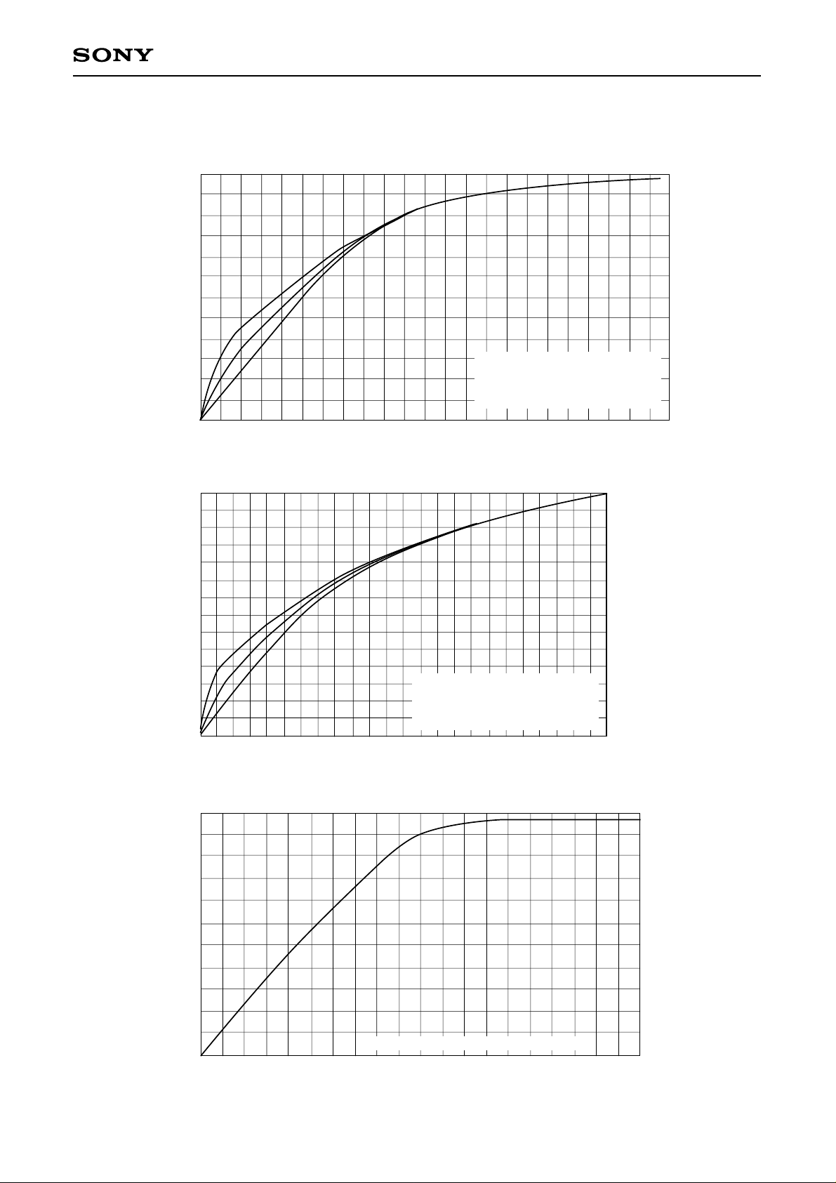
Standard Design Data
1.2
1.0
0.8
0.6
0.4
γ output (standardize)
0.2
CXA1391Q/R
Chroma γ curve (standardize)
1
2
3
Standardize at typical input (400mV)
1: C – γ CONT=1.6V (Max.)
2: C – γ CONT=0V (Typ.)
1: C – γ CONT=5V (Min.)
0.2 0.4 0.6 0.8 1.0 1.2 1.4 1.6 1.8 2.0 2.2
1.4
1.2
1.0
0.8
0.6
1
γ output (standardize)
0.4
0.2
2
3
0.2 0.4 0.6 0.8 1.0 1.2 1.4 1.6 1.8 2.0 2.2
γ input (standardize)
YH γ curve (standardize) (mV)
Standardize at typical input (220mV)
1: Y – γ CONT=1.6V (Max.)
2: Y – γ CONT=0V (Typ.)
1: Y – γ CONT=5V (Min.)
γ input (standardize)
V-APCN Knee (standardize) (mV)
1.0
0.8
0.6
0.4
Knee output (standardize)
0.2
0.2
Standardize at typical input (S1 = S2 = 500mV)
0.4 0.6 0.8 1.0 1.2 1.4 1.6 1.8
Knee input (standardize)
– 27 –
2.0
Page 28
CXA1391Q/R
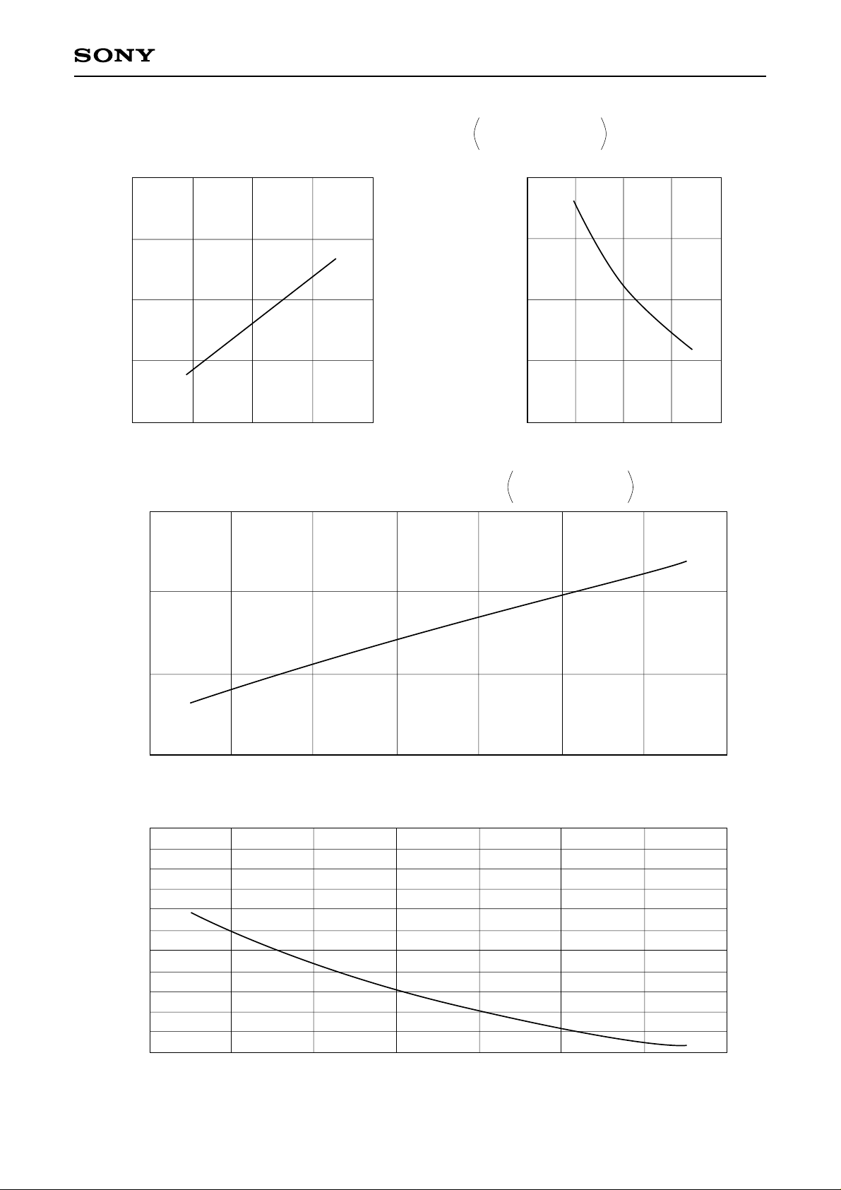
Pre-Filter Adjust characteristics
<Group Delay> <Cut Off> (fc: –3dB)
300
250
200
(nsec)
D
τ
150
100
10k 15k 20k 25k 30k
REXT [LPF ADJ1 (59PIN) ] (Ω)
Chroma Adjust characteristics
800
<Group Delay>
S1, S2 →
fc (MHz)
DL Y0 out
DL C0 out
3.0
2.5
2.0
1.5
1.0
10k 15k 20k 25k 30k
REXT [LPF ADJ1 (59PIN) ] (Ω)
S1, S2 →
R–Y out
B–Y out
600
(nsec)
D
τ
400
200
1.5
1.0
fc (MHz)
20k10k 30k 40k 50k 60k 70k 80k
EXT [LPF ADJ2 (60PIN) ] (Ω)
R
<Cut Off> (fc: –3dB)
0.5
10k 20k 30k 40k 50k 60k 70k 80k
EXT [LPF ADJ2 (60PIN) ] (Ω)
R
– 28 –
Page 29
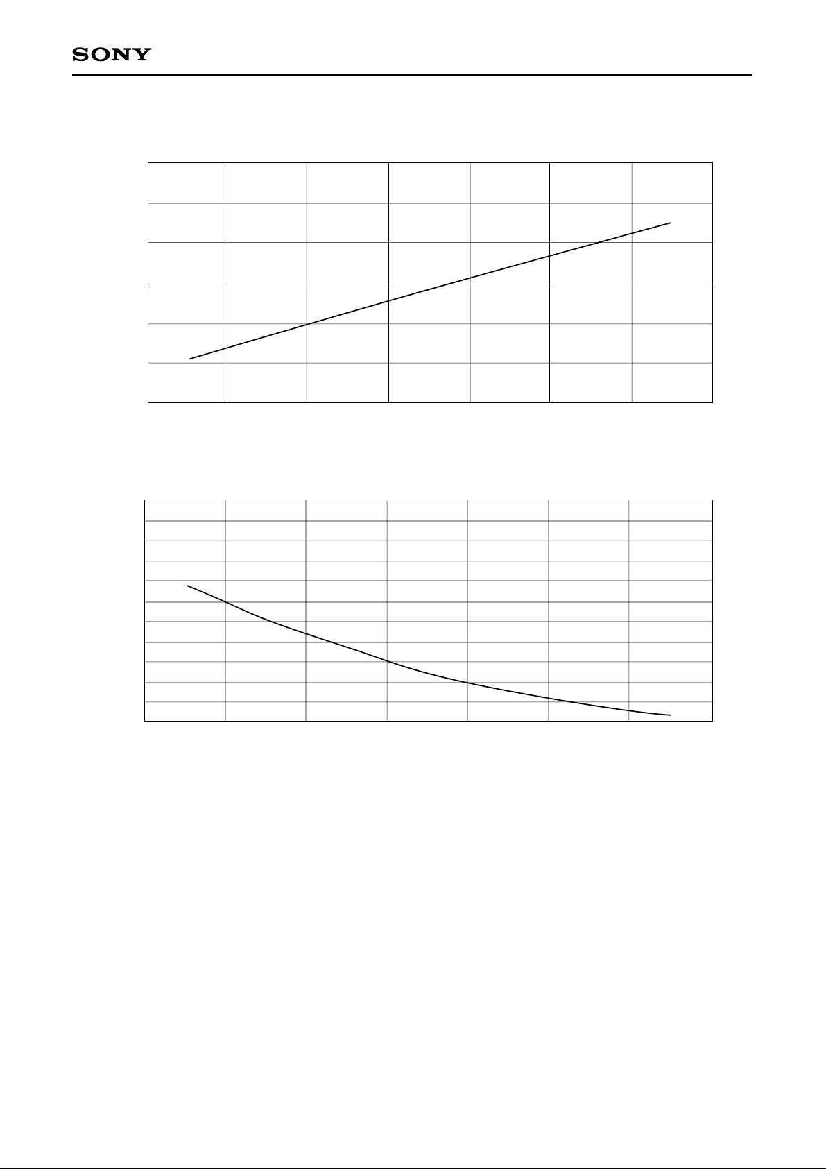
CS-VAP Adjust characteristics (S1, S2 → CS OUT)
<Group Delay>
800
600
(nsec)
D
τ
400
10k 20k 30k 40k 50k 60k 70k 80k
EXT [LPF ADJ2 (60 PIN) ] (Ω)
R
CXA1391Q/R
<Cut Off> (fc: –3dB)
1.5
1.0
fc (MHz)
0.5
10k 20k 40k 50k 60k 70k
R
EXT [LPF ADJ2 (60 PIN) ] (Ω)
80k30k
– 29 –
Page 30

CXA1391Q/R
CS-Y LPF Adjust characteristics (CS IN
→ CS OUT)
<Group Delay>
600
400
(nsec)
D
τ
200
10k 20k 30k 40k 50k 60k 70k 80k
REXT [LPF ADJ2 (60 PIN) ] (Ω)
<Cut Off> (fc: –3dB)
2.0
1.5
fc (MHz)
1.0
0.5
10k 20k 40k 50k 60k 70k 80k30k
R
EXT [LPF ADJ2 (60 PIN) ] (Ω)
VAP LPF Adjust characteristics
– 30 –
Page 31
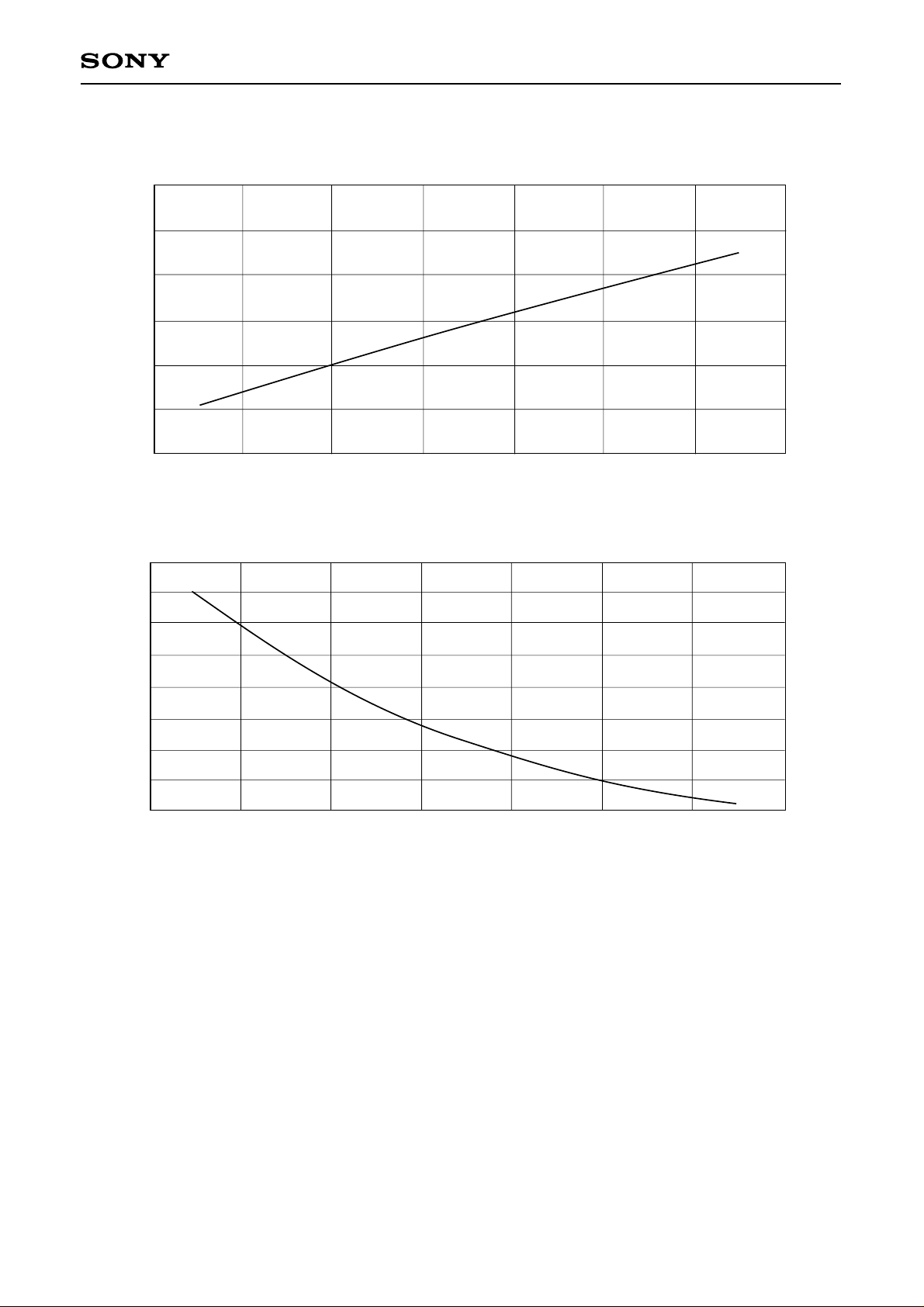
VAP LPF Adjust characteristics (S1, S2 → VAP OUT)
<Group Delay>
600
400
(nsec)
D
τ
200
10k 20k 30k 40k 50k 60k 70k 80k
REXT [LPF ADJ3 (61 PIN) ] (Ω)
CXA1391Q/R
1.5
1.0
fc (MHz)
0.5
10k 20k 40k 50k 60k 70k 80k30k
<Cut Off> (fc: –3dB)
R
EXT [LPF ADJ3 (61 PIN) ] (Ω)
– 31 –
Page 32
CXA1391Q/R
Y
Vid
C
BPF
5V
24
23
WC
CLP
SYNC
25
SETUP-
2627
SETUP
FADER-SIG
28
29
Y-LEVEL
30
SHP-OUT
31
SHP-CLP2
32
DLD
33
SHP-CLP1
DL
34
DLE
35
LEVEL
SHP-
36
YTBLK
NOISE-SLICE
38
37
19
21
22
20
18
C-IN
DGND
V-OUT
SYNC-LEVEL
VIDEO-OUT
CHROMA-OUT
FADER-MODE
CXA1392 Q/R
YH-CLP
YH-IN
YL-YH CLP
YL-YH IN
AGND
43
41
42
39
40
W/B
CONTRO LLER
IHDLIHDLIHDL
31
29
30
32
CLEVEL
WB-B
WB-G
C
SLICE
WB-DC
33
R-CLP
34
G-CLP
35
B-CLP
36
R-GAIN
37
R-CONT
38
B-CONT
39
B-GAIN
40
ID
41
B-MTX
42
MPX1-CLP
43
MPX2-CLP
44
R-MIX
45
DLCO-OUT
46
C1-GAIN
47
DLC1-IN
48
S2-IN
49
S1-IN
50
CLP
YO-
51
DLY0-
OUT
DLY1-OUT
Y1-GAIN
DLY1-IN
52
53
545556
25
27
28
26
GND
WB-R
YL-OUT
CGAM-CONT
CXA1391 Q/R
DLY2-IN
Y2-GAIN
GND
LPF-ADJ1
57
585960
14
13
16
15
17
CC
CS-Y
AV
C-OUT
MODE
CTBLK
121
CS-AGC
CBLK
11
BF
10
BFG
9
FSC-OUT
8
NC
NC
LALT
4FSC
CC
DV
R-Y CLP
R-Y IN
CLP4
CLP2
B-LEVEL
B-Y IN
B-Y
CLP
47
46
45
44
24
CS-OUT
48
21
22
23
20
R-Y
OUT
R-Y HUE
VCS-GAIN
B-Y OUT
B-Y HUE
B-Y GAIN
R-Y GAIN
CS-IN
CS-CLP
VAP-SLICE
VAP-CLP
VAP-GAIN
VAP-OUT
CLP2
CLP4
DLYH-GAIN
TP
YH-OUT2
YH-OUT1
DLYH-OUT
DLYH-CLP
DLYH-IN
CLP
YH-
LPF-ADJ2
LPF-ADJ3
VCCYGAM-
CONT
61
YH-IN
63
64
62
5V
7
6
5
4
3
5V
2
19
18
17
16
14 15
13
12
11
10
9
8
7
6
5
4
3
2
1
LPF
OUT
CT-GC
COMP-
24
YT-GC
COMP-IN
2
3
CONT
HYS-
4
CR-IN
5
CG-IN
6
CB-IN
7
GND
8
DR-IN
9
DB-IN
10
11
CLP4
12 1
23
TH-CONT
YB-IN
22
YR-IN
21
YG-IN
20
CC
V
19
DY-IN
18
DY-CLP
17
CXA1393AN/AM
YT-BLK
16
DY-OUT
CT-BLK
DB-OUT
14 15
DR-OUT
13
LPF
DL
CB
CG
CR
YB
YG
FOR TITLER
CONTRO LLER
YR
LPF IHDL
CCD
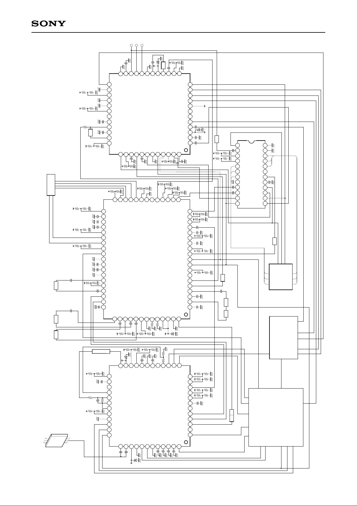
CXA Series System Diagram
5V
DETECTOR
5V
24
21
22
23
CC2
OUT
DET-
V
LEVEL
25
DET-
IRIS-GC
AGC-CLP
2627
28
29
30
31
32
33
34
35
CLP4
36
IRIS-LEVEL
AGC-OUT
OPIN-P
OPIN-N
OP-OUT
AGC-CONT
AGC-MAX
AGC-SEL
XSHP
XSHD
CC1
XSP3
PG-IN
DATA-IN
V
38
37
39
40
20
DET-CLP
XSP2
41
19
GND
XSP1
42
17
18
IRIS-CLP
CXA1390 Q/R
GND
43
14
13
16
15
WND
VG-OUT
IRIS-OUT
FSHI
F3-CLP
F2-CLP
45
44
SL
CLP1
PBLK
CS-AGC-
121
CS-A GC-GC
11
CS-OUT
10
CS-CCD-GC
9
CS-CCD-SL
8
CS-CLP
7
F3-OUT
6
F2-OUT
5
F1-OUT
4
GY-OUT
3
DC-OUT
2
XSH1
F1-CLP
XSH2
46
48
47
DL
LPF
CLP2
XSH2 CLP1 ID PBLK
XSH1
XSP1
XSP2
SG
BF SYNC LALT 4fSC
WND
BLK
HD.VD CL
BFG
TG
CLP4
XSHD
XSHP
5V
– 32 –
Page 33

Package Outline Unit: mm
CXA1391Q
CXA1391Q/R
64PIN QFP(PLASTIC)
52
64
SONY CODE
EIAJ CODE
JEDEC CODE
23.9 ± 0.4
+ 0.4
20.0 – 0.1
51
1
1.0
+ 0.15
0.4 – 0.1
33
32
+ 0.4
14.0 – 0.1
17.9 ± 0.4
20
19
± 0.12
+ 0.35
2.75 – 0.15
M
0.15 – 0.05
+ 0.2
0.1 – 0.05
+ 0.1
0.15
16.3
0.8 ± 0.2
PACKAGE STRUCTURE
QFP–64P–L01
∗
QFP064–P–1420
PACKAGE MATERIAL
LEAD TREATMENT
LEAD MATERIAL
PACKAGE WEIGHT
EPOXY RESIN
SOLDER/PALLADIUM
PLATING
COPPER /42 ALLOY
1.5g
CXA1391R
49
64
0.5 ± 0.08
SONY CODE
EIAJ CODE
JEDEC CODE
∗ 10.0 ± 0.1
48
1
0.1 ± 0.1
0° to 10°
64PIN LQFP (PLASTIC)
12.0 ± 0.2
33
16
+ 0.08
0.18 – 0.03
0.5 ± 0.2
DETAIL A
LQFP-64P-L01
∗QFP064-P-1010-A
32
(11.0)
+ 0.2
1.5 – 0.1
A
0.5 ± 0.2
+ 0.05
0.127 – 0.02
0.1
17
(0.22)
NOTE: Dimension “∗” does not include mold protrusion.
PACKAGE STRUCTURE
PACKAGE MATERIAL
LEAD TREATMENT
LEAD MATERIAL
PACKAGE WEIGHT
EPOXY / PHENOL RESIN
SOLDER PLATING
42 ALLOY
0.3g
– 33 –
 Loading...