

Page 1
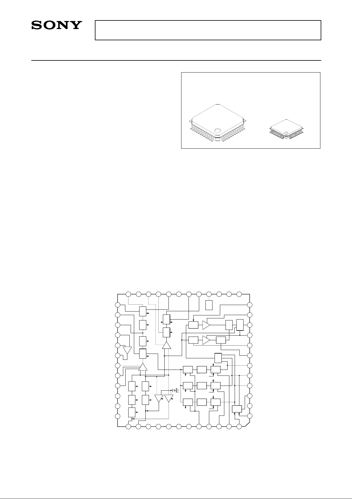
CXA1390AQ/AR
S/H and AGC for CCD Camera
Description
The CXA1390AQ/AR are CCD camera's signal
processing ICs which extract signals from the CCD
output. These bipolar ICs perform correlated double
sampling. AGC, color separation, high luminance
detection and others. Additionary, these ICs are not
affected by irregular pulses which occure during the
CCD shutter mode.
Featuers
• Pin compatible upgraded version of CXA1390Q/R
which can be swapped out while using same
peripheral chips
• Almost completely corrects irregular pulses and
their negative affects
• Correlated double sampling function alllows for the
suppression of low band noise in the CCD output
• AGC amplifier, which has High S/N ratio and wide
gain control range, enhances the camera sensitivity
• Output for iris adjustment. High luminance
detection output
• Usage of Vg (regulator) output allows for the
formation of IRIS and AGC LOOP which are not
affected by supply voltage functation
Operating Conditions
Supply voltage VCC 4.75 to 5.25 V
CXA1390AQ
48 pin QFP (Plastic)
CXA1390AR
48 pin LQFP (Plastic)
Application
S/H and AGC for CCD camera
Structure
Bipolar silicon monolithic IC
Absolute Maximum Ratings (Ta = 25°C)
• Supply voltage VCC 12 V
• Operating temperature Topr –20 to +75 °C
• Storage temperature Tstg –65 to +150 °C
• Allowable power dissipation
PD 600 (QFP) mW
950 (VQFP) ∗mW
∗
(40mm × 40mm, t = 0.8mm with a mounted glass epoxy
substrate)
Block Diagram and Pin Configuration (Top View)
CC2
DET OUT
V
IRIS GC
IRIS LEVEL
21
22
CLP
CLP1
CLP1
WND
WND
BLK
PBLK
CLP
CLP1
AGC
SH
XSHP
SH
XSHD
COM
40
39
1
CC
V
XSP3
DET LEVEL
AGC CLP
AGC OUT
OP IN +
OP IN –
OP OUT
AGC CONT
AGC MAX
AGC SEL
XSHP
XSHD
CLP4
23
24
25
26
27
28
29
OP
30
31
32
33
SH
XSHP
34
SHSH
35
36
XSHD
XSHP
37
38
PG IN
DATA IN
DET CLP
GND
IRIS CL P
IRIS OUT
VG OUT
WND
PBLK
CLP1
19
18
17
20
BLK
CLP
WND
GC
CLP4
41
XSP2
COM
SLICE
WND PBLK
SLICE
SH
XSP3
SH
XSP2
CLP4
SH
XSP1
43
42
XSP1
16
VG
GC
CLP
GC
MAX
CLP1
CLP
LPF
BLK
PBLK
CLP1
CLP
LPF
BLK
PBLK
CLP1
CLP
LPF
BLK
PBLK
46
45
44
GND
FSH1
F3 CLP
13
1415
12
CSAGC SL
CSAGC GC
11
CS OUT
F1 CLP
GATE
10
SW
MODE
9
CS CCD GC
CS CCD SL
8
CS CLP
7
F3 OUT
6
5
F2 OUT
4
F1 OUT
GY OUT
3
DC OUT
2
1
XSH1
48
XSH2
OR
47
F2 CLP
Sony reserves the right to change products and specifications without prior notice. This information does not convey any license by
any implication or otherwise under any patents or other right. Application circuits shown, if any, are typical examples illustrating the
operation of the devices. Sony cannot assume responsibility for any problems arising out of the use of these circuits.
– 1 –
E90941A78
Page 2
CXA1390AQ/AR
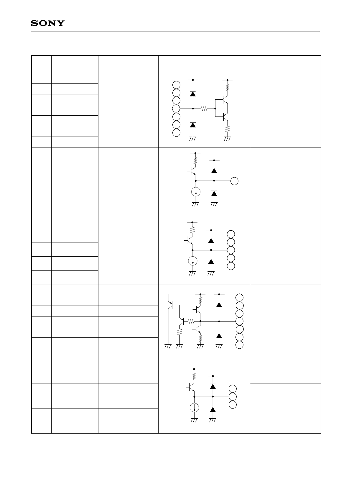
Pin Description and Standard Pin voltage (VCC = 5V)
PIn
No.
1
34
35
40
41
42
48
2
3
4
5
6
Symbol
XSH1
XSHP
XSHD
XSP3
XSP2
XSP1
XSH2
DC OUT
GY OUT
F1 OUT
F2 OUT
F3 OUT
Voltage
H: 4V and above
L: 1V and below
1.8 to 2.1V
Black level
1.8 to 2.1V
Equivalent circuit
1
34
35
40
41
42
48
180µA
360µA
130
1k
300
3
4
6
27
5
200
200
2
Description
High speed pulse input
pin for S/H (active at L)
DC output pin of f1 to f3
output black level
Signal output pin
27
7
18
20
26
45
46
47
10
17
24
AGC OUT
CS CLP
IRIS CLP
DET CLP
AGC CLP
F3 CLP
F2 CLP
F1 CLP
CS OUT
IRIS OUT
DET OUT
2.6 to 3.3V
2.0 to 2.6V
1.9 to 2.6V
2.3 to 2.8V
2.0 to 2.6V
2.0 to 2.6V
2.0 to 2.6V
1.7 to 2.2V
1.7 to 2.0V
1.7 to 2.0V
200µA
130
300
10
17
24
7
18
20
Capacitor connecting
26
45
46
47
pin for clamp
Signal output pin
Signal output pin Vcc
fluctuations effect is
minor on DC level
– 2 –
Page 3
CXA1390AQ/AR
PIn
No.
8
9
11
12
21
22
25
31
32
Symbol
CS CCD SL
CS CCD GC
CSAGC GC
CSAGC SL
IRIS LEVEL
IRIS GC
DET LEVEL
AGC CONT
AGC MAX
Voltage
(Test mode at 0V)
Equivalent circuit
8
9
11
12
21
22
25
31
32
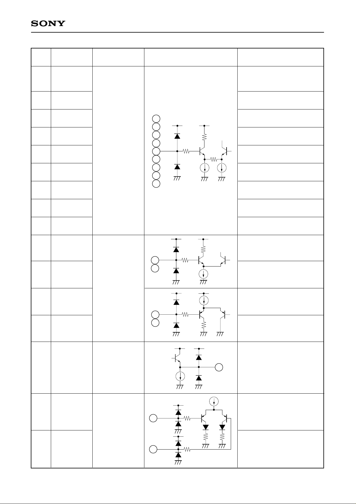
Description
Level adjustment pin of high
luminance detection pin of the
input signal
Gain adjustment pin of input
signal high luminance part
Gain adjustment pin of high
luminance port after AGC
Level adjustment pin of high
luminance detection after AGC
130
Adjustment pin of IRIS output
weighting (Active at WND = L)
Gain adjustment pin of IRIS
output
Adjustment pin of DET output
weighting (Active at WND = L)
AGC amplifier gain
adjustment pin
AGC amplifier MAX gain
adjustment pin
13
14
15
36
16
28
CLP1
P BLK
WND
CLP4
VG OUT
OP IN +
H: 4V and above
L: 1V and below
2.6 to 3.1V
28
13
14
15
36
100µA
130
130
130
16
CLP1 pulse input pin
Active at H (OPB clamp)
Pre BLK pulse input pin
Active at L
Window pulse input pin
Active at L
CLP4 pulse input pin
Active at H
Regulator output pin
(Used for the formation of
AGC and IRIS loop)
Operation amplifier non
inverted input pin
29
OP IN –
1 to 3.3V
29
– 3 –
130
Operation amplifier inverted
input pin
Page 4
CXA1390AQ/AR
PIn
No.
30
33
Symbol
OP OUT
AGC SEL
Voltage
H: 4.2V and above
L: 1.2V and below
VCC: Low Gain mode
GND: High Gain mode
Equivalent circuit
3.3V
500µA
50k
3.6V
33
100µA
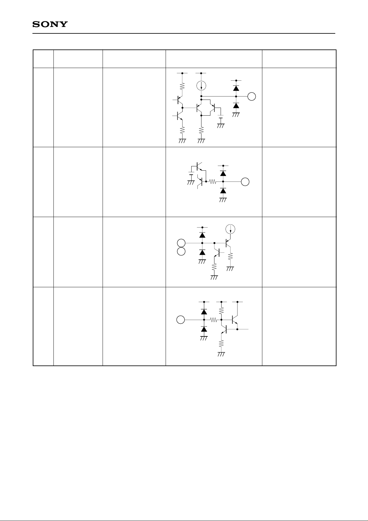
Description
30
Output pin
AGC amplifier gain
selection pin
37
38
44
PG IN
DATA IN
FSHI
Black level
2.7 to 3.2V
1.4 to 1.8V
44
37
38
130
8.5k
CCD signal input pin
Adjustment pin for color
separation S/H follow up
speed
(Normally used OPEN)
– 4 –
Page 5
CXA1390AQ/AR
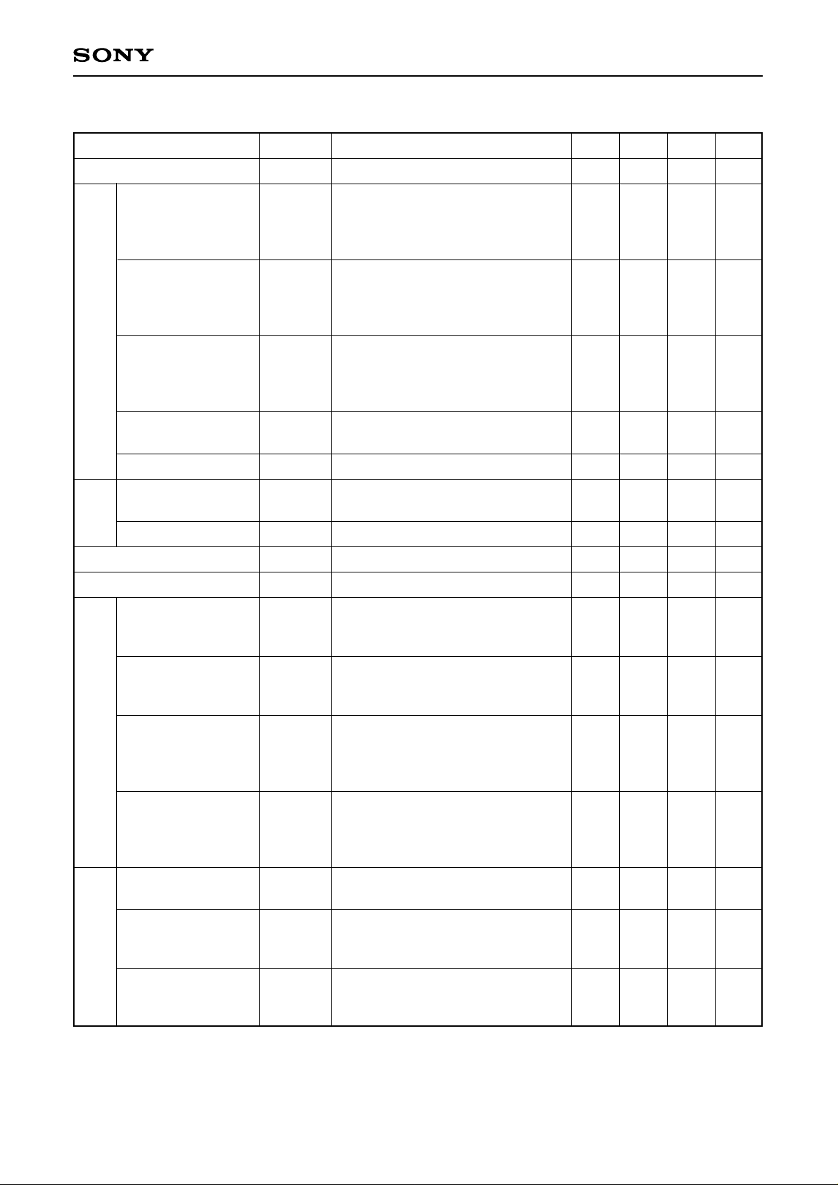
Electrical Characteristics
Current consumption
CONT Min.
CONT Max.
AGC
Max. Min.
Gain shift
BLK offset
Color
Gain
separation
BLK offset
(Ta = 25°C, VCC = 5.0V)
SymbolItem Conditions Min. Typ. Max. Unit
ID
32 48 65 mA
AGC OUT/DATA IN
ACON
Min.
AGC CONT = 1.5V
AGC MAX = 5V
68dB
AGC SEL = 0V
AGC OUT/DATA IN
ACON
Max.
AGC CONT = 4.5V
AGC MAX = 5V
30 32 dB
AGC SEL = 0V
AGC OUT/DATA IN
MAX
Min.
AGC CONT = 4.5V
AGC MAX = 1.5V
17 20 dB
AGC SEL = 0V
GSHI
∆BLK
f Gain
f ∆BLK
AGC OUT (SEL = 5V) /AGC OUT
(SEL = 0V)
Note 1)
Color separation output/AGC OUT
(f1, f2, f3)
Note 1)
–5 –4 –3 dB
–10 0 +10 mV
–0.5 0 +0.5 dB
–10 0 +10 mV
DC OUT
Gate Gain
Gain Cont Max.
Gain Cont Min.
IRIS
Window Level Max.
Window Level Min.
Gain
DET
Window Level Max.
DC
GY
IR Max.
IR Min.
IRW
Max.
IRW
Min.
DET G
DET
Max.
GY OUT/AGC OUT
IRIS OUT/DATA IN
IRIS GC = 5V
WND = 5V
IRIS OUT/DATA IN
IRIS GC = 1.5V
WND = 5V
Gain Cont Max. ratio (attenuation)
IRIS GC = 1.5V
IRIS LEVEL = 5V
WND = 0V
Gain Cont Max. ratio (attenuation)
IRIS GC = 1.5V
IRIS LEVEL = 1.5V
WND = 0V
DET OUT/AGC OUT
WND = 5V
DET OUT/AGC OUT
DET LEVEL = 5V
WND = 0V
1.8 1.95 2.1 V
–0.5 0 +0.5 dB
18 22
4
–1
0
8
–14
dB
dB
dB
dB
–2 –1 +0.5 dB
–2
–1
+0.5 dB
Window Level Min.
DET
Min.
Level Max. ratio
DET LEVEL = 1.5V
WND = 0V
– 5 –
–13 dB
Page 6
CS
CCD
Max. Gain
Min. Gain
CXA1390AQ/AR
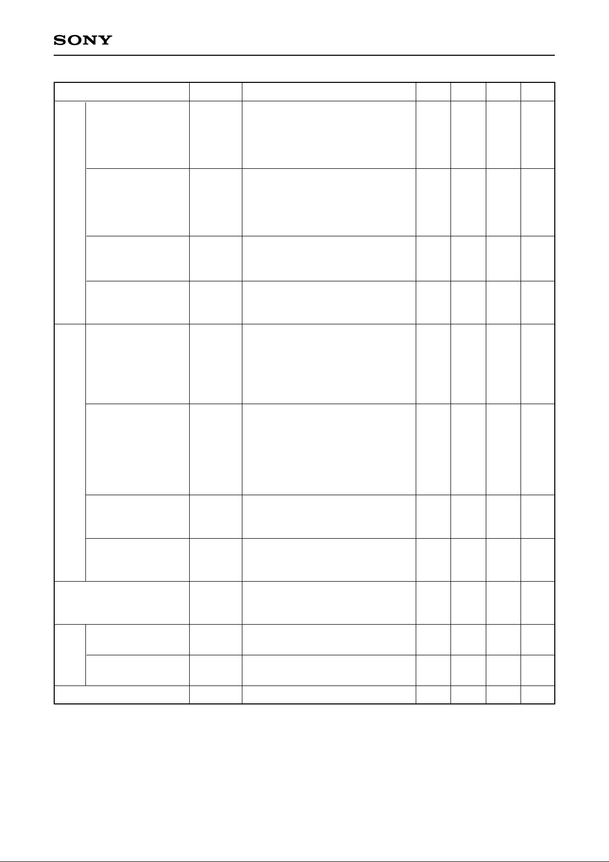
SymbolItem Conditions Min. Typ. Max. Unit
CSOUT differential/
CSC
Max.
DATA IN differential
CS CCD SL = 4.1V
CS CCD GC = 5V
13
16
dB
PBLK = 0V
CSOUT differential/
CSC
Min.
DATA IN differential
CS CCD SL = 4.1V
CS CCD GC = 1.5V
–1 1 dB
PBLK = 0V
CS
AGC
Max. SLICE
Min. SLICE
Max. Gain
Min. Gain
Max. SLICE
CSC
Max. SL
CSC
Min. SL
CSA
Max.
CSA
Min.
CSA
Max. SL
Input conversion slice level
CS CCD SL = 1.5V
Note 1)
Input conversion slice level
CS CCD SL = 5V
Note 1)
CS OUT DATA IN = 0.2Vpp
CS AGC GC = 5V
CS AGC SL = 4.2V
CS CCD GC = 1.5V
CS CCD SL = 1.5V
Note 2)
CS OUT differential/
AGC OUTdifferential
CS AGC GC = 1.5V
CS AGC SL = 4.2V
CS CCD GC = 1.5V
CS CCD SL = 1.5V
Note 2)
AGC OUT conversion
CS AGC SL = 1.5V
Note 3)
0.7
0.5
1.2
V
40 100 mV
Vpp
–1 1 dB
V
Min. SLICE
CSA
Min. SL
TEST mode TEST
H level
OPH
OPAmp
L level
Vg OUT
OPL
Vg At no load 2.6 2.85 3.1
AGC OUT conversion
CS AGC SL = 5V
Note 3)
DATA IN = 0.5Vpp
CS CCD GC = 0V
Note 4)
OP IN + = 2.1V
OP IN – = 2.0V
OP IN + = 2.0V
OP IN – = 2.1V
– 6 –
0.06 0.1 V
0.5 Vpp
4.2 V
0.9 1.2 V
V
Page 7
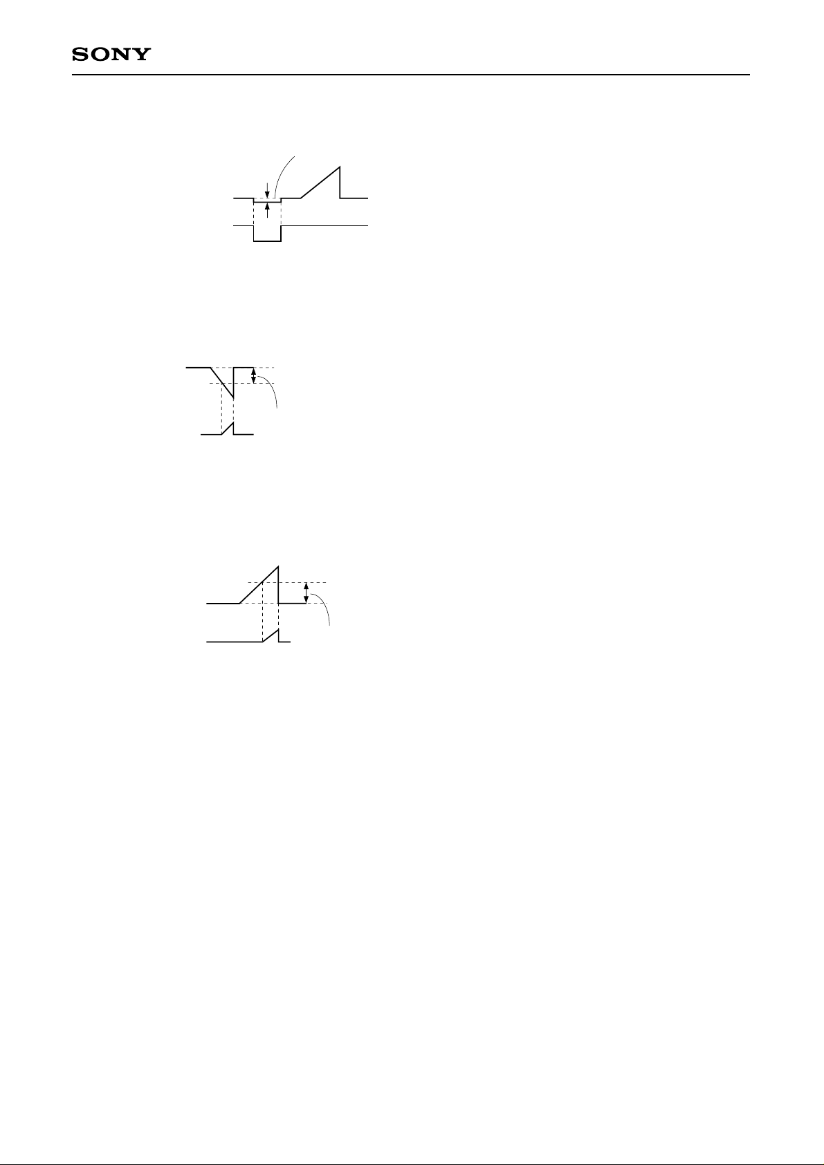
Note 1)
CXA1390AQ/AR
Indicates the specification
Output signal
BLK input
5
0
Note 2)
Voltage between DATA IN input black level and the high luminance level determined by CS CCD SL pin voltage.
Black level
DATA IN
CS OUT
High luminance level
Indicates the specification
Note 3)
Voltage between the black level at AGC OUT and the high luminance level determined by CS AGC SL pin voltage.
High luminance level
AGC OUT
Black level
CS OUT
Indicates the specification
Note 4)
S/H output DATA IN input can be monitored by turning CS CCD GC (Pin 9) to 0V.
– 7 –
Page 8
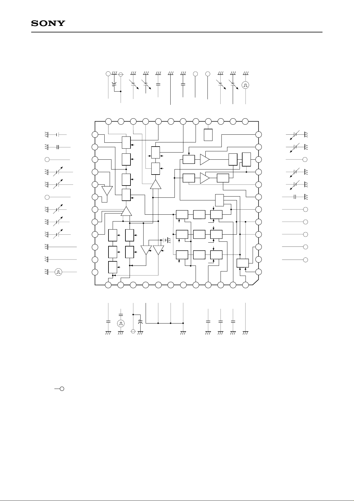
Test Circuit
(3V) (3V) (3V) (3V)
V
CC 5V
CXA1390AQ/AR
(3V)
(2V)
(2V)
(1.5V)
(5V)
(0V)
0.1
CLP4
DET LEVEL
AGC CLP
AGC OUT
OP IN +
OP IN –
OP OUT
AGC CONT
AGC MAX
AGC SEL
XSHP
XSHD
CLP4
0.1 0.1
CLP2
10µ
2
24
DET OUT
CC
V
23
IRIS LEVEL
IRIS G C
21
22
GND
DET CLP
19
20
IRIS O UT
IRIS C L P
18
17
25
SH
SHSH
CLP
CLP1
CLP1
BLK
CLP
WND
WND
WND
WND PBLK
BLK
PBLK
CLP
CLP1
AGC
SH
XSHP
SH
XSHD
XSHP
GC
SH
XSP3
COM
SH
XSP2
CLP4
SH
XSP1
XSHP
XSHD
CLP4
COM
SLICE
SLICE
GC
GC
LPF
PBLK
LPF
PBLK
LPF
PBLK
26
27
28
29
OP
30
31
32
33
34
35
36
VG OUT
16
VG
CLP1
CLP1
CLP1
CLP
BLK
CLP
BLK
CLP
BLK
WND
CLP
MAX
CLP1
PBLK
13
1415
12
OR
CSAGC SL
CSAGC GC
11
CS OUT
10
SW
MODE
9
CS CCD GC
CS CCD SL
8
CS CLP
7
(3V )
(3V)
(3V)
(3V)
0.1
F3 OUT
6
5
F2 OUT
4
F1 OUT
GY OUT
3
DC OUT
GATE
2
1
XSH1
37
38
PG IN
DAT A IN
40
39
1
CC
V
XSP3
41
XSP2
42
XSP1
43
44
GND
FSH1
46
45
F2 CLP
F3 CLP
48
47
XSH2
F1 CLP
0.1
0.1
0.1
10µ
IN
V
CC 5V
0.1 0.1
Note 1) Capacitor unit value at µF.
Note 2) Voltage in parentheses are those not specified in the Electrical Characteristics Test Conditions.
Note 3) indicates a test pin. (For both AC and DC)
– 8 –
Page 9
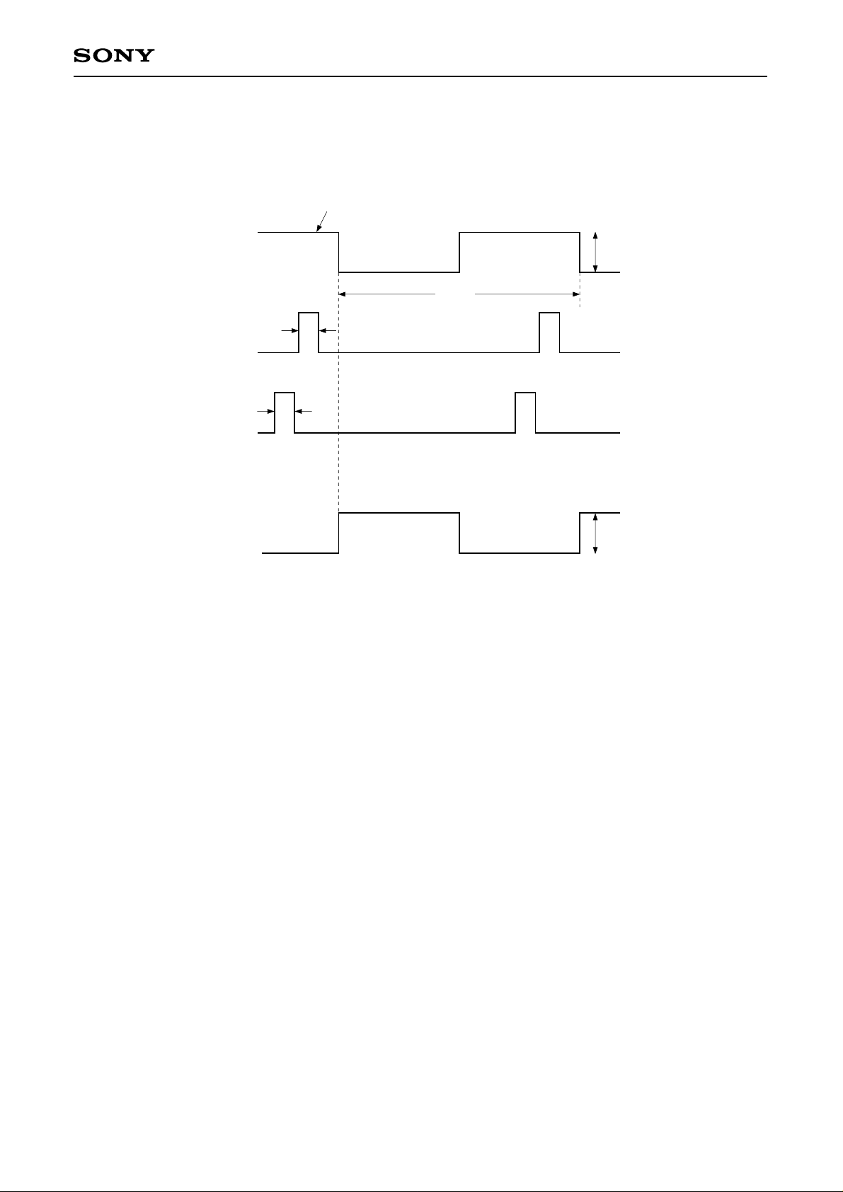
Timing Diagram for Testing
DATA IN input
CXA1390AQ/AR
Equivalent to black
Differs with every test
CLP 1
CLP 4
Output waveform
AGC OUT
IRIS OUT
F1 to F3 OUT
GY OUT
DET OUT
CS OUT
5V
5V
2µsec
0
2µsec
0
1H
Output signal level
– 9 –
Page 10

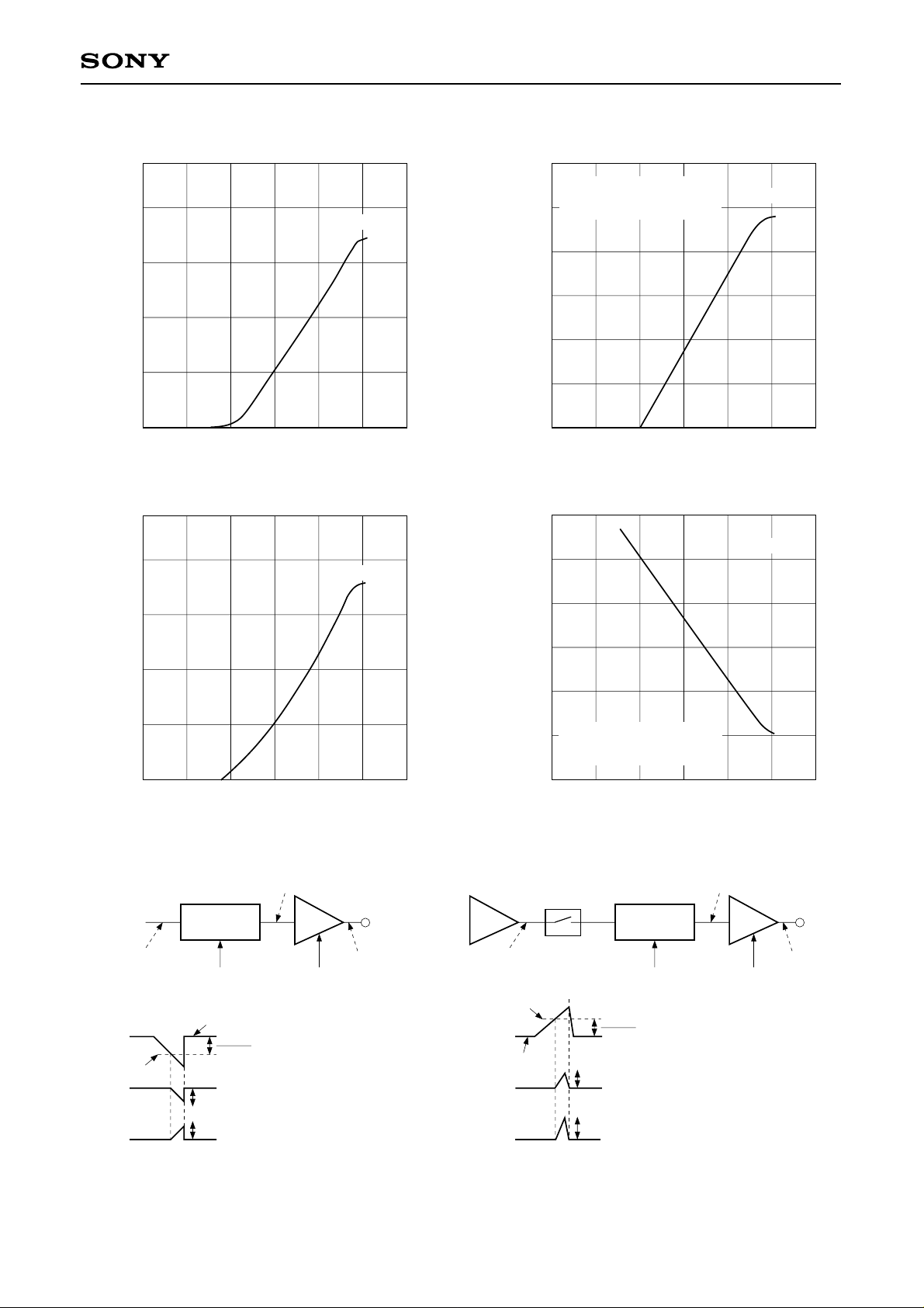
Standard Control Characteristics (VCC = 5V, Ta = 25°C)
CXA1390AQ/AR
AGC amplifier gain control characteristics
dB
30
25
20
15
10
5
012345V
AGC CONT voltage
(AGC Max. = 5V)
IRIS gain control characteristics
dB
25
20
15
10
5
0
012345V
IRIS GC voltage
AGC maximum control characteristics
dB
30
20
10
5
012345V
AGC maximum voltage
(AGC CONT = 5V)
IRIS WINDOW control characteristics
(Weighting characteristics)
dB
(WND = 0V)
Gain control characteristics
when IRIS LEVEL=5V is set at 0dB
0
–5
–10
–15
–20
12345V
IRIS LEVEL voltage
DET WINDOW control characteristics
(Weighting characteristics)
dB
(WND = 0V)
Gain control characteristics
when DET LEVEL = 5V is set at 0dB
0
–5
–10
–15
–20
12345V
DET LEVEL voltage
– 10 –
Page 11
CXA1390AQ/AR
CS CCD gain control characteristics
dB
20
15
10
5
0
012345V
CS CCD GC voltage
Note 1-a
CS AGC gain control characteristics
dB
20
Note 2-a
CS CCD slice control characteristics
V
(High luminance detection
level control)
0
Input conversion value
0.2
0.4
0.6
0.8
1.0
012 345V
CS CCD SL voltage
Note 1-b
CS AGC slice control characteristics
V
1.6
Note 2-b
15
10
5
0
Note 1-a, 1-b
(1)
(1)
Detection level
(2)
(3)
12345V
CS AGC GC voltage
(2)
CS OUTDATA IN
SLICE
CS CCD SL CS CCD GC
Black level
GCA
(3)
Note 1-b
Voltage indicated at CS CCD
slice control characteristics
Note 1-a
Characteristics indicated at CS CCD
gain control characteristics
=ratio of 3 and 2 (dB)
Note 2-a, 2-b
SEPARATION
AGC
(1)
Detection level
(1)
Black level
(2)
(3)
1.2
0.8
0.4
(High luminance detection
0
level control after AGC)
Input conversion value
12345V
COLOR
CS AGC SL CS AGC GC
CS AGC SL voltage
(2)
CS OUT
SLICE
Note 2-b
Voltage indicated at CS AGC
slice control characteristics
Note 2-a
Characteristics indicated at CS AGC
slice control characteristics
=ratio of 3 and 2 (dB)
GCA
(3)
– 11 –
Page 12
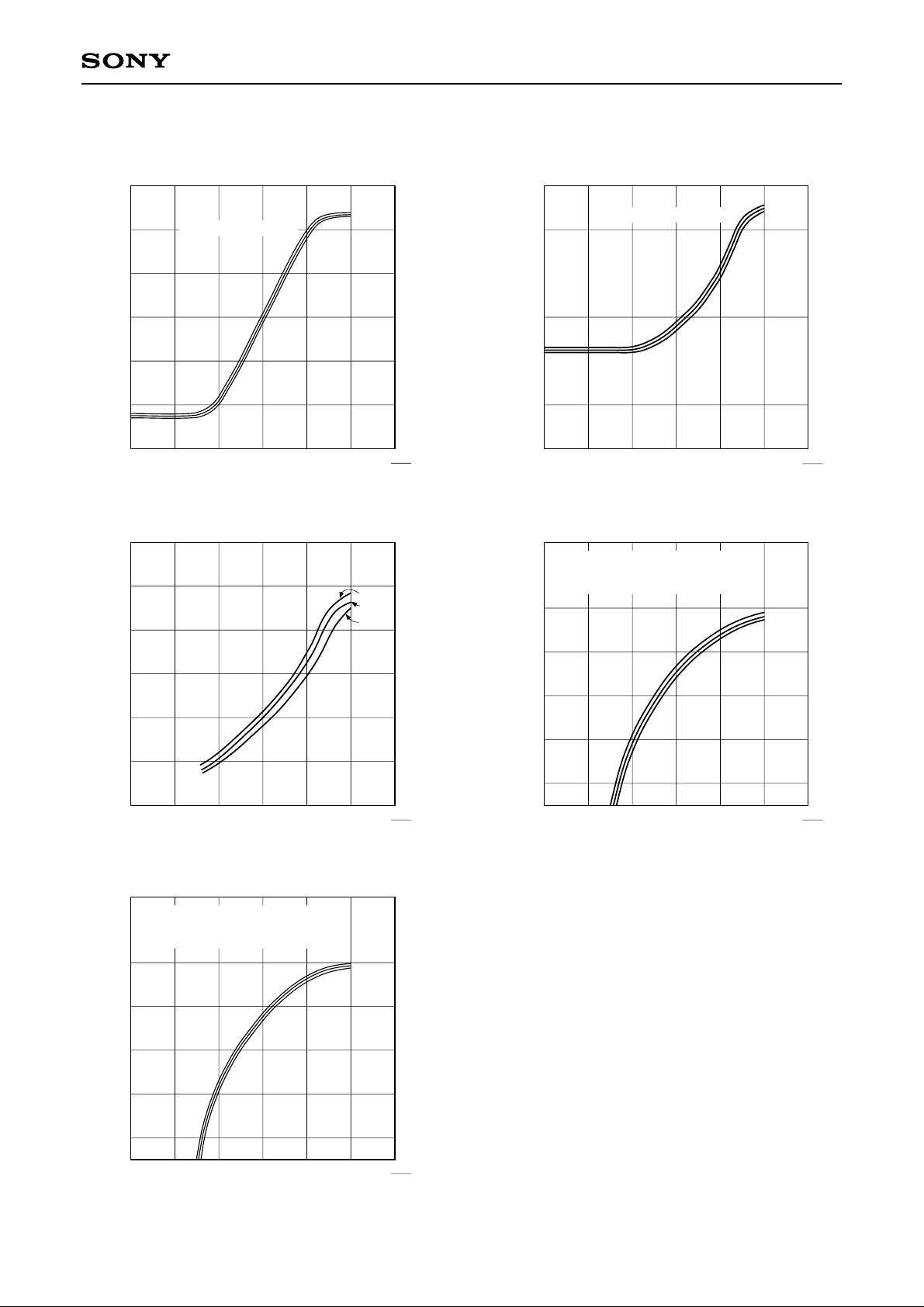
Supply voltage Characteristics Standard Design Documentation (Ta = 25°C)
CXA1390AQ/AR
AGC amplifier gain control characteristics
dB
30
25
20
15
10
5
012345
(AGC Max. = VCC)
AGC CONT voltage
IRIS gain control characteristics
dB
25
20
15
10
5
0
012345
IRIS GC volage
5V5.25V
4.75V
(× )
5.25V
5V
4.75V
×
VCC
5
VCC
5
AGC maximum control characteristics
dB
(AGC CONT = VCC)
30
20
10
5
012345
AGC maximum voltage
5.25V
4.75V
IRIS WINDOW control characeristics
(Weighting characteristics)
dB
WND = 0V
Gain control characteristics when
IRIS LEVEL = Vcc is set at 0dB
0
–5
–10
–15
–20
12345
IRIS LEVEL voltage
4.75V
5V
VCC
(× )
5
5V5.25V
VCC
(× )
5
DET WINDOW control
(Weighting characteristics)
dB
WND=0V
Gain control characteristics when
DET LEVEL=Vcc is set at 0dB
0
–5
–10
–15
–20
12345
DET LEVEL voltage
5.25V
4.75V
5V
VCC
(× )
5
– 12 –
Page 13
CXA1390AQ/AR
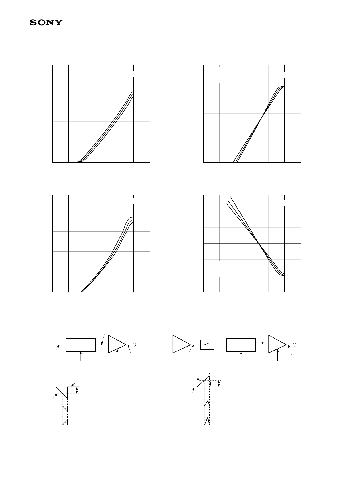
CS CCD gain control characteristics
dB
Note 1-a
20
15
10
5
0
012345
CS CCD GC voltage
5.25V
CS AGC gain control characteristics
dB
Note 2-a
20
15
5.25V
5V
4.75V
(× )
5V
4.75V
CS CCD slice control characteristics
V
(High luminance detection
level control)
Input conversion value
0
0.2
0.4
0.6
0.8
CC
V
5
1.0
012345
CS CCD SL voltage
5.25V
4.75V
Note 1-b
5V
V
CC
(× )
5
CS AGC slice control characteristics
V
Note 2-b
1.6
1.2
10
5
0
Note 1-a, 1-b
(1)
(1)
Detection level
(2)
(3)
12345
CS AGC GC voltage
(2)
SLICE
CS CCD SL CS CCD GC
Black level
GCA
Note 1-b
Voltage indicated at CS CCD
slice control characteristics
Note 1-a
Characteristics indicated at CS CCD
gain control characteristics
=ratio of 3 and 2 (dB)
(× )
CS OUTDATA IN
(3)
0.8
0.4
(High luminance detection
level control after AGC)
Input conversion value
0
CC
V
5
Note 2-a, 2-b
AGC
Detection level
Black level
COLOR
SEPARATION
(1)
(1)
(2)
(3)
12345
CS AGC SL voltage
SLICE
CS AGC SL CS AGC GC
Note 2-b
Voltage indicated at CS AGC
slice control characteristics
Note 2-a
Characteristics indicated at CS AGC
slice control characteristics
=ratio of 3 and 2 (dB)
(2)
4.75V
5.25V
GCA
5V
V
CC
(× )
5
CS OUT
(3)
– 13 –
Page 14
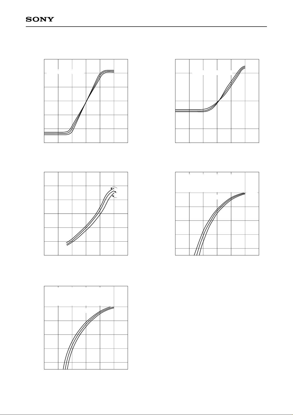
Standard Design Documentation Temperature Characteristics (VCC = 5V)
CXA1390AQ/AR
AGC amplifier gain control characteristics
dB
(AGC Max. = VCC)
30
25
20
15
10
5
012345
AGC CONT voltage
–20°C
IRIS gain control characteristics
dB
25
20
15
10
5
0
012345
IRIS GC voltage
25°C
75°C
–20°C
25°C
75°C
AGC maximum control characteristics
dB
30
20
10
5
V
012345
(AGC CONT = VCC)
AGC maximum voltage
–20°C
25°C
75°C
V
IRIS WINDOW control characteristics
(Weighting characteristics)
dB
(WND = 0V)
Gain control characteristics
when IRIS LEVEL = VCC, Ta=25°C
is set at 0dB.
0
–5
–10
–15
–20
V
12345
IRIS LEVEL voltage
–20°C
25°C
75°C
V
DET WINDOW control
(Weighting characteristics)
dB
(WND = 0V)
Gain control characteristics
when DET LEVEL = VCC, Ta = 25°C
is set at 0dB.
0
–5
–10
–15
–20
12345
–20°C
DET LEVEL voltage
25°C
75°C
V
– 14 –
Page 15
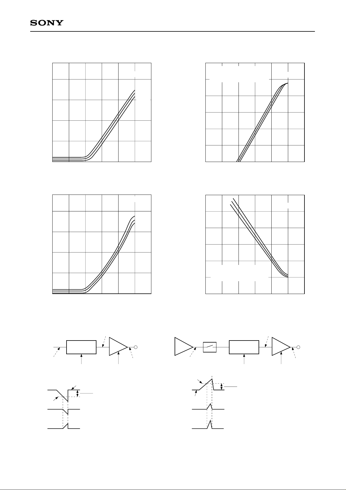
CXA1390AQ/AR
CS CCD gain control characteristics
dB
20
15
10
5
0
012345V
CS CCD GC voltage
Note 1-a
–20°C
25°C
75°C
CS AGC gain control characteristics
dB
20
15
Note 2-a
–20°C
25°C
75°C
CS CCD slice control characteristics
V
(High luminance detection
level control)
Input conversion value
0
0.2
0.4
0.6
0.8
1.0
012 345
CS CCD SL voltage
–20°C
CS AGC slice control characteristics
V
1.6
1.2
Note 1-b
25°C
75°C
V
Note 2-b
10
5
0
Note 1-a, 1-b
(1)
(1)
Detection level
(2)
(3)
12345
CS AGC GC voltage
(2)
CS OUTDATA IN
SLICE
CS CCD SL CS CCD GC
Black level
GCA
(3)
Note 1-b
Voltage indicated at CS CCD
slice control characteristics
Note 1-a
Characteristics indicated at CS
CCD gain control characteristics
=ratio of 3 and 2 (dB)
0.8
0.4
(High luminance detection
level control after AGC)
0
Input conversion value
V
Note 2-a, 2-b
COLOR
SEPARATION
AGC
(1)
Detection level
(1)
Black level
(2)
(3)
12345
CS AGC SL voltage
(2)
SLICE
CS AGC SL CS AGC GC
Note 2-b
Voltage indicated at CS AGC
slice control characteristics
Note 2-a
Characteristics indicated at CS
AGC slice control characteristics
=ratio of 3 and 2 (dB)
75°C
25°C
–20°C
V
CS OUT
GCA
(3)
– 15 –
Page 16
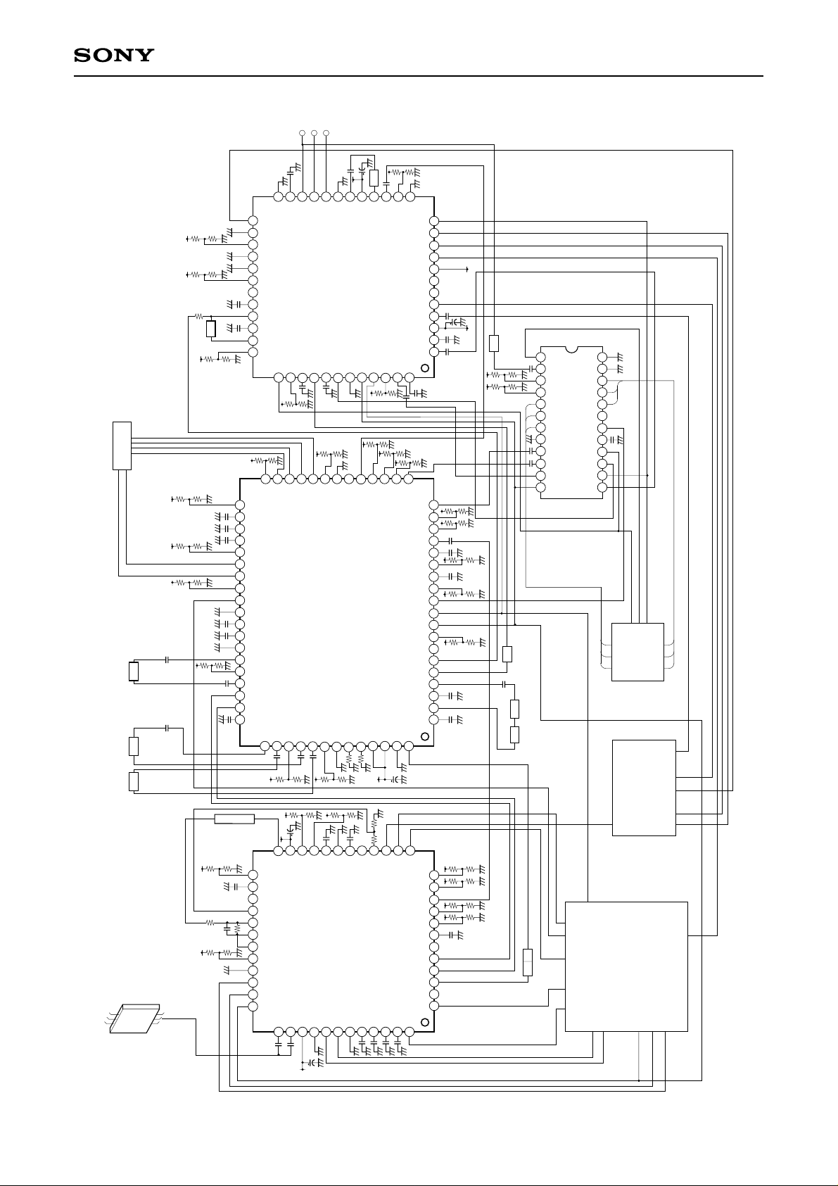
CXA1390AQ/AR
Y
Vid
C
BPF
5V
24
23
WC
CLP
SYNC
25
SETUP-
26
SETUP
27
FADER-SIG
28
29
Y-LEVEL
30
SHP-OUT
31
SHP-CLP2
32
DLD
33
SHP-CLP1
DL
34
DLE
35
LEVEL
SHP-
36
YTBLK
NOISE-SLICE
38
37
19
21
22
20
18
C-IN
DGND
V-OUT
SYNC-LEVEL
VIDEO-OUT
CHROMA-OUT
FADER-MODE
CXA1392Q/R
YH-CLP
YH-IN
YL-YH CLP
YL-YH IN
AGND
43
41
42
39
40
W/B
CONTROLLER
IHDL
IHDLIHDL
31
29
30
32
C-
LEVEL
WB-B
WB-G
C
SLICE
WB-DC
33
R-CLP
34
G-CLP
35
B-CLP
36
R-GAIN
37
R-CONT
38
B-CONT
39
B-GAIN
40
ID
4142
B-MTX
MPX1-CLP
43
MPX2-CLP
44
R-MIX
45
DLCO-OUT
46
C1-GAIN
47
DLC1-IN
48
S2-IN
49
S1-IN
50
CLP
YO-
51
DLY0-
OUT
DLY1-OUT
Y1-GAIN
DLY1-IN
52
53
545556
25
27
28
26
GND
WB-R
YL-OUT
CGAM-CONT
CXA1391 Q/R
DLY2-IN
Y2-GAIN
GND
LPF-ADJ1
57
585960
14
13
16
15
17
CC
CS-Y
AV
C-OUT
MODE
CTBLK
121
CS-AGC
CBLK
11
BF
10
BFG
9
FSC-OUT
8
NC
NC
LALT
4FSC
CC
DV
R-Y CLP
R-Y IN
CLP4
CLP2
B-LEVEL
B-Y IN
B-Y
CLP
47
46
45
44
24
CS-OUT
48
21
22
23
20
R-Y
OUT
B-Y OUT
R-Y HUE
B-Y HUE
VCS-GAIN
B-Y GAIN
R-Y GAIN
CS-IN
CS-CLP
VAP-SLICE
VAP-CLP
VAP-GAIN
VAP-OUT
CLP2
CLP4
DLYH-GAIN
TP
YH-OUT2
YH-OUT1
DLYH-OUT
DLYH-CLP
DLYH-IN
CLP
YH-
LPF-ADJ2
LPF-ADJ3
VCCYGAM-
CONT
YH-IN
61
63
64
62
5V
7
6
5
4
3
5V
2
19
18
17
16
14 15
13
12
11
10
9
8
7
6
5
4
3
2
1
LPF
DL
OUT
CT-GC
COMP-
24
YT-GC
COMP-IN
2
3
HYS-
4
5
6
7
GND
8
9
10
11
12 1
23
TH-CONT
YB-IN
22
CONT
YR-IN
21
YG-IN
CR-IN
20
CC
V
CG-IN
19
DY-IN
CB-IN
18
DY-CLP
17
CXA1393AN/AM
YT-BLK
DR-IN
16
DY-OUT
DB-IN
CT-BLK
DB-OUT
14 15
DR-OUT
CLP4
13
CB
YB
CG
YG
FOR TITLER
CONTROLLER
CR
YR
LPF IHDL
5V
DETECTOR
5V
24
CCD
21
22
23
CC2
OUT
DET-
V
LEVEL
DET-
25
26
27
28
29
30
31
32
33
34
35
36
IRIS-GC
AGC-CLP
IRIS-LEVEL
AGC-OUT
OPIN-P
OPIN-N
OP-OUT
AGC-CONT
AGC-MAX
AGC-SEL
XSHP
XSHD
CLP4
CC1
XSP3
PG-IN
DATA-IN
V
38
37
39
40
20
DET-CLP
XSP2
41
19
GND
CXA1390AQ/AR
XSP1
42
17
18
IRIS-CLP
GND
43
14
13
16
15
SL
WND
CLP1
CS-AGC-
PBLK
VG-OUT
IRIS-OUT
FSHI
F3-CLP
F2-CLP
46
45
44
121
CS-A GC-GC
11
CS-OUT
10
CS-CCD-GC
9
CS-CCD-SL
8
CS-CLP
7
F3-OUT
6
F2-OUT
5
F1-OUT
4
GY-OUT
3
DC-OUT
2
XSH1
F1-CLP
XSH2
48
47
DL
LPF
5V
CXA1390 Series System Diagram (The title insertion function can be removed by doing away with CXA1393AN)
– 16 –
SG
BF SYNCLALT 4fSC
WND
BLK
CLP2
BFG
TG
XSH2 CLP1 ID PBLK
XSH1
XSP1
XSP2
CLP4
XSHD
XSHP
Page 17
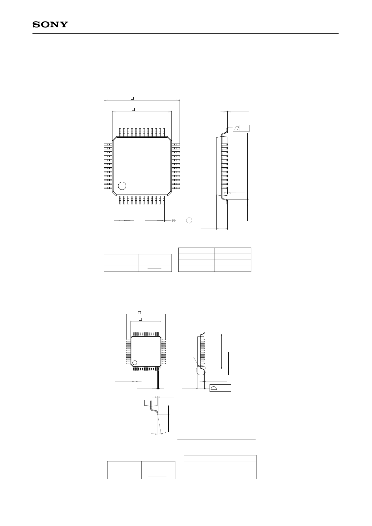
Package Outline Unit: mm
CXA1390AQ
15.3 ± 0.4
+ 0.4
12.0 – 0.1
48PIN QFP (PLASTIC)
+ 0.1
0.15 – 0.05
CXA1390AQ/AR
CXA1390AR
2536
37
48
112
0.8 0.3 – 0.1
SONY CODE
EIAJ CODE
JEDEC CODE
+ 0.15
QFP-48P-L04
∗QFP048-P-1212-B
48PIN LQFP (PLASTIC)
24
13
M
± 0.12
+ 0.35
2.2 – 0.15
PACKAGE STRUCTURE
PACKAGE MATERIAL
LEAD TREATMENT
LEAD MATERIAL
PACKAGE WEIGHT
0.15
+ 0.2
0.1 – 0.1
EPOXY RESIN
SOLDER / PALLADIUM
PLATING
COPPER / 42 ALLOY
0.7g
13.5
0.9 ± 0.2
37
48
0.5 ± 0.08
SONY CODE
EIAJ CODE
JEDEC CODE
∗ 7.0 ± 0.1
36
1
9.0 ± 0.2
+ 0.08
0.18 – 0.03
0° to 10°
DETAIL A
LQFP-48P-L01
∗QFP048-P-0707-A
25
12
24
A
13
(0.22)
+ 0.2
1.5 – 0.1
0.1 ± 0.1
0.5 ± 0.2
NOTE: Dimension “∗” does not include mold protrusion.
0.127 – 0.02
PACKAGE STRUCTURE
PACKAGE MATERIAL
LEAD TREATMENT
LEAD MATERIAL
PACKAGE WEIGHT
(8.0)
0.5 ± 0.2
+ 0.05
0.1
EPOXY / PHENOL RESIN
SOLDER PLATING
42 ALLOY
0.2g
– 17 –
 Loading...