

Page 1

8-bit 75MSPS Flash A/D Converter
CXA1386P/K
Description
The CXA1386P/K are 8-bit high-speed flash A/D
converter ICs capable of digitizing analog signals at
the maximum rate of 75MSPS. The digital I/O levels
of these A/D converters are compatible with the
ECL 100K/10KH/10K.
The CXA1386P/K is pin-compatible with the
earlier models CXA1056P/K, CXA1016P/K,
respectively. They can be replaced by the
CXA1386P/K without any design changes, in most
cases. Compared with the earlier models, these
new models have been greatly improved in
performance, by incorporating advanced process,
new circuit design and carefully considered layout.
Features
• Differential linearity error: ±1/2LSB or less
• Integral linearity error: ±1/2LSB or less
• High-speed operation with maximum conversion
rate of 75MSPS (Min.)
• Wide analog input bandwidth: 150MHz (Min. for
full-scale input)
• Low Power consumption: 580mW (Typ.)
• Single power supply: –5.2V
• Low input capacitance: 17pF (Typ.)
• Built-in integral linearity conpensation circuit
• Low error rate
• Operable at 50% clock duty cycle
• Good temperature characteristics
• Capable of driving 50Ω loads
CXA1386P
28 pin DIP (Plastic)
CXA1386K
44 pin LCC (Ceramic)
Structure
Bipolar silicon monolithic IC
Applications
• Digital oscilloscopes
• HDTV (high-definition TVs)
• Other apparatus requiring high-speed A/D
conversion
Pin Configuration
Pins with name are NC pins (not connected).
LINV
1
DVEE
2
DGND
(LSB) D0
(MSB) D7
DGND
Sony reserves the right to change products and specifications without prior notice. This information does not convey any license by
any implication or otherwise under any patents or other right. Application circuits shown, if any, are typical examples illustrating the
operation of the devices. Sony cannot assume responsibility for any problems arising out of the use of these circuits.
D1
D2
D3
D4
D5
D6
DV
EE
MINV
10
11
12
13
14
3
4
5
6
7
8
9
CXA1386P
26
25
20
19
18
17
16
15
28
27
24
23
22
21
AVEE
RT
V
AVEE
AGND
IN
V
AGND
RM
V
AGND
IN
V
AGND
EE
AV
VRB
CLK
CLK
AV
EE
AVEE
VRT
AVEE
LINV
DV
EE
DGND1
DGND2
RM
39
38 37 36 35 34 33 32 31 30 29
40
41
42
43
44
1
2
3
4
5
6
8 9 10 11 12 13 14 15 16 17
7
IN
AGND
V
CXA1386K
D2
D1
(LSB) D0
V
AGND
D3
D4
AGND
D5
IN
AGND
V
D6
(MSB) D7
28
27
26
25
24
23
22
21
20
19
18
DGND2
EE
AV
AVEE
VRB
CLK
CLK
MINV
DV
EE
DGND1
– 1 –
E90114C54-ST
Page 2

Absolute Maximum Ratings (Ta = 25°C)
• Supply voltage AVEE, DVEE –7 to +0.5 V
• Analog input voltage VIN –2.7 to +0.5 V
• Reference input voltage VRT, VRB, VRM –2.7 to +0.5 V
I VRT – VRB I 2.5 V
• Digital input voltage CLK, CLK, MINV, LINV –4 to +0.5 V
I CLK – CLK I 2.7 V
• VRM pin input current IVRM –3 to +3 mA
• Digital output current ID0 to ID7 –30 to 0 mA
• Storage temperature Tstg –65 to +150 °C
Recommended Operating Conditions Min. Typ. Max. Unit
• Supply voltage AVEE, DVEE –5.5 –5.2 –4.95 V
AVEE – DVEE –0.05 0 +0.05 V
AGND – DGND –0.05 0 +0.05 V
• Reference input voltage VRT –0.1 0 +0.1 V
VRB –2.2 –2.0 –1.8 V
• Analog input voltage VIN VRB VRT
• Pulse width of clock TPW1 6.6 ns
TPW0 6.6 ns
• Operating temperature Tc (CXA1386K) –20 +100 °C
Ta (CXA1386P) –20 +75 °C
CXA1386P/K
– 2 –
Page 3

Block Diagram
CXA1386P/K
MINV
r1
V
RT
Comparator
r/2
r
VIN
VRM
VIN
63
64
65
126
127
128
129
191
192
193
254
1
2
•
•
•
•
•
•
OUTPUT
ENCODE LOGIC
•
•
•
•
•
•
D7 (MSB)
D6
D5
D4
D3
D2
D1
D0 (LSB)
r
r
r
r
r
r
r2
r
r
r
r
r
r
r
VRB
CLK
CLK
r3
r/2
CLOCK
DRIVER
255
LINV
– 3 –
Page 4
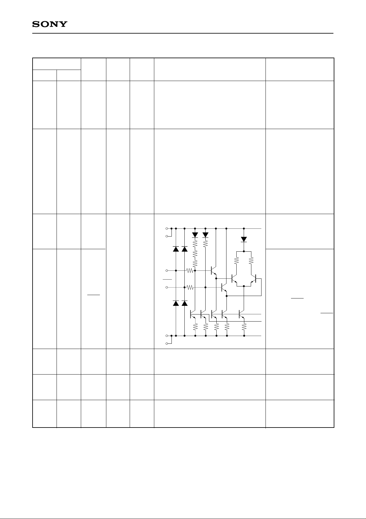
Pin Description and I/O pin Equivalent circuit
CXA1386P/K
Pin No
DIPLCC
31, 33,
35, 37
27, 28,
40, 41,
44
23 CLK
19, 21,
23, 25
18, 26,
28
16
Standard
Symbol I/O
voltage
level
AGND — 0V
AVEE — –5.2V
Equivalent circuit Description
Anlog GND.
Used as GND for input
buffers and latches of
comparators.
Isolated from DGND or
DGND 1/2.
Analog VEE
–5.2V (Typ.).
Internally connected
with DVEE
(resistance: 4 to 6Ω).
Ceramic chip
capacitors of at least
0.1µF should be used
to connect to AGND
and be placed near
the pins.
DGND (DG ND1)
CLK input
22 CLK
15
3, 12— DGND — 0V
—5, 19 DGND1 — 0V
—6, 16 DGND2 — 0V
I ECL
CL K
CL K
DV
EE
r r
r
r
r r
Input complementary
to CLK.
With open connection,
kept at threshold
voltage (–1.3V).
Device is operable
without CLK input, but
use of complementary
inputs of CLK and CLK
is recommended to
obtain the stable highspeed operation.
Digital GND (Used for
internal circuits and
output transistors)
Digital GND (Used for
internal circuits)
Digital GND (Used for
output buffers)
– 4 –
Page 5

CXA1386P/K
Pin No
Symbol I/O
Standard
voltage
DIPLCC
2, 134, 20 DVEE — –5.2V
8D0
9
10
11
4
5
6
7
D1
D2
D3
O ECL
12
13
8
9
D4
D5
level
Equivalent circuit Description
Digital VEE
Internally connected
with AVEE
(resistance: 4 to 6Ω)
Ceramic chip
capacitors of at least
0.1µF should be used
to connect to DGND
and be placed near the
pins.
DGND (DG ND2)
LSB of data outputs.
External pull-down
resistor is required.
Di
Data outputs.
External pull-down
resistors are required.
14
15 D7
3 LINV I ECL
10
11
1
D6
1421 MINV I ECL
DGND (DG ND1)
LINV
or
MIN V
DVEE
MSB of data outputs.
DV
EE
External pull-down
resistor is required.
Input pin for D0 (LSB)
to D6 output polarity
inversion (see output
code table).
r
r
r
–1.3V
With open connection,
kept at "L" level.
Input pin for D7 (MSB)
output polarity
inversion (see output
r
code table).
With open connection,
kept at "L" level.
– 5 –
Page 6
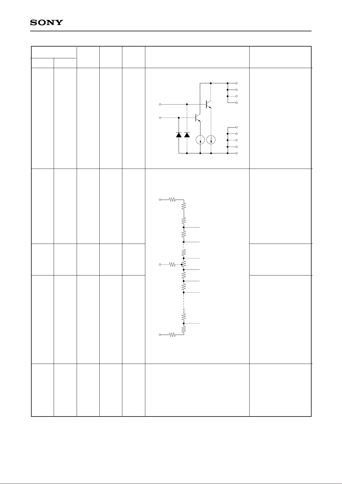
CXA1386P/K
Pin No.
Symbol I/O
DIPLCC
32, 36 VIN I
26 VRB
34
42
20, 24
17
22
27
VRM IVRB/2
VRT I0V
I
Standard
voltage
level
VRT
to
VRB
–2V
VIN
VIN
VRT
VRM
VRB
Equivalent circuit Description
AGND
Analog input pins.
These two pins must
be connected
externally, since they
are not internally
connected.
See Application Note
for precautions.
AVEE
Reference voltage
(bottom)
Typically –2V
r1
r/2
r
Comparator 1
r
Comparator 2
r
r2
3
r
Comparator 127
r
Comparator 128
r
Comparator 129
r
Comparator 130
r
Comparator 255
r/2
A ceramic capacitor of
at least 0.1µF and a
tantalus capacitor of at
least 10µF should be
used to connect to
AGND and be placed
near the pins.
•
Reference voltage mid
•
•
point be used as a pin
for integral linearity
compensation
Reference voltage
(top) Typically 0V
When a voltage
•
•
different from AGND is
•
•
applied to this pin, a
•
•
ceramic capacitor of at
•
least 0.1µF and a
tantalus capacitor of at
least 10µF should be
used to connect to
AGND and be placed
near the pins.
1, 2,
7, 17,
18, 24,
25, 29,
30, 38
39, 43
NC — —
Unused pins
No internal connections
have been made to
these pins.
Connecting them to
AGND or DGND on PC
board is recommended.
– 6 –
Page 7
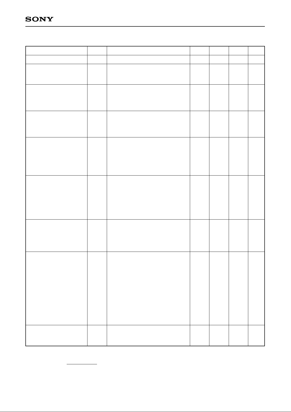
CXA1386P/K
Electrical Characteristics (Ta = 25°C, AVEE = DVEE = –5.2V, VRT = 0V, VRB = –2V)
Item
Resolution
DC characteristics
Integral linearity error
Differential linearity error
Analg input
Analog input capacitance
Analog input resistance
Input bias current
Reference inputs
Reference resistance
Offset voltage VRT
VRB
Digital inputs
Logic H level
Logic L level
Logic H current
Logic L current
Input capacitance
Switching characteristics
Maximum conversion rate
Aperture jitter
Sampling delay
Output delay
H pulse width of clock
L pulse width of clock
Symbol Condition Min. Typ. Max. Unit
n
EIL
EDL
CIN
RIN
IIN
RREF
EOT
EOB
VIH
VIL
IIH
IIL
Fc
Taj
Tds
Tdo
TPW1
TPW0
Fc = 75MSPS
Fc = 75MSPS
VIN = –1V + 0.07Vrms
VIN = –1V
Input connected to –0.8V
Input connected to –1.6V
Error rate 10–9TPS
∗1
75
8
0
–1.13
0
–50
75
4.0
6.6
6.6
8
±0.3
±0.3
17
390
110
18
10
7
10
3.0
6.5
±0.5
±0.5
200
155
32
24
–1.50
50
50
9.0
bits
LSB
LSB
pF
kΩ
µA
Ω
mV
mV
V
V
µA
µA
pF
MSPS
ps
ns
ns
ns
ns
Digital outputs
Logic H level
Logic L level
Output rising time
Output falling time
Dynamic characteristics
Input bandwidth
S/N ratio
Error rate
Differential gain error
Differential phase error
Power supply
Supply current
Power consumption
∗1
TPS: Times Per Sample
∗2
Pd = IEE · VEE +
(VRT – VRB)
∗2
RREF
VOH
VOL
Tr
Tf
DG
DP
IEE
Pd
2
RL = 620Ω to DVEE
RL = 620Ω to DVEE
RL = 620Ω to DVEE, 20% to 80%
RL = 620Ω to DVEE, 80% to 20%
VIN = 2Vp-p
Input frequency at –3dB
Input = 1MHz, FS
{
Clock = 75MHz
Input = 18.75MHz, FS
{
Clock = 75MHz
Input = 18.749MHz, FS
Error > 16LSB
{
Clock = 75MHz
NTSC 40IRE mod. ramp,
}
Fc = 75MSPS
–1.03
150
–150
0.9
2.1
46
40
1.0
0.5
–104
580
–1.62
–9
10
V
V
ns
ns
MHz
dB
dB
TPS
%
deg
mA
mW
∗1
– 7 –
Page 8

Output Code Table
CXA1386P/K
∗
VIN
Step
0V
0
1
–1V
127
128
254
255
–2V
∗
VRT = 0V, VRB = –2V
Timing diagram
MINV 1
LINV 1
0
1
1
0
0
0
D7 D0 D7 D0 D7 D0 D7 D0
0 0 0 ······ 0 0
0 0 0 ······ 0 0
0 0 0 ······ 0 1
:
:
0 1 1 ······ 1 1
1 0 0 ······ 0 0
:
:
1 1 1 ······ 1 0
1 1 1 ······ 1 1
1 1 1 ······ 1 1
1 0 0 ······ 0 0
1 0 0 ······ 0 0
1 0 0 ······ 0 1
:
:
1 1 1 ······ 1 1
0 0 0 ······ 0 0
:
:
0 1 1 ······ 1 0
0 1 1 ······ 1 1
0 1 1 ······ 1 1
0 1 1 ······ 1 1
0 1 1 ······ 1 1
0 1 1 ······ 1 0
:
:
0 0 0 ······ 0 0
1 1 1 ······ 1 1
:
:
1 0 0 ······ 0 1
1 0 0 ······ 0 0
1 0 0 ······ 0 0
1 1 1 ······ 1 1
1 1 1 ······ 1 1
1 1 1 ······ 1 0
:
:
1 0 0 ······ 0 0
0 1 1 ······ 1 1
:
:
0 0 0 ······ 0 1
0 0 0 ······ 0 0
0 0 0 ······ 0 0
Analog input
CLK
CLK
Digital output
Tdo
Tds
20%
N + 1
80%
Tr Tf
NN – 1
80%
N + 2
N + 1
20%
N
Tpw0Tpw1
– 8 –
Page 9
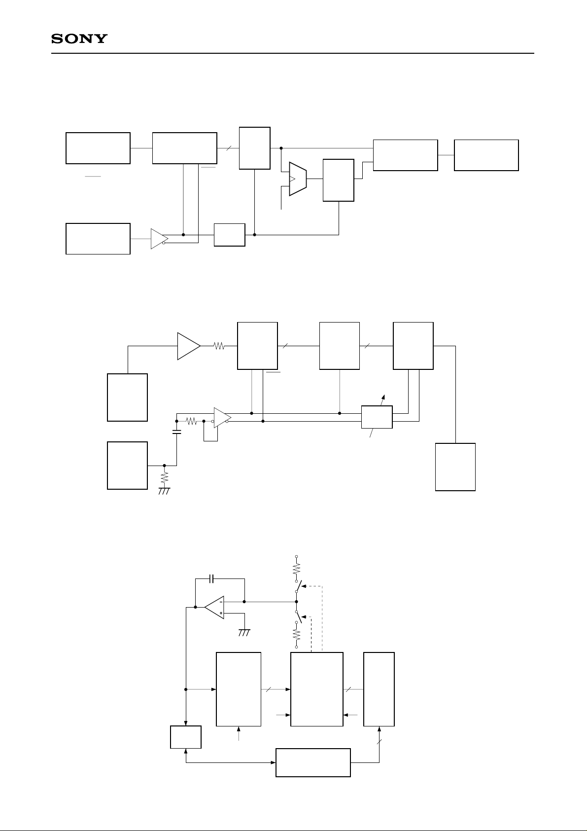
Electrical Characteristics Test Circuit
Maximum conversion rate test circuit
CXA1386P/K
Signal
Source
fCLK
– 1kHz
4
2Vp-p Sin Wave
Signal
Source
f
CLK
Vin
CXA1386
P/K
CLK
CLK
Differential gain error test circuit
Differential phase error test circuit
Amp
NTSC
Signal
Source
V
10Ω
8
1/4
IN
ECL
Latch
DAT A 16
DUT
CXA1386
P/K
CLK CLK
+
8 8
ECL
Latch
ECL
Latch
A
B
Delay
Comparator
A > B
(CX20202A-1)
10bit
D/A
Pulse
Counter
SG (CW)
50
Integral linearity error test circuit
Differential linearity error test circuit
IN
V
DVM
VBB
DUT
CXA1386
P/K
CL K (75MHz)
+V
S2
S1: ON when A < B
S2: ON when A > B
S1
–V
A < B A > B
8 8
Comparator
A8
B8
to
to
A1
B1
A0
B0
Controller
Vector
Scope
DG.DP
Buffer
"1""0"
00000000
8
to
11111110
– 9 –
Page 10

Power Supply Current Test Circuit
Analog input bias current test circuit
10
11
12
13
14
1
2
3
4
5
6
7
8
9
CXA1386P
28
27
26
25
24
23
22
21
20
19
18
17
16
15
–1V
A
–2V
CXA1386P/K
I
IN
I
–1V
IN
A
39
38 37 36 35 34 33 32 31 30 29
40
41
42
43
44
1
2
3
4
5
6
8 9 10 11 12 13 14 15 16 17
7
IEE
A
CXA1386K
28
27
26
25
24
23
22
21
20
19
18
–2V
A
IEE
–5.2V
Sampling delay test circuit
Aperture jitter test circuit
37.5MHz
Amp
OSC1
φ: Variable
IN
fr
OSC2
37.5MHz
V
CLK
ECL
Buffer
CXA1386
P/K
–5.2V
Aperture jitter test method
0V
VIN
CLK
8
Logic
Analizer
VIN
1024
samples
CLK
Aperture jitter is defined as follows:
∆v
∆t
129
128
t
127
126
125
Aperture jitter
–1V
–2V
σ (LSB)
Taj = σ/ = σ/( ),
Where σ (unit: LSB) is the deviation of the output codes when the input
frequency is exactly the same as the clock and is sampled at the
largest slew rate point.
∆υ
∆t
256
2
× 2πf
– 10 –
Page 11
CXA1386P/K
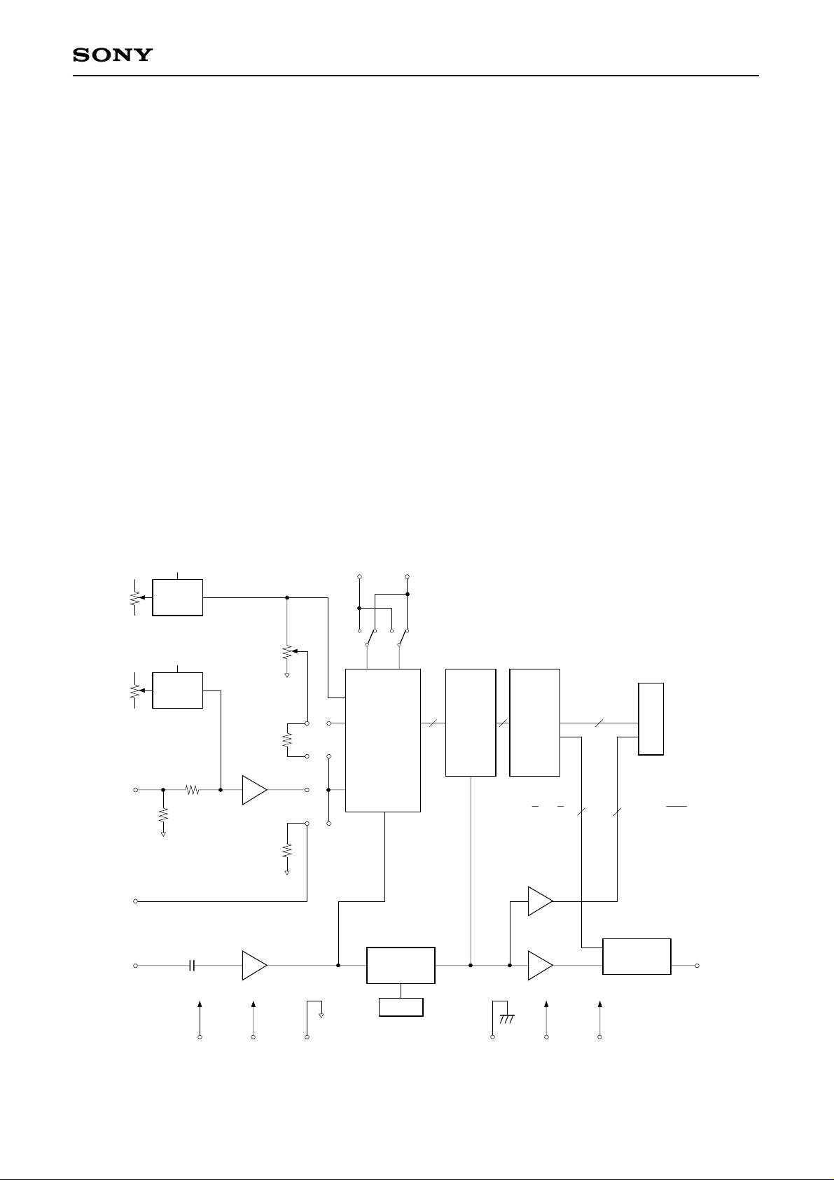
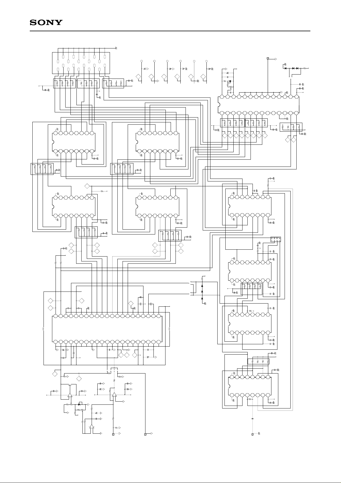
8bit 75MSPS ADC and DAC Evaluation Board
It is necessary to equip "the CXA1396D/P EVALUATION BOARD WITH DAC" with "A1396D – A1386P
ADAPTER" in order to evaluate CXA1386P.
In addition to indispensable features such as the reference voltage generator, this tool equips two sets of
analog inputs (the direct input and the buffer amplifier input), the input voltage offset generator, the clock
decimator, the output data latches, the 10-bit high-speed DAC, and the 20-pin cable connector for digital
outputs. This evaluation board provides full performance of the CXA1386P and it is designed to facilitate
evaluation.
Features
Resolution: 8bits
Maximum conversion rate: 75MSPS
Supply voltage: +5.0V, –5.2V, –2.0V
Two analog inputs (Direct input, buffer amplifier input)
Clock level converter: Sine wave to ECL level signal
Reference voltage adjustment circuit for the A/D converter
Built-in clock frequency decimation circuit: (1/1 to 1/16)
Fig. 1. Block Diagram
–5.2V (A)
V
(2k)
V
(2k)
AMP.IN
DIR.IN
R2
R1
VRB
–2V
–5.2V (A)
Vin
OFFSET
240
51
X (–2)
V
(1k)
LH
R3
1k
51
SW1 SW2
LINV MINV
V
J1
A
B
C
D
RB
VRM
CXA1386P
Vin
CLK
DIGITAL OUT
(CONNECTOR)
(D7 to D0)
8
8
2 (CLK.CLK)
CLK
8
BUFFER
(D7 to D0)
8
DATA
LATCH
CLK
0.1µ
DECIMATOR
SW3
1/1 to 1/16
– 11 –
D/A
CONVERTER
CLK
–5.2V (D) DGND –2V (D)–5.2V (A) AGND+5V
D/A OUT
Page 12
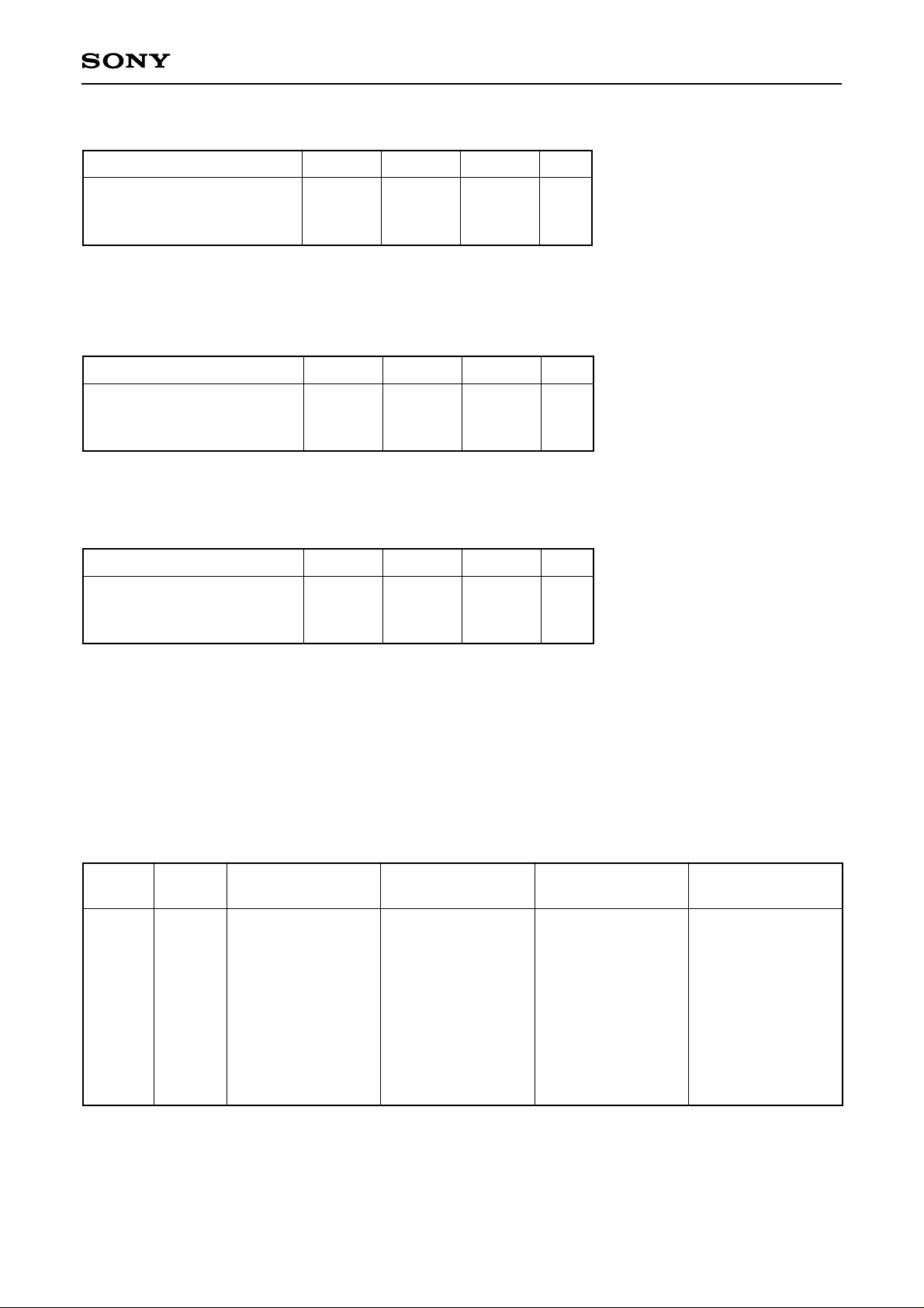
Supply Current
Item Min. Typ. Max. Unit
–5.2V
+5.0V
–2.0V
0.85
15
0.45
1.0
30
0.6
A
mA
A
(Note: Supply current –2.0V is the value when Rn10, Rn11 and Rn12 are not mounted.)
Analog Input (DIR. IN, AMP. IN)
Item Min. Typ. Max. Unit
Input voltage (DIR. IN)
(AMP. IN)
Input impedance
∗1
–2.0
–0.5
50
0
+0.5
V
V
Ω
(∗1: Adjustable by VR1)
CXA1386P/K
Clock Input (CLK)
Item Min. Typ. Max. Unit
Input voltage
(Peak to Peak)
Input impedance
Digital Output (D0 to D7)
ECL 10KH level
Clock Output
ECL 10KH level, complementary output
Output Code Table
VIN
MINV
LINV
0V
:
:
:
:
:
:
:
:
–2V
0
0
1 1 1 ······ 1 1
1 1 1 ······ 1 0
:
:
1 0 0 ······ 0 0
0 1 1 ······ 1 1
:
:
0 0 0 ······ 0 1
0 0 0 ······ 0 0
2.0
50
0
1
1 0 0 ······ 0 0
1 0 0 ······ 0 1
:
:
1 1 1 ······ 1 1
0 0 0 ······ 0 0
:
:
0 1 1 ······ 1 0
0 1 1 ······ 1 1
Vp-p
Ω
1
0
0 1 1 ······ 1 1
0 1 1 ······ 1 0
:
:
0 0 0 ······ 0 0
1 1 1 ······ 1 1
:
:
1 0 0 ······ 0 1
1 0 0 ······ 0 0
1
1
0 0 0 ······ 0 0
0 0 0 ······ 0 1
:
:
0 1 1 ······ 1 1
1 0 0 ······ 0 0
:
:
1 1 1 ······ 1 0
1 1 1 ······ 1 1
– 12 –
Page 13
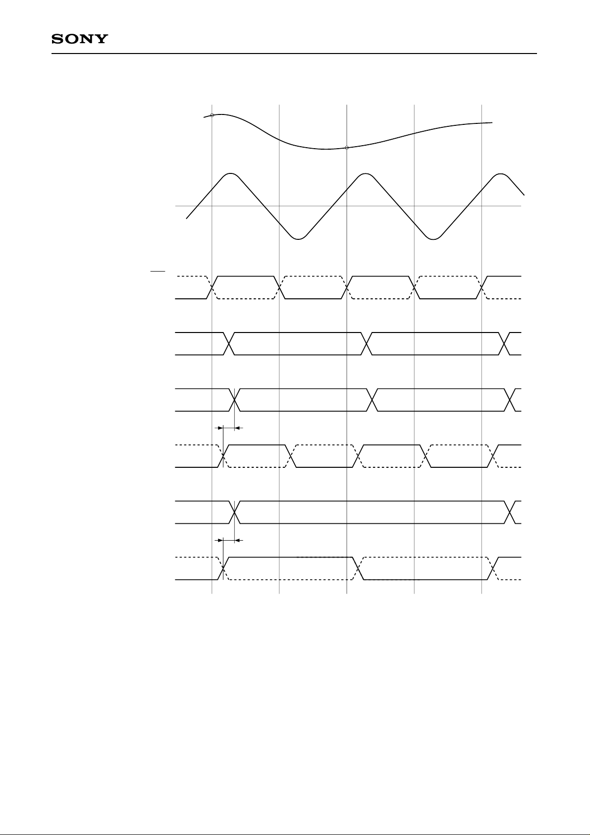
Fig. 2. Timing Chart
A/D input pin
(DIR. IN, AMP. IN)
CXA1386P/K
N
Vin
N + 1
PCB input pin
A/D clock
A/D output
PCB output pin
(For 1/1 frequency division)
PCB output pin
(For 1/1 frequency division)
D7 to D0
D7 to D0
CLKN
CLK
CLK
CLK
N – 1 N
N – 2 N – 1 N
Tdh
1.8ns
(Typ)
CLK
PCB output pin
(For 1/2 frequency division)
PCB output pin
(For 1/2 frequency division)
DATA OUT
CLKN
CLK
N – 2N – 4
Tdh
1.8ns
(Typ)
Adjustment Methods and Notes on Operation
1) Vin Offset (VR1)
The volume to adjust the signal range (0V center assumed) with the A/D converter input range when a
waveform is input through AMP. IN.
2) A/D Full Scale (VR2)
The volume to adjust A/D converter VRB voltage.
3) Linearity (VR3)
The volume to adjust VRM (linearity) voltage.
– 13 –
N
Page 14
4) D/A Full Scale (VR4)
The volume to adjust D/A output full scale (–1V)
CXA1386P/K
5) J1 (input selection)
A: Shorts to adjust VRM voltage.
B: Shorts to supply DC voltage to Vin.
C: Shorts to select AMP.IN input.
D: Shorts to select DIR. IN input.
6) SW1
The switch for LINV High/Low
7) SW2
The switch for MINV High/Low
8) SW3 (Decimation)
The switch to select clock frequency decimation.
Switch position: decimation ratio
0: 1/1
1: 1/2
2: 1/4
3: 1/8
4: 1/16
[Jumper Poisition at shipment]
J1
A
B
C
D
9) SW4 (D/A INV)
The switch for D/A converter output inversion.
10) Rn10, Rn11 and Rn12 are not mounted at shipment. They are not required during evaluation.
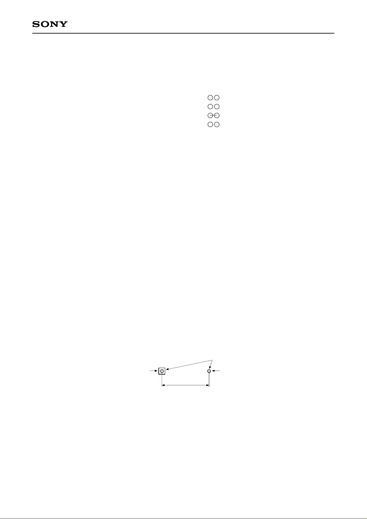
11) Waveform probe pins P5 and P8 through P28 are devised to facilitate GND connection in order to reduce
the distortion. As shown in the diagram below, the distance between the probe point and the GND is 300
mils, and there is φ1.2mm throughhole at each. The signal and GND locations are suit for a Tektronix GND
tip (part number 013-1185-00).
φ1.2mm
Probe pointGND
300mil
Fig. 3.
12) D/A converter (IC13) input data (waveform probe pins P21 through P28) are the complementary signals of
the decimated A/D converter outputs. Those are inverted again in the D/A converter so that the direction of
reproduced waveform can agree with the A/D input signal converter.
13) The part number of the digital output connector is KEL 8830E-020-170S. A corresponding connector and
cable assembly is JUNKOSHA KB0020MCG50BI.
– 14 –
Page 15
CXA1386P/K
8
4
DGND
2
(TOP VIEW)
CONNECTOR
1
KEL: 8830E-020-170S
51
Rn12
–2V (D)
DGND
C53
0.1µ
16
CC2
V
CC1
V
1
C42
Rn675Rn675Rn6
0.1µ
75
–2V (D)
Rn6
75
Rn6
16
VCC2
VCC1
1
R1751R16
CLKN
P8
CLK
P9
21
CLK
BEAD
FERRITE
NC
22
P2
VRB
C9
0.1µ
+5V (A)
DGND
6
DGND
DGND
3
7
D1
D3
5
D0
D2
51
Rn12
Rn1251Rn1251Rn12
DGNDDGND
14
13
15
12
Din
COM
Dout_
Cout_
Aout_
Bout_
Ain
Aout
3
2
5
4
DGND
DGND
14
12
13
15
D5D4D3
Q5Q4Q3
Q0Q1Q2D0D1D2V
4
3
2
5
DGND
Rn4
DGND
P17
P16
C22
0.1µ
D6 D7
–2V (D)
51
C25
0.1µ
C27
0.1µ
20
19
17
18
EE
NC
DV
MINV
CLKN
VRBNCAVEEAVEENCNC
25
24
26
23
AGND
AGND
10
C20
C19
0.1µ
C18
0.1µ
Linearity
AGND
1k
VR3
Q1
IC1-2
2SA970
TL4558
7
AGND
4
8
6
5
IC3
TL431CP
2k
R8
R9
VR2
1.3k
R6
AGND
A/D Full Scale
12
DGND
10
DGND
DGND
11
D5
9
D6
13 14
D4
51
51
Rn11
Rn11
Rn11
9
11
10
IN
Cin
Cout
Dout
IC12 : 10H101
EE
Bout
Bin
V
6
8
7
C41
0.1µ
P18
CLK
9
11
10
CLK
IC10 : 10H176
EE
8
7
6
75
Rn475Rn475Rn4
Rn4
–5.2V (D)
EE
P17
DV
DGND
14
16
15
D7D6D5D4D3D2D1
DGND1
DGND2
AGND
28
27
29
–5.2V (A)
P1
VRM
C8
0.1µ
AGND
+5V (A)
–5.2V (A)
AGND
2K
510
VR1
1k
R7
240
Vin Offset
R4
22k
1
R5/11k
6
–5.2V (A)
2
3
16
DGND
18
15
D7
17
51
51
Rn11
Rn11
C52
0.1µ
–5.2V (D)
DGND
R19
C26
C36
75
P15P14
13
VIN
30
AGND
C12
C7
C4
3.3µ
C3
0.1µ
4
IC1-1
TL4558
Fig. 4. PCB Circuit Schematic
DGND
CLK
–2V (D)
DGND
51
0.1µ
0.1µ
D4 D5
12
AGND
31
0.1µ
1µ
AGND AGND
AGND
20
DGND
19
CLKN
Rn10
–5.2V (D)
–2V (D)
11
VRM
32
A
1k
R13
AGND AGND
DIGITAL OUT
75
Rn10
Rn5
–2V (D)
DGND
DGND
AGND
C17
0.1µ
B
43
R11
510
R10
7
2
R2
240
75
Rn10
Rn5
10
33
C
6
3
R1
AMP.IN
DGND
75
75
9
VIN
34
AGND
D
J1
IC4
CLC404AJP
4
51
Rn10
P5
VIN
R12
C6
+5V (A)
AGND
+5V (A)
33µ
C57
P34
C51
0.1µ
DGND
75
Rn10
–2V (D)
DGND
15
16
VCC2
Dout_
VCC1
Aout_
2
1
DGND
C40
0.1µ
DGND
75
Rn575Rn575Rn5
8
CXA1396D – CXA1386P ADAPTER
AGNDNCNC
35
AGND
51
1µ
AGND
AGND
AGND
AGND
7
D0
36
P4
C11
0.1µ
DGND
P6
DGND2
AGND
–5.2V (A)
6
37
AGND
AGND
P3
EE
AV
16
VCC2
VCC1
1
1µ
C26
C25
0.1µ
DGND
5
DGND1
AVEEAVEENCVRT
38
–2V (D)
DGND
15
Q5Q4Q3
Q0Q1Q2D0D1D2V
2
DGND
–5.2V (D)
4
EE
DV
39
C16
–5.2V (A)
C15
DIR.IN
3
LINV
40
0.1µ
14
Cout_
Bout_
3
14
3
C24
1µ
AGND
P33
D3
D2
23
6
Rn875Rn8
P23
C37
12
Cin_
IC8 : 10H116
Ain
5
C31
R18
12
IC7 : 10H164
5
51
12
D0
IC5 : 10H136
5
12
Cin_
IC2 : 10H116
Ain
5
51
CLK
22
7
0.1µ
V
0.1µ
51
X4
–2V (D)
D1
51
V
P22
DGND
11
BB
Bout_
6
11
6
11
6
Rn151Rn1
11
BB
Bout_
6
D/A OUT
21
20
OUT
IC13 : CX20202A-1
9
8
75
75
Rn8
Rn8
P21
D0
C38
51
R20
9
10
Bin
Bin_
EE
Bout
V
8
7
C34
DGND
C30
–2V (D)
C29
9
10
B
C
EE
8
7
C22
0.1µ
51
C21
0.1µ
C37
9
10
S1
Cin_
EE
8
7
C14
0.1µ
C13
0.1µ
C10
0.1µ
51
Rn1
9
10
Bin
Bin_
EE
Bout
V
8
7
C2
0.1µ
DGND
AGND
19
NC
LSBNCNC
10
–2V (D)
DGND
C44
0.1µ
0.1µ
DGND
–2V
(D)
–5.2V (D)
DGND
0.1µ
0.1µ
DGND
0.1µ
DGND
–5.2V (D)
DGND
DGND
0.1µ
DGND
–5.2V (D)
DGND
DGND
DGND
(D)
–2V
C5
0.1µ
(D)
–5.2V
DGND
AGND
18
AGND1
11
Rn7
SW3
DGND
DGND
D4
SW4
D/A INV
DGND
17
DGND
12
51
Rn7
Decimation
L
DGND
P20
CLKN
51
16
INV
CLKN
13
H
–5.2V (D)
D6
D5
R23
3.2k
C47
0.1µ
DGND
C46
0.1µ
DGND
15
–5.2V (D)
EE
DV
CLK
14
51
51
Rn7
Rn7
Rn7
–2V (D)
DGND
C43
0.1µ
P19
CLK
AGND
–5.2V (A)
AGND
–5.2V (A)
33µ
C56
P32
AGND
12
IN
COM
IC11 : 10H101
Aout
5
12
D5D4D3
IC9 : 10H176
5
75
Rn3
1
EE
AV
NC
42
11
Cout
Bout
6
11
6
9
10
Cin
Dout
EE
Bin
V
8
7
C39
0.1µ
9
10
CLK
EE
8
7
C24
0.1µ
Rn375Rn375Rn3
–5.2V (A)
FERRITE BEAD
13
Din
Ain
4
13
4
Rn3
P13
P12
0.1µ
2
NC
41
AGND
AGND
–5.2V (D)
–5.2V (D)
P31
75
33µ
C55
–5.2V (D)
DGND
–5.2V (D)
DGND
C35
0.1µ
D1
P11
D0
P10
DGND
SW2
SW1
DGND
P30
–2V (D)
MINV
LINV
DGND
DGND
DGND
R15
–2V (D)
AGND
33µ
C50
DGND
–2V (D)
33µ
C54
C49
–5.2V (D)
LH
DGND
–2V (D)
0.1µ
240
R22
Rn9
DGND
C45
0.1µ
P29
330
D3D2D1
–5.2V (A)
IC14
TL431CP
1k
R21
2k
VR4
D/A Full Scale
C48
0.1µ
27
28
REF
V
AGND2
MSBD2D3D4D5D6D7D8D9
2
1
75
Rn9
P28
D7D6D5D4D3D2D1
–2V (D)
24
25
26
NCNCNCNCNC
AVEE
4
3
5
75
75
75
Rn9
Rn9
Rn8
Rn9
P24
P26
P25
P27
DGND
16
14
13
15
Cin
Cout
VCC2
Cout_
VCC1
Aout_
Aout
Ain_
2
1
4
3
DGND
DGND
16
14
13
15
Z
X7X6X5
VCC1
VCC
Enable_X3X2X1X0AV
1
4
3
2
Rn2
DGND
Rn251Rn251Rn251Rn2
C23
0.1µ
DGND
DGND
16
14
13
15
Q1
Q0
CLK
VCC2
VCC1
Q2Q3Cout_D3D2S2V
1
4
3
2
DGND
16
14
13
15
Cin
Cout
VCC2
Cout_
VCC1
Aout_
Aout
Ain_
2
1
4
3
DGND DGND
C1
75
R14
Rn151Rn1
R3
0.1µ
– 15 –
Page 16
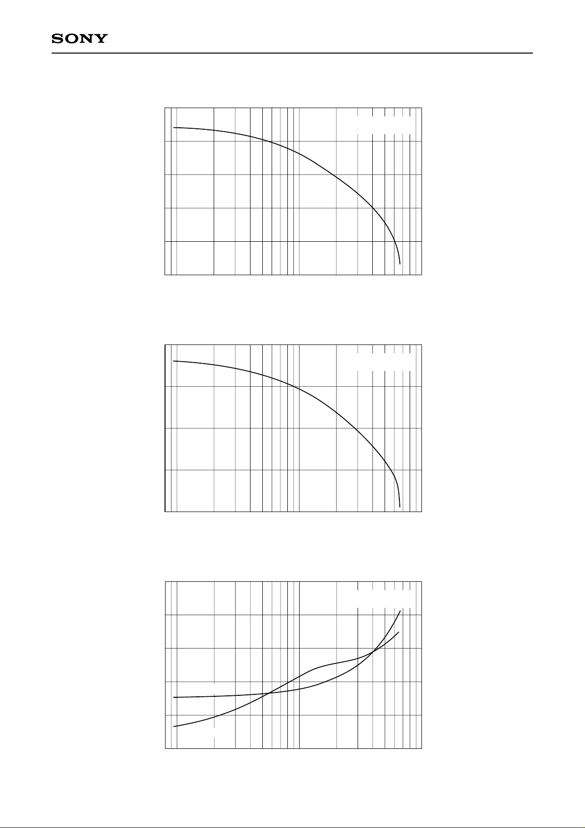
Characteristics Graphs
SNR [dB]
CXA1386P/K
Fig 5. CXA1386P SNR vs. Input Frequency
50
CLK = 75MHz,
VEE = –5.2V
45
40
35
30
25
Fig. 6. CXA1386P Effective Bits vs. Input Frequency
8.0
7.0
6.0
Effective Bits [bit]
5.0
4.0
100101
Input Frequency [MHz]
CLK = 75MHz,
VEE = –5.2V
100101
Input Frequency [MHz]
Fig. 7. CXA1386P 2nd, 3rd Harmonic Distortion vs. Input Frequency
–20
CLK = 75MHz,
VEE = –5.2V
–30
–40
–50
–60
2nd, 3rd Harmonic Distortion [dB]
–70
2nd Hmnc
3rd Hmnc
Input Frequency [MHz]
– 16 –
100101
Page 17
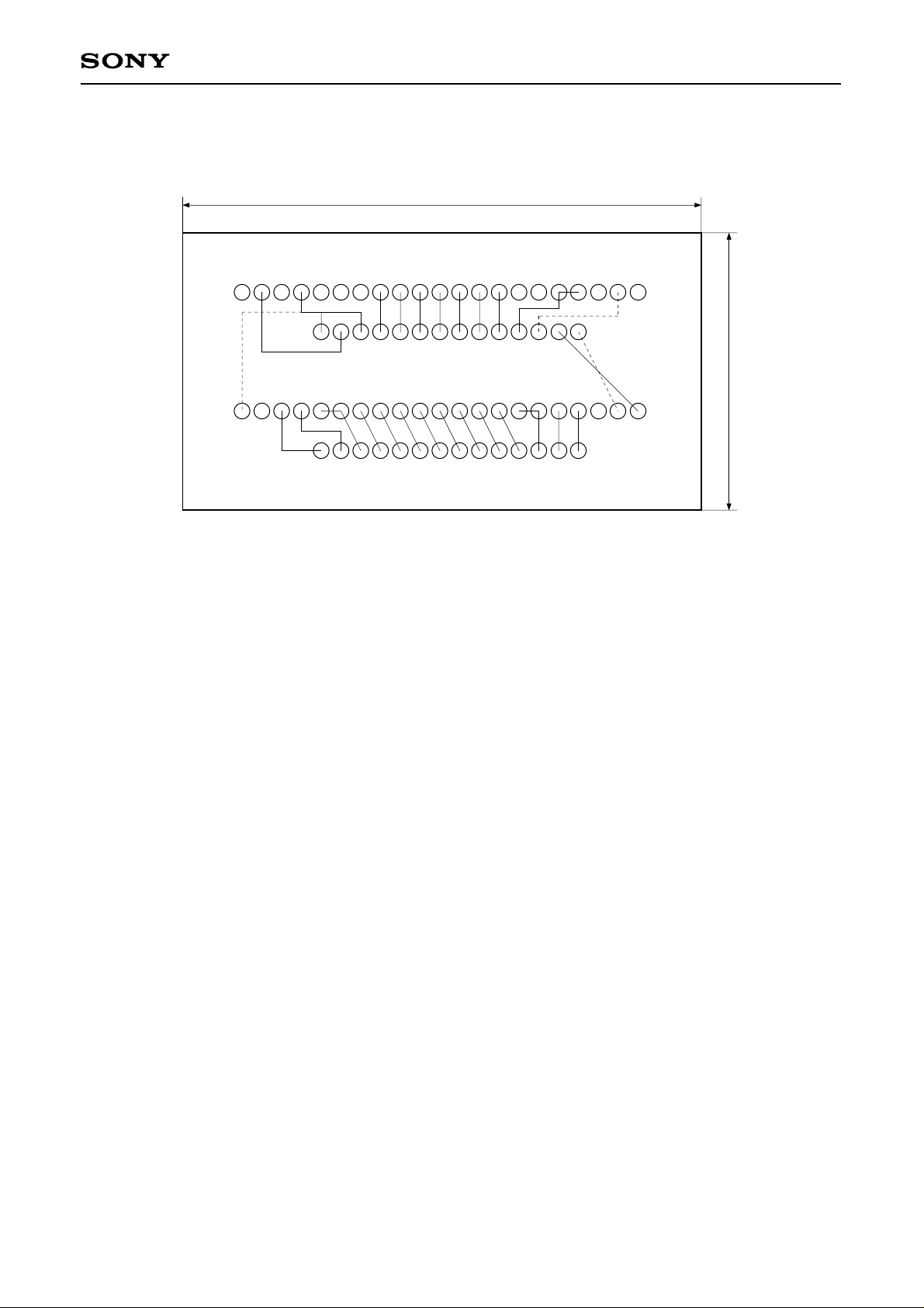
CXA1396D – CXA1386P ADAPTER (SCALE = 2/1)
55mm
CXA1386P ADAPTER
28 15
CXA1386P/K
35mm
141
TOP VIEW
– 17 –
Page 18
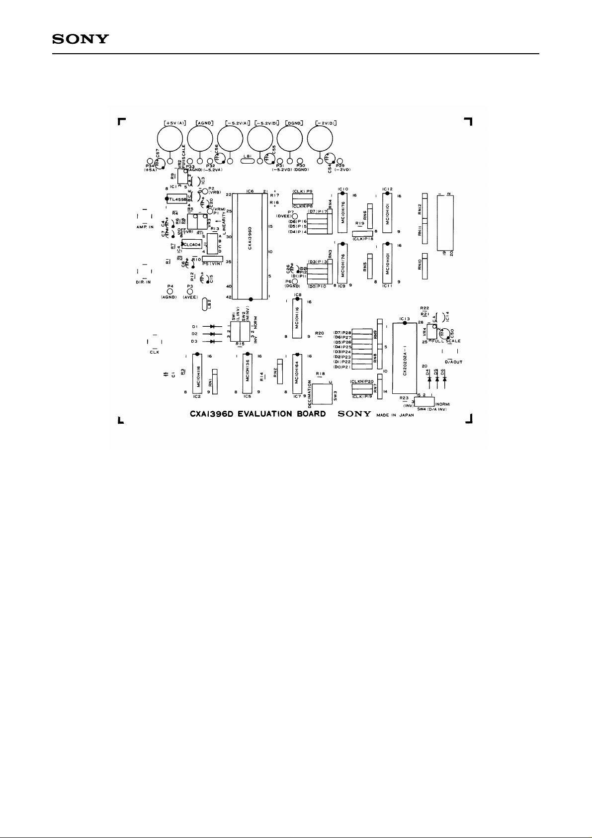
Parts Layout
CXA1386P/K
– 18 –
Page 19
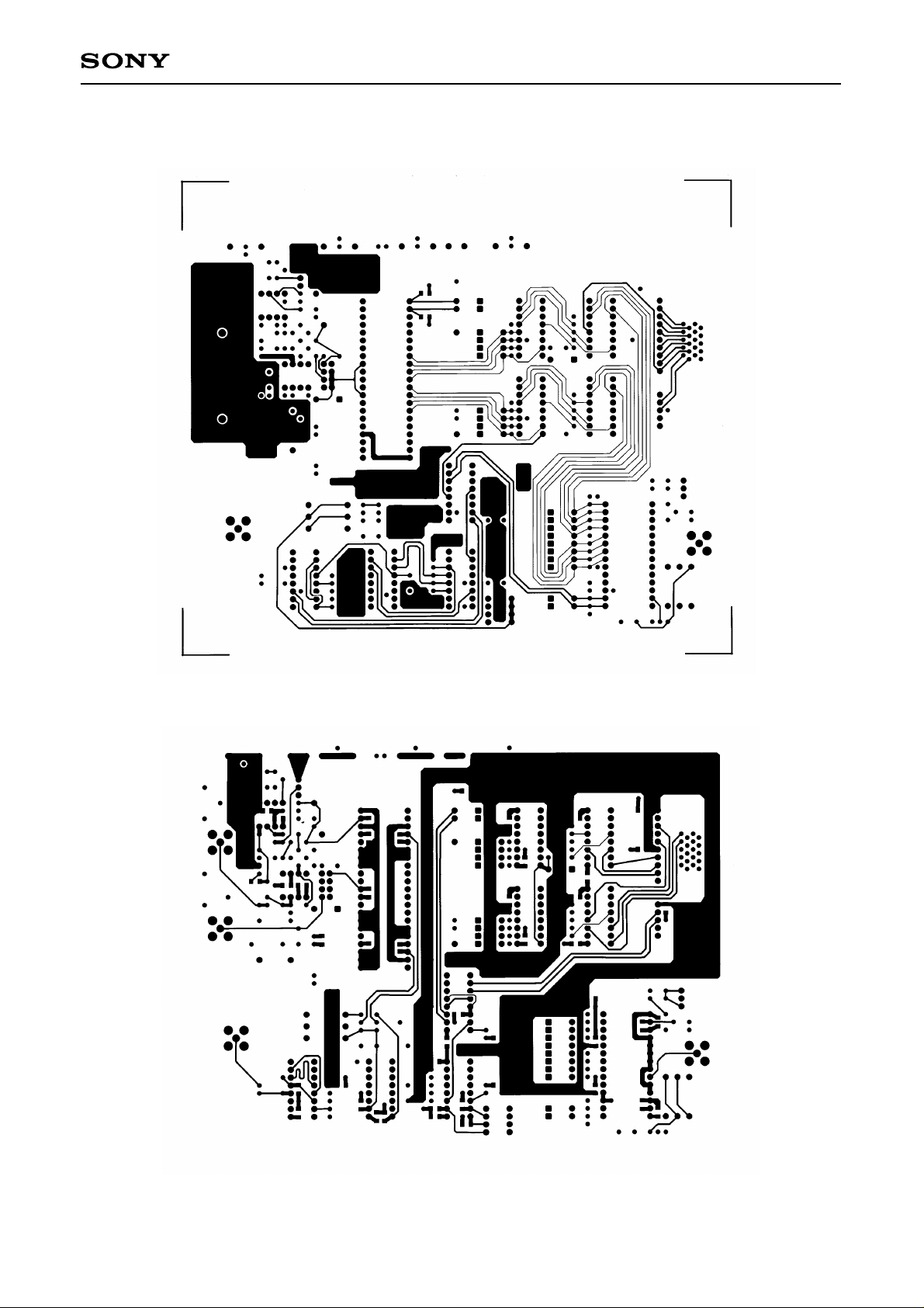
Printed Pattern
CXA1386P/K
1st layer Component plane (Top View)
4th layer Solder plane (Top view)
– 19 –
Page 20
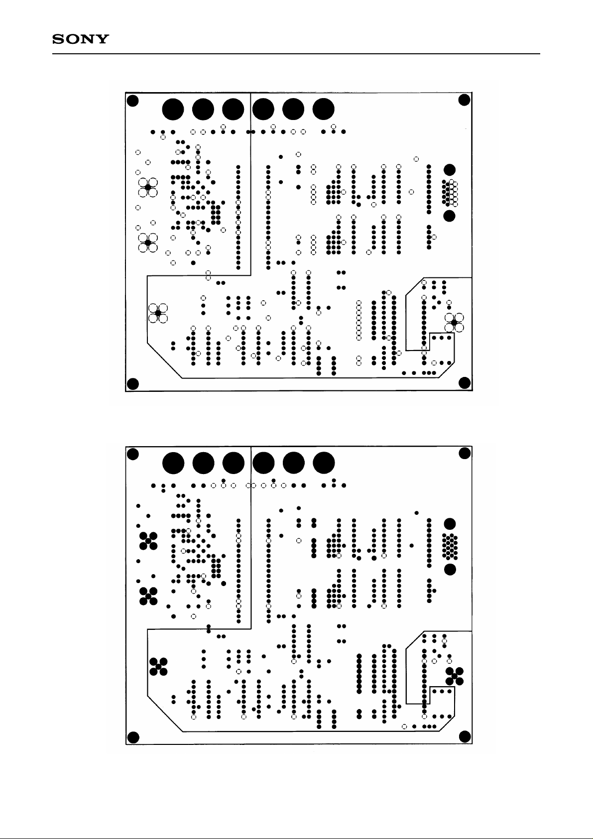
CXA1386P/K
2nd layer GND plane (Top View)
3rd layer Power supply plane (Top View)
– 20 –
Page 21
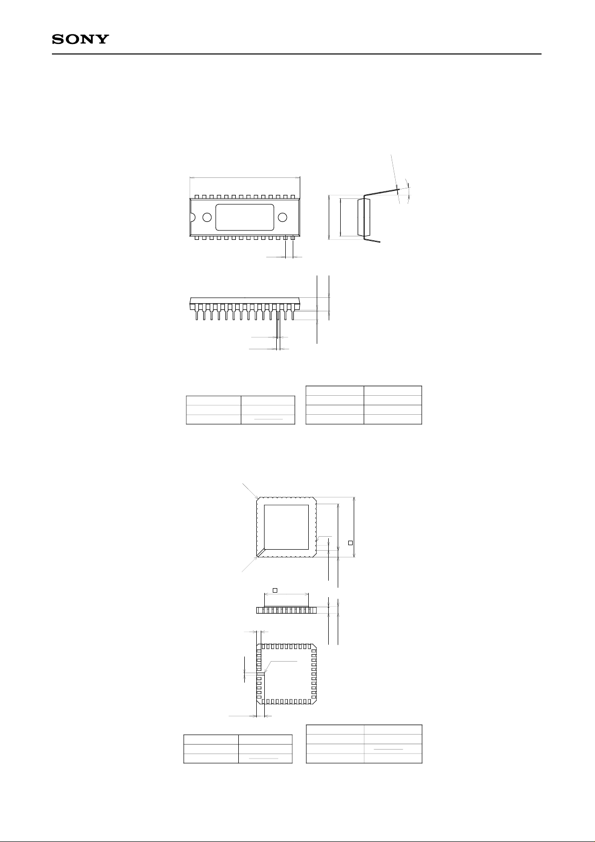
Package Outline Unit: mm
CXA1386P
CXA1386P/K
28PIN DIP (PLASTIC) 600mil
CXA1386K
+ 0.4
37.8 – 0.1
28 15
+ 0.3
15.24
13.0 – 0.1
114
0.5 ± 0.1
1.2 ± 0.15
2.54
+ 0.4
0.5 MIN
3.0 MIN
4.6 – 0.1
PACKAGE STRUCTURE
SONY CODE
EIAJ CODE
JEDEC CODE
DIP-28P-03
∗DIP028-P-0600-C
PACKAGE MATERIAL
LEAD TREATMENT
LEAD MATERIAL
PACKAGE WEIGHT
EPOXY RESIN
SOLDER PLATING
COPPER
4.2g
+ 0.1
0.25 – 0.05
0° to 15°
SONY CODE
EIAJ CODE
JEDEC CODE
44PIN LCC (CERAMIC) 1.8g
C1.016
C0.508
12.5 ± 0.2
1.27
PIN NO.1
0.635 ± 0.07
2.159 ± 0.5
LCC-44C-01
∗QFN044-C-S650-A
INDEX
+ 0.35
12.7 ± 0.1
R0.2
1.27 ± 0.1
0.3
1.651 ± 0.18
16.51 – 0.25
1.905 ± 0.25
1.951 ± 0.25
PACKAGE STRUCTURE
PACKAGE MATERIAL
LEAD TREATMENT
LEAD MATERIAL
PACKAGE WEIGHT
CERAMIC
GOLD PLATING
1.8g
– 21 –
 Loading...