

Page 1
CXA1100P, CXA1101P/M, CXA1102P/M, CXA1163P/M
For the availability of this product, please contact the sales office.
Dolby∗B Type Noise Reduction System
Description
CXA1100, CXA1101, CXA1102 and CXA1163 are
ICs including two separate Dolby B type noise
reduction processors. Seven devices with four Dolby
levels and two types of package are provided for
various applications. These devices feature very few
external components, which is achieved by
integrated filter circuits using integrated thin film
capacitors with high capacitance.
Features
• Minimum number of external components
• NR ON/OFF and REC/PB switchs included
• Small package (DIP16, SOP16)
• Small supply current (
• Dual channel processors in one chip
~
5.5mA, Typ.)
—
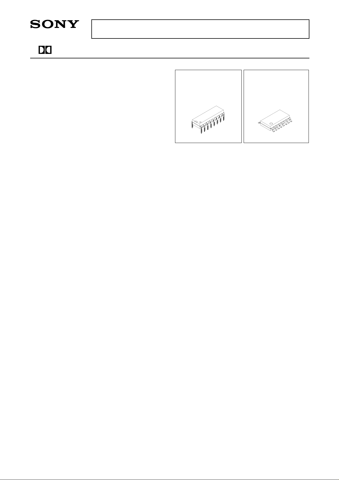
16 pin DIP (Plastic) 16 pin SOP (Plastic)
Absolute Maximum Ratings (Ta = 25°C)
• Supply voltage VCC 17 V
• Operating temperature Topr –30 to +85 °C
• Storage temperature Tstg –55 to +150 °C
• Allowable power dissipation PD
DIP16 (A1100P/A1101P/A1102P/A1163P)900 mW
SOP16 (A1101M/A1102M/A1163M) 500 mW
Note 1) These ICs are available only to the
licensees of Dolby Laboratories Licensing
Corporation from whom licensing and
application information may be obtaind.
Note 2) "Dolby" and double D symbols are trade
marks of Dolby Laboratories Licensing
Corporation.
Sony reserves the right to change products and specifications without prior notice. This information does not convey any license by
any implication or otherwise under any patents or other right. Application circuits shown, if any, are typical examples illustrating the
operation of the devices. Sony cannot assume responsibility for any problems arising out of the use of these circuits.
– 1 –
E90302A13-PP
Page 2
CXA1100/CXA1101/CXA1102/CXA1163
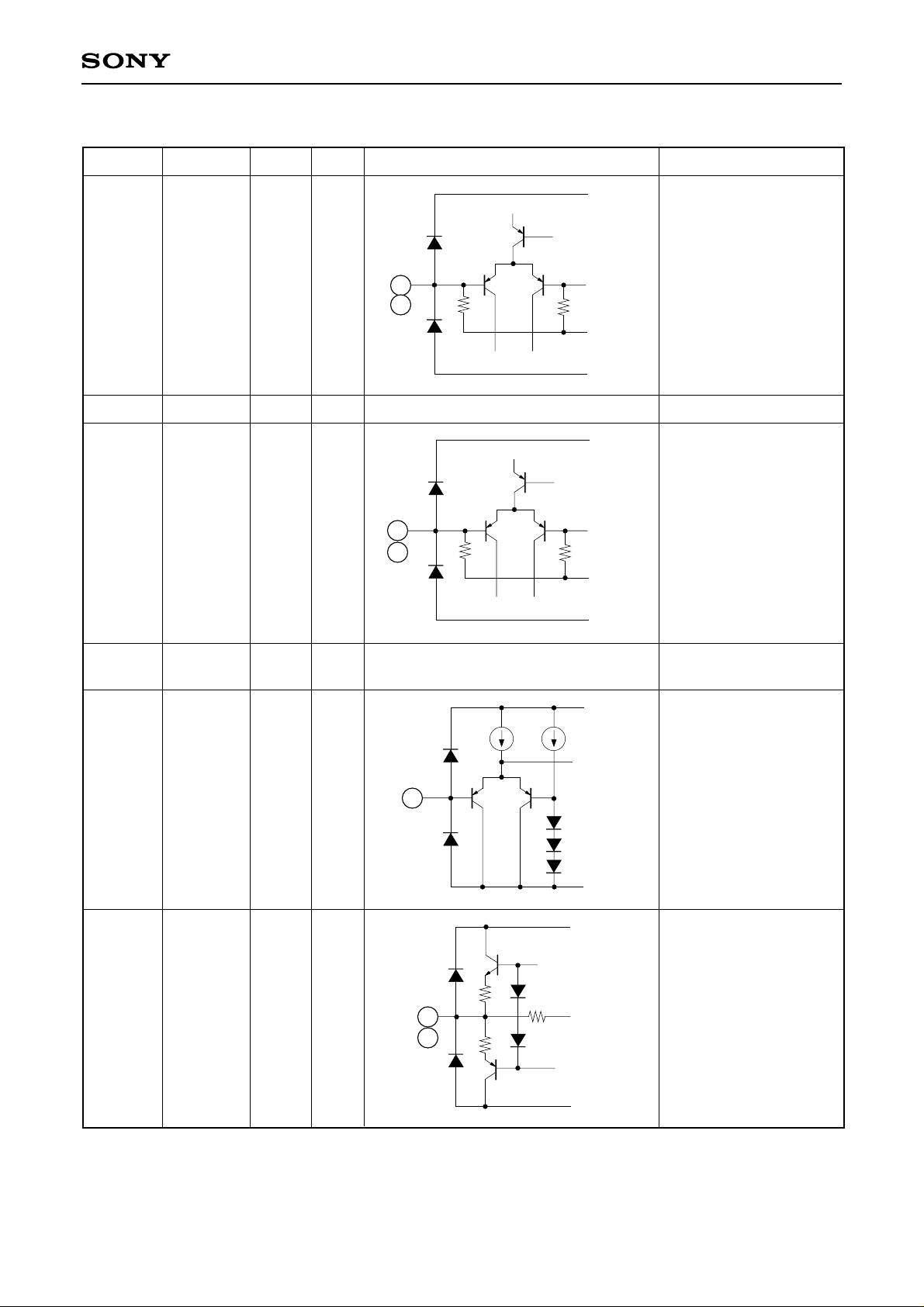
Pin Description (Ta = 25°C, VCC = 12V (Single supply), No signal)
No.
1, 16
2
3, 14
Symbol
REC IN
VCC
PB IN
Z (in)
40kΩ
—
40kΩ
VDC
6.0V
12.0V
6.0V
14
16
3
Equivalent Circuit
Vcc
1
40k
Vcc/2
GND
Description
Recording (Encode)
input
Power supply
Vcc
Playback (Decode) input
40k
Vcc/2
4
5
6, 11
VCC/2
ON/OFF
LINE OUT
1kΩ
—
—
6.0V
—
6.0V
GND
Single supply → VCC/2
Split supply → Ground
Vcc
50µ
150µ
Mode control pin for NR
ON/OFF
5
"H" → NR OFF
"L" → NR ON
GND
Vcc
150
11
6
150
Line (Decode) output
– 2 –
GND
Page 3
CXA1100/CXA1101/CXA1102/CXA1163
No.
7, 10
8, 9
Symbol
TC
REC OUT
Z (in)
—
—
VDC
0.3V
6.0V
Equivalent Circuit
7
10
8
9
8.2k
100k
300
300
4µ
8.2k
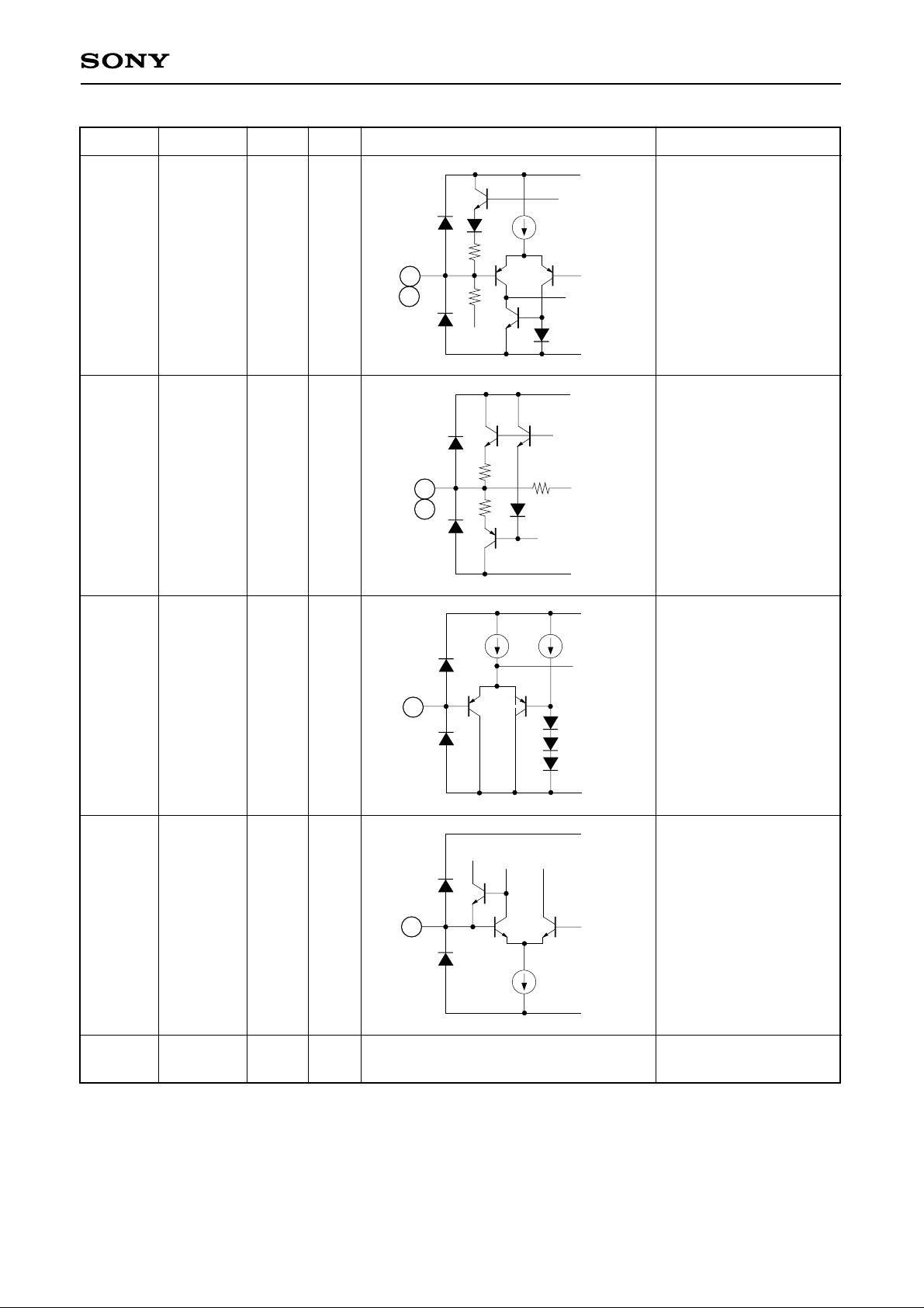
Description
Vcc
Time constant pin for
the level detector
GND
Vcc
Recording (Encode)
output
GND
12
13
15
REC/PB
IREF
GND
—
—
—
—
1.2V
0V
13
12
50µ 150µ
10µ
Vcc
GND
Vcc
1.2V
GND
Mode control pin for
REC/PB
(Encode/Decode)
"H" → B (Decode)
"L → EC (Encode)
Reference current input
pin for the active filters
Single supply → Ground
Split supply → VEE
– 3 –
Page 4
CXA1100/CXA1101/CXA1102/CXA1163
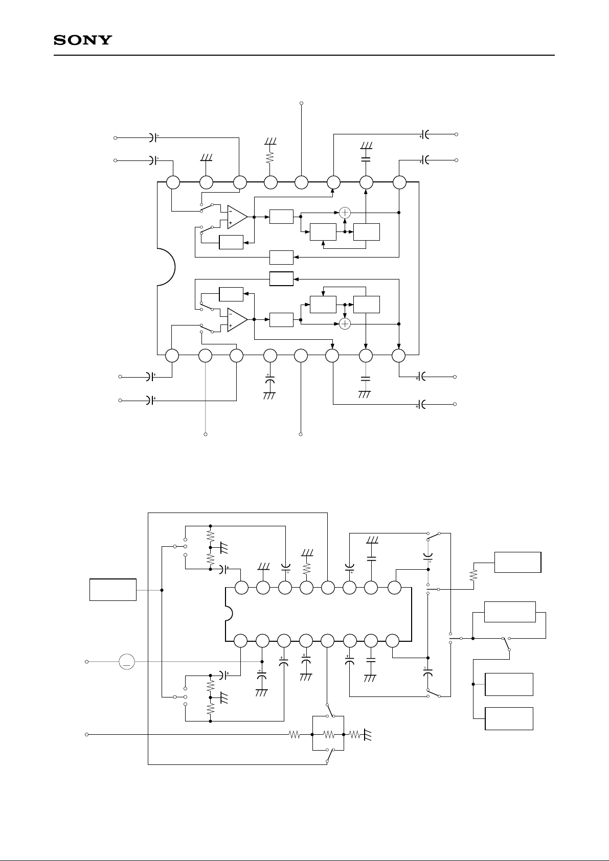
Block Diagram
PB IN
REC IN
REC IN
PB IN
C12
1µ
C11
1µ
C21
1µ
C22
1µ
16
REC/PB
C14
4.7µ
R1
43k
13
1415
ATT2
ATT2
ATT2
1
2
Vcc
3
ATT1
ATT3
ATT3
ATT3
ATT3
ATT1
4
C1
100µ
12
5
ON/OFF
11
SC DET
SC DET
SC DET
6
10
7
C13
0.68µ
C23
0.68µ
C15
9
8
4.7µ
C25
4.7µ
C24
4.7µ
LINE OUT
REC OUT
REC OUT
LINE OUT
ATT: Attenuator
SC : Side Chain
DET: Detector
Test Circuit
Vcc
+15V
Audio
SG
S5-1
P
R
DC Level
C16
4.7µ
1
9
2
S6-2
8
1
2
S6-1
C25
4.7µ
R
P
S5-2
R2
10k
CCIR/ARM
OFF
AC Level
Meter
Distortion
Analyzer
Meter
Filter
ON
S7
OFF
R11
5.1k
R21
5.1k
OFF
R12
5.1k
C11
1µ
R22
5.1k
C21
1µ
16
C12
1µ
R1
43k
13
4
100µ
C1
OFF
R4
2k
12
11
6
5
C24
4.7µ
S2
ON
510
P
R
S1
1415
1
2
3
C22
C2
1µ
100µ
R3
12k
R5
C14
4.7µ
C13
0.68µ
10
7
C23
0.68µ
P
S3
R
A
R
S4
P
– 4 –
Page 5
CXA1100/CXA1101/CXA1102/CXA1163
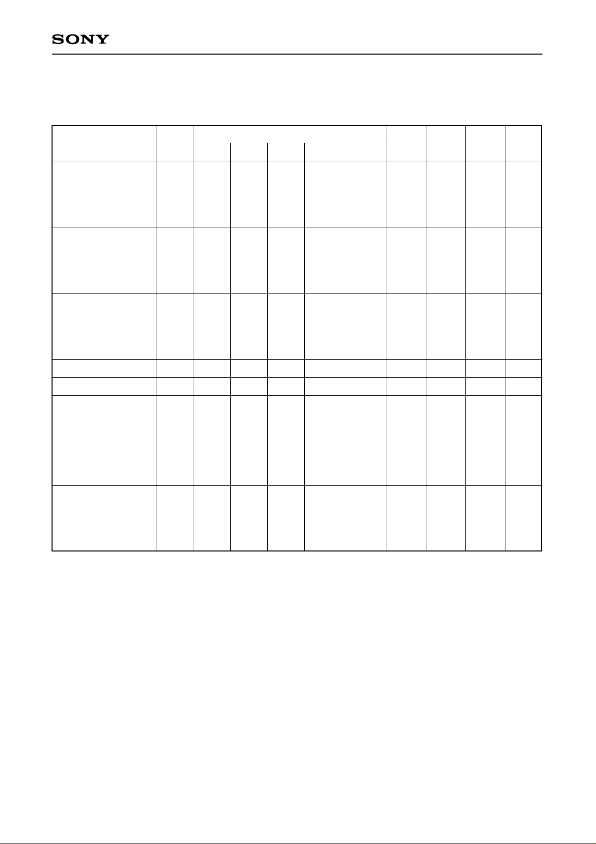
Electrical Characteristics Ta = 25°C, Dolby Level: –10dBm ( = 245mVrms) at REC OUT
VCC = 15V (CXA1100), VCC = 12V (CXA1101), VCC = 9V (CXA1102)
VCC = 6V (CXA1163)
Item Symbol
Test Condition
∗
Min. Typ. Max. Unit
R/P NR f (Hz) Other Conditions
Operating voltage
CXA1100
CXA1101
CXA1102
CXA1163
Supply current
CXA1100
CXA1101
CXA1102
CXA1163
LINE OUT level
CXA1100
CXA1101
CXA1102
CXA1163
REC IN level
PB IN level
Encode characteristics
(Boost)
(1)
(2)
(3)
(4)
(5)
Vopr
ICC
Vlout
Vrin
Vpin
B-R-1
B-R-2
B-R-3
B-R-4
B-R-5
—
—
R
R
R
P
R
R
R
R
R
OFF
OFF
OFF
OFF
ON
ON
ON
ON
ON
—
—
1k
1k
1k
500
2k
5k
10k
10k
Signal Handling
≥ 12dB
No signal
–25dB
–25dB
–25dB
–40dB
0dB
11.5
8.5
6.5
5.0
3.5
3.5
3.5
3.5
–1.0
–4.0
–7.0
–11.0
–32
–32
1.4
5.5
3.9
9.7
–1.1
—
—
—
—
5.6
5.5
5.3
5.1
0.0
–3.0
–6.0
–10.0
–30
–30
2.9
7.0
5.4
10.4
0.4
16.0
16.0
16.0
16.0
7.5
7.5
7.5
7.5
1.0
–2.0
–5.0
–9.0
–28
–28
4.4
8.5
6.9
11.9
1.9
V
V
V
V
mA
mA
mA
mA
dBm
dBm
dBm
dBm
dBm
dBm
dB
dB
dB
dB
dB
Signal handling
CXA1100
CXA1101
CXA1102
CXA1163
Vomax
R
OFF
1k
THD = 1%
13.5
14.0
14.0
13.0
15.3
15.9
15.9
15.0
—
—
—
—
dB
dB
dB
dB
0dBm = 0.775Vrms
– 5 –
Page 6
CXA1100/CXA1101/CXA1102/CXA1163
Item Symbol
Total harmonic
distortion
1) NR OFF
CXA1100
CXA1101
CXA1102
CXA1163
2) NR ON
CXA1100
CXA1101
CXA1102
CXA1163
Input impedance
REC IN
PB IN
Encode S/N ratio
Crosstalk
REC-PB
PB-REC
REC ch to ch
PB ch to ch
THD
(OFF)
THD
(ON)
Zrec
Zpb
SN
(CCIR)
CT-1
CT-2
CT-3
CT-4
Test Condition
∗
R/P NR f (Hz) Other Conditions
R
R
—
—
R
P
R
R
P
OFF
ON
—
—
ON
OFF
OFF
OFF
OFF
1k
1k
1k
1k
—
1k
1k
1k
1k
+10dB
+10dB
Rg = 5kΩ
(CCIR/ARM)
0dB
0dB
0dB
0dB
Min. Typ. Max. Unit
—
—
—
—
—
—
—
—
28
28
65
—
—
—
—
0.03
0.04
0.05
0.06
0.03
0.04
0.06
0.09
40
40
69
–82
–81
–70
–70
0.2
0.2
0.2
0.2
0.3
0.3
0.3
0.3
57
57
—
–65
–60
–60
–60
%
%
%
%
%
%
%
%
kΩ
kΩ
dB
dB
dB
dB
dB
REC OUT
Offset voltage
Voff
R
ON
—
–40
0
40
(NR ON — OFF)
Control voltage
"H" Level
"L" Level
∗
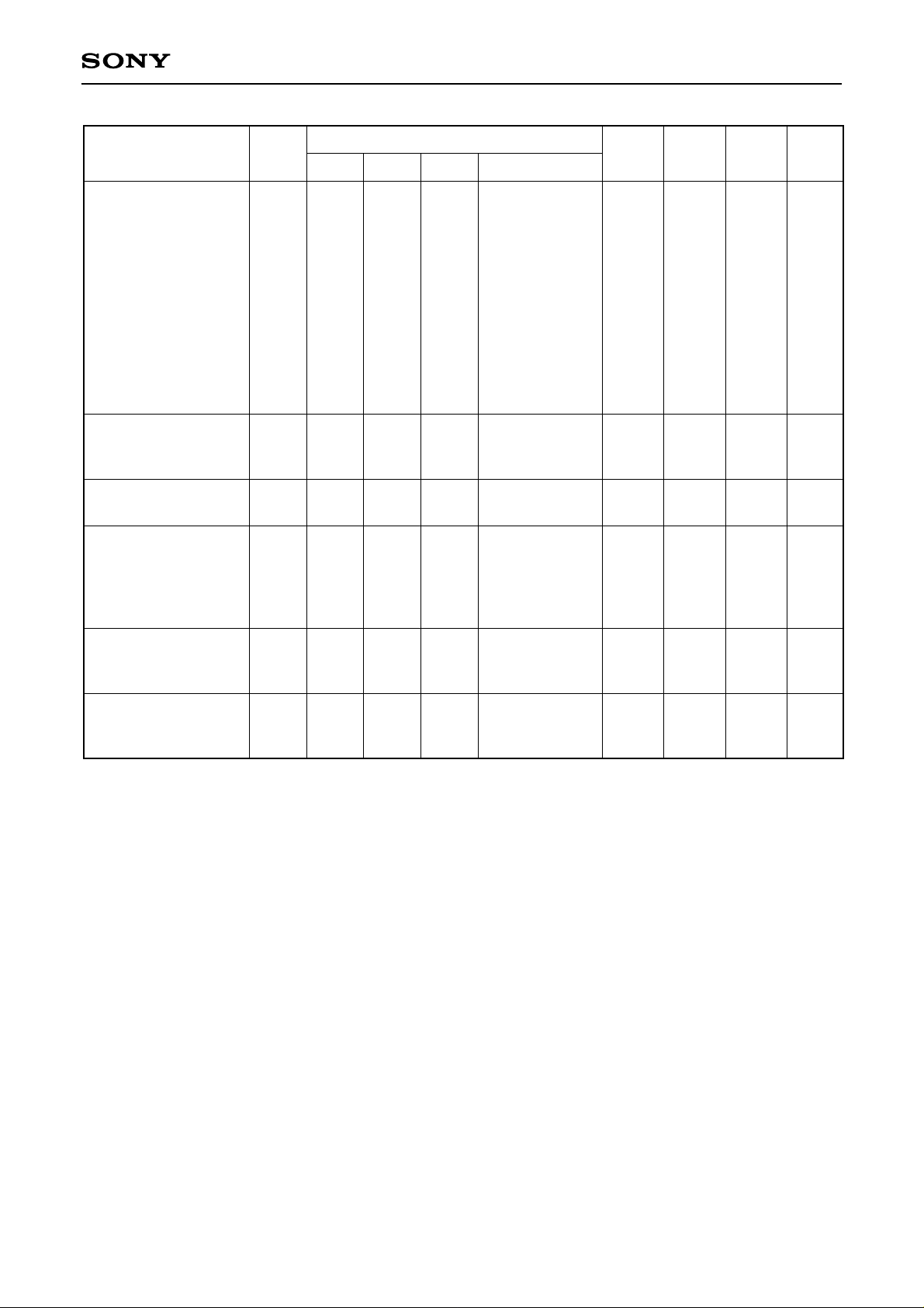
0dB means the level which provides the Dolby level at the recording output in the noise reduction off mode.
VC-H
VC-L
—
—
—
—
—
—
2.5
0
—
—
VCC
0.5
mV
V
V
– 6 –
Page 7
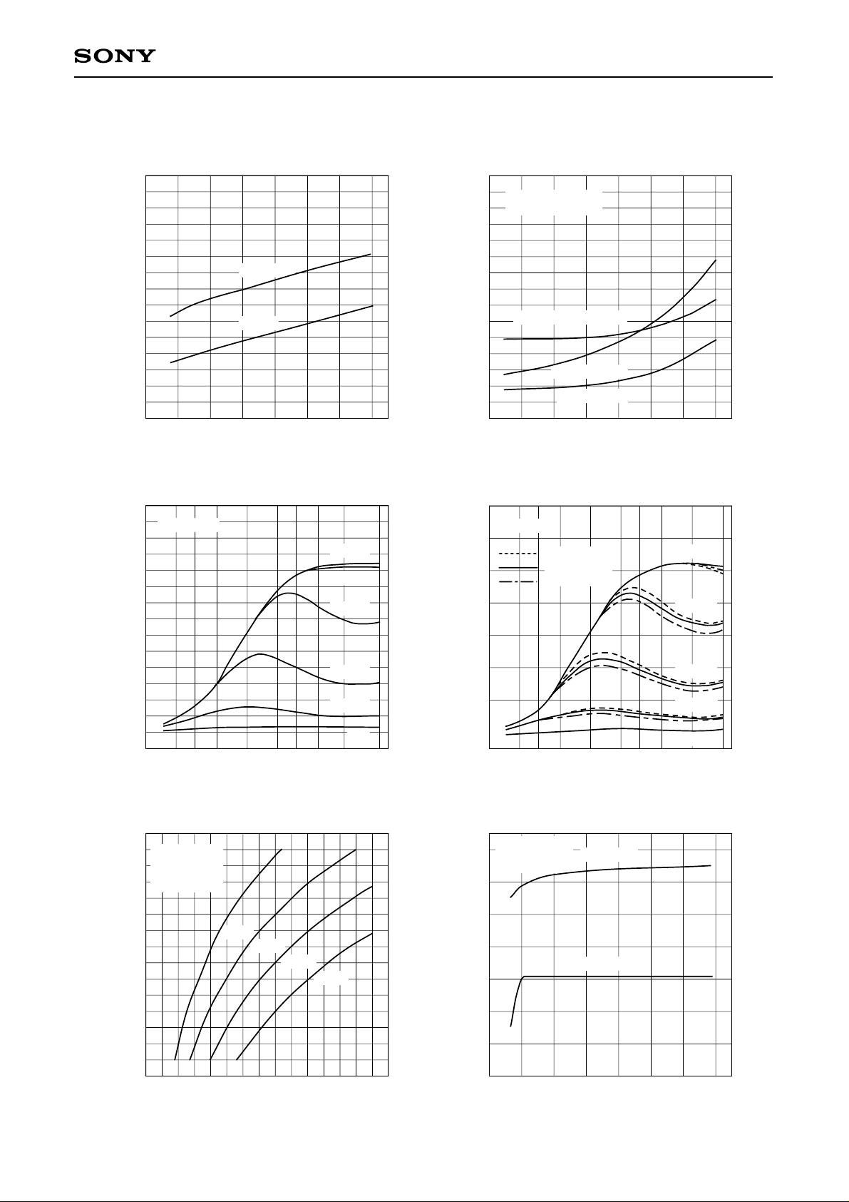
Example of Representative Characteristics
CXA1100/CXA1101/CXA1102/CXA1163
Quiescent Current vs. Supply Voltage
6.0
5.6
5.2
4.8
4.4
Icc — Quiescent current [mA]
4.0
3.6
4 6 8 10121416
NR OFF
NR ON
Vcc — Supply voltage [V]
Encode Characteristics
VCC = 12V
12
10
8
–50dB
–40dB
–30dB
Supply Current vs. Input Voltage
Encode Mode
6.8
0dB = Dolby Level
6.4
6.0
5.6
5.2
Icc — Supply current [mA]
4.8
4.4
NR OFF 1kHz, 10kHz
NR ON 10kHz
NR ON 1kHz
–12 –8 –4 0 4 8 12
Input level [dB]
Temperature Characteristics
VCC = 12V
12
Ta = –25°C
10
8
Ta = 25°C
Ta = 75°C
(CXA1101)
–40dB
–30dB
6
4
Encode boost [dB]
2
0
200 500 1k 2k 5k 10k 20k
Encode Mode
NR OFF
20
f = 1kHz
THD = 1%
18
16
14
12
Signal handling [dB]
10
8
4 6 8 10121416
Frequency [Hz]
Signal Handling
A1163
A1102
A1101
A1100
Vcc — Supply voltage [V]
–20dB
–10dB
0dB
6
4
Encode boost [dB]
2
0
200 500 1k 2k 5k 10k 20k
Frequency [Hz]
Load Characteristics
(CXA1101)
Encode Mode
14
VCC = 12V
THD = 1%
12
10
8
6
4
Maximum output level [dBm]
2
0
1234567
L — Load resistance [kΩ]
R
–20dB
–10dB
0dB
LINE OUT
REC OUT
– 7 –
Page 8

CXA1100/CXA1101/CXA1102/CXA1163
NR o f f Tot al Ha rrm onic Dis t o rt io n-1
(CX A 1101)
1.0
Encode Mode
VCC = 12V
0.5
0dB = Dolby Level
0.2
0.1
0.05
To tal Harmon ic Disttortio n [% ]
0.02
0.01
–8
Output Level [dB]
f = 100Hz
f = 1kHz
f = 10kHz
16–4 0 4 8 12
To tal Harmon ic Disttortio n [% ]
NR o f f Tot al Ha rrm onic Dis t o rt io n-2
(CX A 1100)
1.0
Encode Mode
0dB = Dolby Level
0.5
f = 1kHz
NR o nTot al Ha rrm onic Dis t o rt io n-1
(CX A 1101)
1.0
Encode Mode
VCC = 12V
0.5
0dB = Dolby Level
0.2
0.1
0.05
0.02
0.01
–8
Output Level [dB]
NR o nTot al Ha rrm onic Dis t o rt io n-2
(CX A 1100)
1.0
Encode Mode
0dB = Dolby Level
0.5
f = 1kHz
f = 100Hz
f = 1kHz
f = 10kHz
16–4 0 4 8 12
0.2
0.1
0.05
0.02
To tal Harmon ic Disttortio n [% ]
0.01
–8
Output Level [dB]
VCC = 15V
VCC = 11.5V
16–4 0 4 8 12
NR o f f Tot al Ha rrm onic Dis t o rt io n-3
(CX A 1101)
1.0
Encode Mode
0dB = Dolby Level
0.5
f = 1kHz
0.2
0.1
0.05
0.2
0.1
0.05
0.02
To tal Harmon ic Disttortio n [% ]
0.01
–8
Output Level [dB]
VCC = 15V
VCC = 11.5V
16–4 0 4 8 12
NR o nTot al Ha rrm onic Dis t o rt io n-3
(CX A 1101)
1.0
Encode Mode
0dB = Dolby Level
0.5
f = 1kHz
0.2
0.1
0.05
To tal Harmon ic Disttortio n [% ]
0.02
0.01
–8
Output Level [dB] Output Level [dB]
VCC = 15V
VCC = 12V
VCC = 8.5V
16–4 0 4 8 12
To tal Harmon ic Disttortio n [% ]
0.02
0.01
–8
VCC = 15V
VCC = 12V
VCC = 8.5V
16–4 0 4 8 12
– 8 –
Page 9
CXA1100/CXA1101/CXA1102/CXA1163
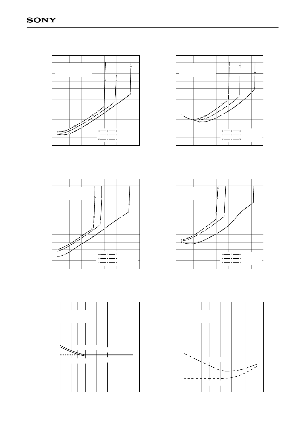
NR o f f Tot al Ha rm onic Dis t o rt io n-4
(CX A 1102)
1.0
Encode Mode
0dB = Dolby Level
0.5
f = 1kHz
0.2
0.1
0.05
To tal Harmon ic Disto rt ion [%]
0.02
0.01
Output Level [dB]
VCC = 15V
VCC = 9 V
VCC = 6.5V
20
16–4 0 4 8 12
To tal Harmon ic Disto rt ion [%]
NR o f f Tot al Ha rm onic Dis t o rt io n-5
(CX A 1163)
1.0
Encode Mode
0dB = Dolby Level
0.5
f = 1kHz
NR o n Tot al Ha rm onic Dis t o rt io n-4
(CX A 1102)
1.0
Encode Mode
0dB = Dolby Level
0.5
f = 1kHz
0.2
0.1
0.05
0.02
0.01
Output Level [dB]
NR o n Tot al Ha rm onic Dis t o rt io n-5
(CX A 1163)
1.0
Encode Mode
0dB = Dolby Level
0.5
f = 1kHz
VCC = 15V
VCC = 9 V
VCC = 6.5V
20
16–4 0 4 8 12
0.2
0.1
0.05
To tal Harmon ic Disto rt ion [%]
0.02
0.01
VCC = 15V
VCC = 6 V
VCC = 5 V
200 4 8 12 16
24
Channel t o C hannel Crosstalk
(CXA 1101)
–30
VCC = 12V/±6V
NR off
–40
C1 (Pin4) = 100µF
–50
–60
–70
Crosstalk [dB]
–80
Single Supply
Split Supply
Encode
Decode
0.2
0.1
0.05
To tal Harmon ic Disto rt ion [%]
0.02
0.01
Output Level [dB]Output Level [dB]
VCC = 15V
VCC = 6 V
VCC = 5 V
200481216
24
REC t o PB and PB t o REC C rosstalk
(CXA 1101)
–30
VCC = 12V/±6V
NR off
–40
C1 (Pin4) = 100µF
–50
–60
–70
Crosstalk [dB]
–80
Single Supply
–90
Frequency [Hz]
–90
10k
5k2k1k500200100
Split Supply
Frequency [Hz]
10k
5k2k1k500200100
– 9 –
Page 10

CXA1100/CXA1101/CXA1102/CXA1163
Ripple Rejection Ratio-1
Encode Mode
–10
VCC = 12V Single Supply
–20
–30
–40
–50
Ripple rejection ratio [dB]
–60
–70
C1 (Pin4) = 100µF
Ripple Rejection Ratio-3
VCC Rejection
–10
VCC, VEE = ±6V
–20
–30
–40
–50
Ripple rejection ratio [dB]
–60
(CXA1101)
Frequency [Hz]
(CXA1101)
NR on
C1 (Pin4)
= 470µF
NR off
NR off
NR on
5k2k1k500200100
Encode
Decode
10k
Ripple Rejection Ratio-2
Decode Mode
VCC = 12V Single Supply
–10
–20
–30
–40
–50
Ripple rejection ratio [dB]
–60
–70
C1 (Pin4) = 100µF
Ripple Rejection Ratio-4
0
–10
–20
–30
–40
Ripple rejection ratio [dB]
–50
VEE Rejection
VCC, VEE = ±6V
(CXA1101)
C1 (Pin4) = 470µF
Frequency [Hz]
(CXA1101)
NR on
NR off
5k2k1k500200100
Encode
Decode
NR on
NR off
10k
–70
Frequency [Hz]
10k
5k2k1k500200100
–60
Frequency [Hz]
10k
5k2k1k500200100
Notes on Applications
1) Power supply
The CXA1100 Series is basically designed to operate on single ended supply. The split supply operation is
also possible, however, VEE (negative) supply should provide low noise and ripple characteristics. The
ripple rejection ratio of these devices is generally good for Vcc supply (single ended supply and split
supply), however, that for VEE supply is not so good in the NR on mode because the integrated capacitors
for the side chain filter are connected to pin 15 (VEE on split supply).
– 10 –
Page 11
CXA1100/CXA1101/CXA1102/CXA1163
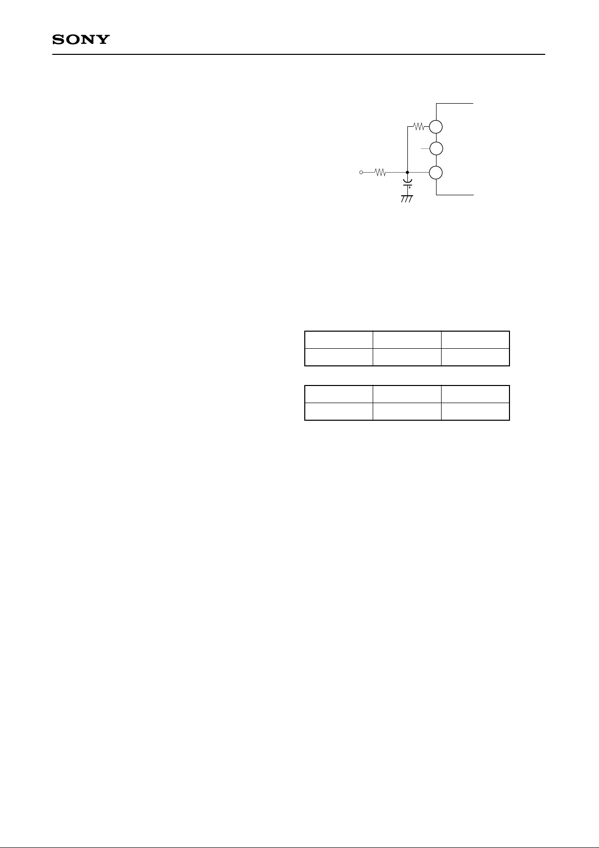
When the ripple or noise component of VEE supply is not negligible small, the CR filter shown in Fig. a-1 will
be usefull.
The operation voltage range are
CXA1100 11.5 to 16V (±5.75 to ±8V)
CXA1101 8.5 to 16V (±4.25 to ±8V)
CXA1102 6.5 to 16V (±3.25 to ±8V)
CXA1163 5.0 to 16V (±2.5 to ±8V)
V
EE
100 to 470µF
47
R1
43k
13
14
15
CXA1100
Series
Fig. a-1.
The devices will satisfy the signal handling of 12dB specified by Dolby Laboratories on above voltage range.
2) Operation mode control
The CXA1100 series provide fully electronic switching circuits. The functions are controlled by DC voltages
of the two control pins of REC/PB (pin 12) and ON/OFF (pin 5). The switching truth tables are shown in Fig. a-2.
VH and VL are defined as
(a) Single ended supply operation
REC/PB
Function
VH
PB (Decode)VLREC (Encode)
VCC ≥ VH ≥ 2.5V
0.5V ≥ VL ≥ 0V
ON/OFF
VH
VL
(b) Split supply operation
VCC ≥ VH ≥ VEE + 2.5V
Function
NR off
NR on
VEE + 0.5V ≥ VL ≥ VEE Fig. a-2.
It is desirable to provide CR time constant circuits at the mode control pins with time constant from
100msec to 1sec, which will reduce switching clicks effectively.
3) Reference levels
Characteristics and specifications of the Dolby noise reduction processor are defined as the levels and
measured with reference to the Dolby level. This particular level in these devices is –10dBm (245mVrms),
and is measured at the recording output (REC OUT) in the NR off mode.
The reference levels of the recording input (REC IN), play back input (PB IN) and line output (LINE OUT)
are defined the levels which provide the Dolby level at the recording output in the NR off mode.
The CXA1100 series has a common silicon die, and has different internal connection. The series provides
four different line output levels for various applications. Other reference levels, recording input level,
playback input level and recording output level (= Dolby level) are identical in all devices.
The reference levels are as follows
Recording output level (= Dolby level) –10dBm (245mVrms)
Recording input level –30dBm (24.5mVrms)
Play back input level –30dBm (24.5mVrms)
Line output level CXA1100 0dBm (775mVrms)
CXA1101 –3dBm (548mVrms)
CXA1102 –6dBm (388mVrms)
CXA1163 –10dBm (245mVrms)
– 11 –
Page 12
CXA1100/CXA1101/CXA1102/CXA1163
4) MPX filter termination and C1 for Vcc/2 (Pin 4)
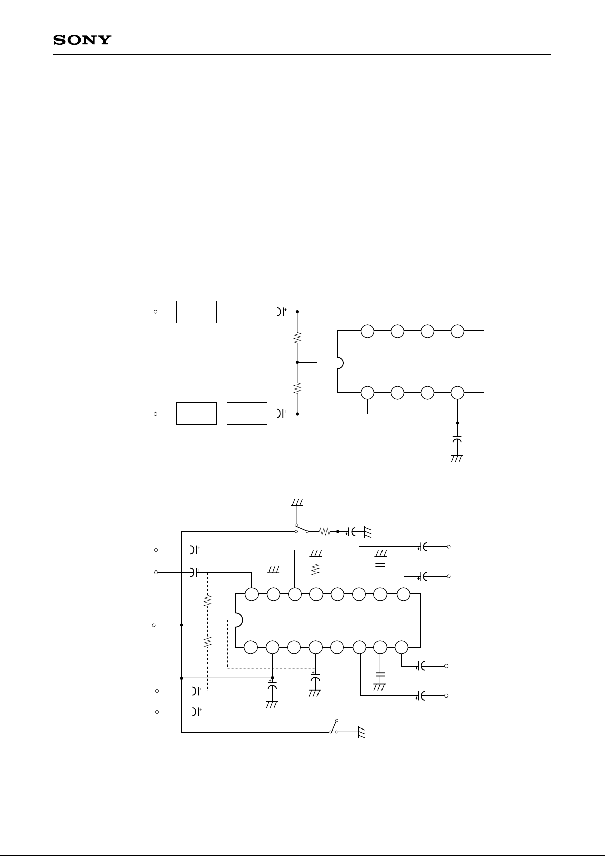
The MPX (multiplex) filter termination method shown in Fig. a-3 allows saving the coupling capacitors
between the buffer amplifiers and MPX filters. However, the channel to channel separation and REC to PB
crosstalk of low frequency signals will be degraded by the termination resistor RT. For example, 5kΩ of R1
will degrade the channel to channel separation to 50dB. Better separation can be obtained by increasing
the capacitance of C1 (Pin 4) to 220µF or 470µF.
The allowable minimum value of C1 is 47µF, and 100µF is the standard recommended value. Larger values
of C1 are generally desirable in order to improve the crosstalk and ripple rejection ratio.
5) Application for dubbing cassette decks
The CXA1100 series generates non decoded signal at the recoding output in the decode mode, and can
simplify the structure of dubbing decks. See the SONY' Dolby B/C type IC (CX20187/CXA1097Q or
CX20188/CXA1098Q) data sheet in detail.
C11
Line
Input
MPX
Buffer
Filter
MPX
MPX
Filter
Filter
4.7µ
RT
16
13
1415
Line
Input
MPX
Buffer
Filter
MPX
MPX
Filter
Filter
Switchable Processor with Single Supply
PB IN
(–30dBm)
REC IN
(–30dBm)
V
REC IN
(–30dBm)
PB IN
(–30dBm)
CC
C11
1µ
∗
C12
1µ
C21
1µ
C22
1µ
∗
R
T
∗
RT
16
CXA1100 Series
RT
C21
4.7µ
1
2
4
3
C1
470µ
Fig. a-3.
C3
R2
10k
R1
(12
%)
43k
∗
C1
100µ
OFF
12
5
NR
ON/OFF
ON
10µ
11
C14
4.7µ
LINE OUT
C13 (10%)
0.68µ
9
10
6
8
7
C23 (10%)
0.68µ
C24
4.7µ
C15
4.7µ
C25
4.7µ
REC OUT
REC OUT
(–10dBm)
LINE OUT
REC/PB
REC
PB
13
1415
1
2
C2
100µ
4
3
Note 1) Resistor and capacitor tolerances are ±10% and ±20% respectively unless otherwise specified.
Note 2) When resistors RT are connected to Pin 4 for the MPX filter termination, increase the capacitances of
C1 and C11 (C21) to 470µF and 4.7µF respectively.
– 12 –
Page 13
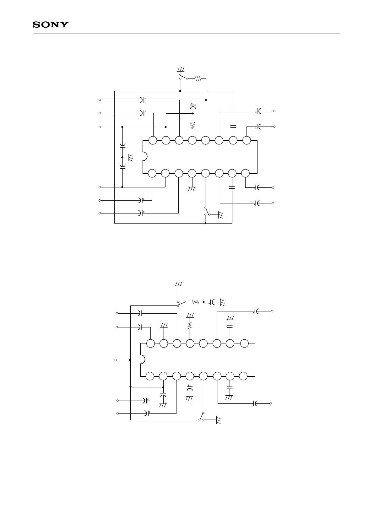
Switchable Processor with Split Supply
PB IN
(–30dBm)
REC IN
(–30dBm)
EE
V
CC
V
REC IN
(–30dBm)
PB IN
(–30dBm)
C12
1µ
C11
1µ
C1
100µ
C2
100µ
C21
1µ
C22
1µ
16
1
2
PB
REC
1415
3
NR
ON/OFF
REC/PB
R2
10k
C3
10µ
R1
(12
%)
43k
13
4
ON
12
5
OFF
11
6
C13 (10%)
0.68µ
9
10
8
7
C23 (10%)
0.68µ
CXA1100/CXA1101/CXA1102/CXA1163
C14
4.7µ
C15
4.7µ
C25
4.7µ
C24
4.7µ
LINE OUT
REC OUT
(–10dBm)
REC OUT
(–10dBm)
LINE OUT
Note 1) Resistor and capacitor tolerances are ±10% and ±20% respectively unless otherwise specified.
Playback Processor with AUX input
TAPE/AUX
TAPE IN
(–30dBm)
AUX IN
(–30dBm)
CC
V
AUX IN
(–30dBm)
TAPE IN
(–30dBm)
∗
C21
C22
1µ
1µ
C11
1µ
∗
C12
1µ
16
AUX
TAPE
1
2
C2
100µ
∗
∗
R2
∗
13
1415
3
10k
R1
(2%)
43k
4
C1
100µ
OFF
C3
10µ
12
5
NR
ON/OFF
ON
11
10
6
7
C13 (10%)
0.68µ
C14
4.7µ
LINE OUT
C13 (10%)
0.68µ
9
8
LINE OUT
C24
4.7µ
Note 1) Resistor and capacitor tolerances are ±10% and ±20% respectively unless otherwise specified.
Note 2) When AUX inputs are not necessary, reject R2, C3, C11, C21 and TAPE/AUX switch, and connect Pin 12
to Vcc.
– 13 –
Page 14
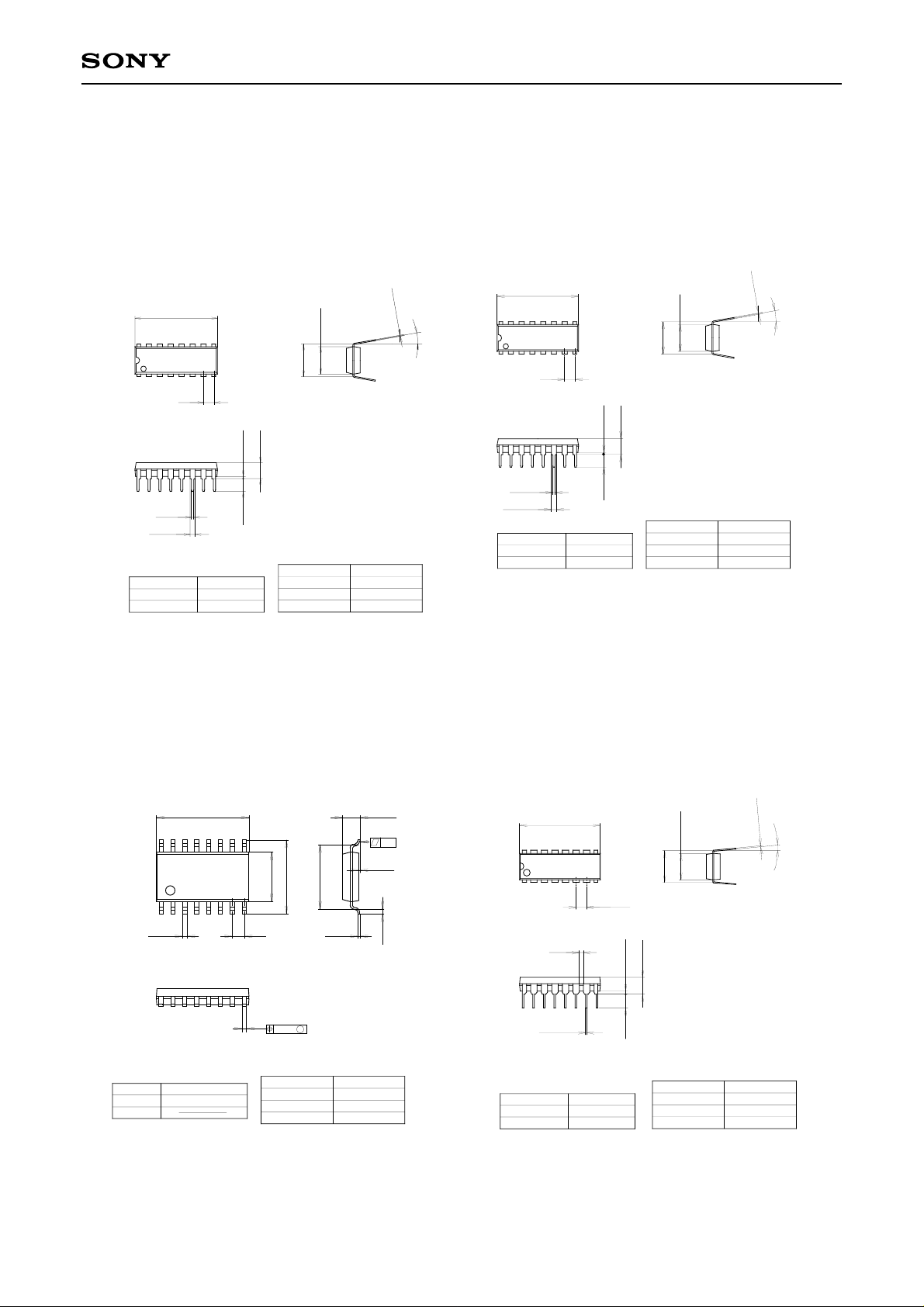
Package Outline Unit: mm
CXA1101P, CXA1101P
CXA1102P, CXA1163P
CXA1100/CXA1101/CXA1102/CXA1163
16PIN DIP (PLASTIC) 300mil
+ 0.4
19.2 – 0.1
16
18
0.5 ± 0.1
1.2 ± 0.15
SONY CODE
EIAJ CODE
JEDEC CODE
2.54
9
0.5 MIN
3.0 MIN
DIP-16P-01
∗DIP016-P-0300-A
Similar to MO-001-AE
+ 0.4
3.7 – 0.1
PACKAGE STRUCTURE
+ 0.3
6.4 – 0.1
7.62
PACKAGE MATERIAL
LEAD TREATMENT
LEAD MATERIAL
PACKAGE WEIGHT
+ 0.1
EPOXY RESIN
SOLDER PLATING
COPPER
1.0 g
0.25 – 0.05
0° to 15°
1
0.46 ± 0.1
1.53 ± 0.15
SONY CODE
EIAJ CODE
JEDEC CODE
+ 0.4
19.1 – 0.1
2.54
16PIN DIP (PLASTIC) 300mil
916
7.62
8
+ 0.4
0.5 MIN
3.7 – 0.1
3.0 MIN
DIP-16P-03
∗DIP016-P-0300-B
Similar to MO-001-AE
PACKAGE STRUCTURE
PACKAGE MATERIAL
LEAD TREATMENT
LEAD MATERIAL
PACKAGE WEIGHT
+ 0.3
6.4 – 0.1
+ 0.1
0.25 – 0.05
0° to 15°
EPOXY RESIN
SOLDER PLATING
COPPER / 42 ALLOY
1.0g
CXA1101M, CXA1102M
CXA1163M
16PIN SOP (PLASTIC) 300mil
+ 0.4
9.9 – 0.1
16
18
0.45 ± 0.1
SONY CODE
SOP-16P-L01
∗SOP016-P-0300-A
EIAJ CODE
JEDEC CODE
9
+ 0.3
5.3 – 0.1
7.9 ± 0.4
1.27
M
± 0.12
PACKAGE STRUCTURE
PACKAGE MATERIAL
LEAD TREATMENT
LEAD MATERIAL
PACKAGE WEIGHT
6.9
+ 0.1
0.2 – 0.05
EPOXY RESIN
SOLDER PLATING
COPPER ALLOY
0.2g
+ 0.4
1.85 – 0.15
0.15
+ 0.2
0.1 – 0.05
0.5 ± 0.2
CXA1100P, CXA1101P
CXA1102P
16PIN DIP (PLASTIC) 300mil
19.35 ± 0.5
916
1
SONY CODE
EIAJ CODE
JEDEC CODE
0.457 ± 0.076
1.016
8
2.54 ± 0.254
DIP-16P-191
DIP016-P-0300-AU
MS-001-AA
0.508 MIN
3.1 MIN
6.35 ± 0.127
7.62
5.08 MAX
PACKAGE STRUCTURE
PACKAGE MATERIAL
LEAD TREATMENT
LEAD MATERIAL
PACKAGE WEIGHT
+ 0.1
0.28 – 0.06
EPOXY RESIN
SOLDER PLATING
COPPER
1.0g
0° to 10°
– 14 –
Page 15

CXA1100P, CXA1101P/M, CXA1102P/M, CXA1163P/M
16PIN SOP (PLASTIC) 300mil
CXA1100/CXA1101/CXA1102/CXA1163
+ 0.3
∗10.2 – 0.1
16
1.27 ± 0.1
SONY CODE
EIAJ CODE
JEDEC CODE
1
0.15
SOP-16P-L122
SOP016-P-0300-BX
0.71 ± 0.1
NOTE: Dimension “∗” does not include mold protrusion.
0.4 ± 0.1
9
8
0.13
+ 0.3
7.8 ± 0.1
∗5.3 – 0.1
M
0.15 ± 0.05
PACKAGE STRUCTURE
PACKAGE MATERIAL
LEAD TREATMENT
LEAD MATERIAL
PACKAGE WEIGHT
2.0 MAX
0.05 MIN
1.8
0.75 ± 0.2
4° to 8°
EPOXY RESIN
SOLDER PLATING
COPPER
0.21g
– 15 –
 Loading...