

Page 1
CORPORATION
IN
IN
IN
IN
S
D
3
4
1
2
S
D
S
D
S
D
1
1
2
2
3
3
4
4
IN
IN
IN
IN
S
D
3
4
1
2
S
D
S
D
S
D
1
1
2
2
3
3
4
4
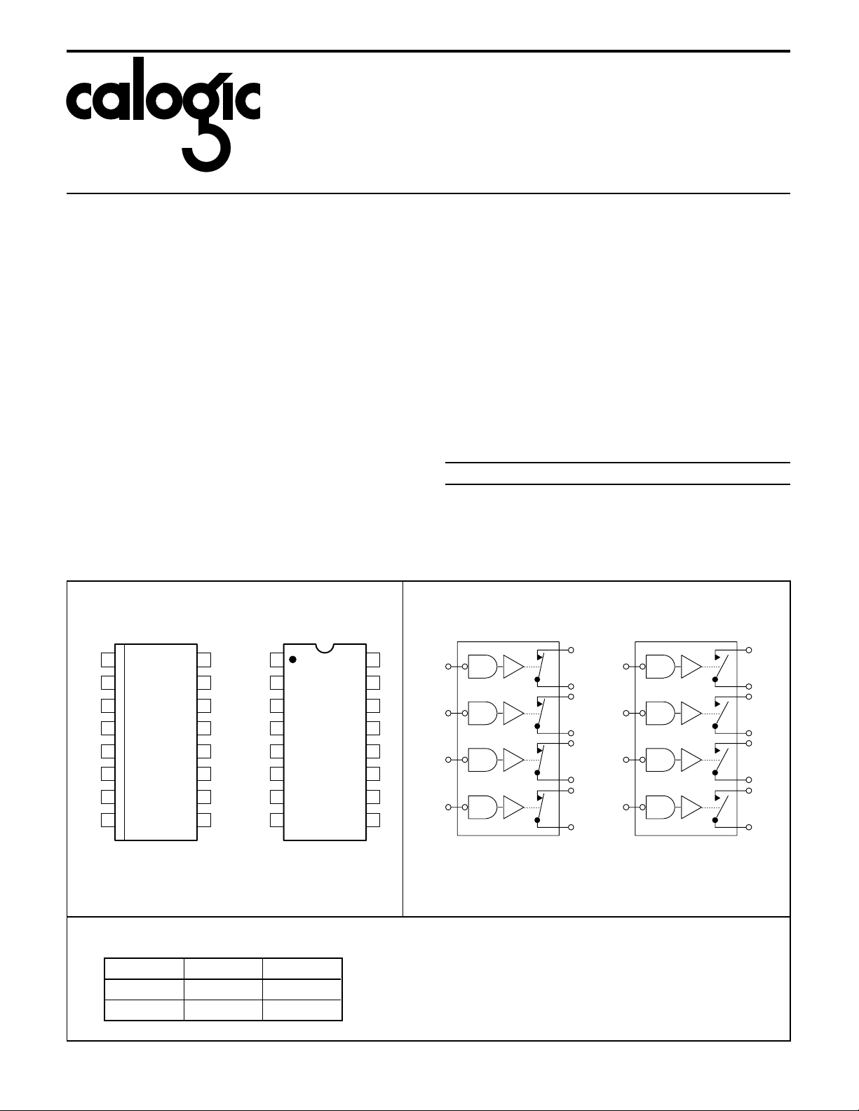
Four SPST Switches per Package.
Switches shown in Logic '1' Input Position.
CWB308 CWB309
CMOS/DMOS
Quad Monolithic SPST
Wide Band Analog Switches
CWB308 / CWB30 9
FEATURES
Low Inserti on Lo s s . . . . . . . . . . . . . 0.9 x DC @ 100MHz
••
Low Channel-to-Chan nel Crosstalk. . . . . . . . . . . . -80dB
••
High OFF Isolation . . . . . . . . . . . . . . . . . 68dB @ 10MHz
••
Fast Switching . . . . . . . . . . . . . . . . . . . . . . . . . . . <140ns
••
Low ON Resistance . . . . . . . . . . . . . . . . . . . . . . 40Ω (typ)
••
APPLICATIONS
High Speed M ul tip le xi ng
••
RF & Video Sw itc h es
••
Sample and Hold Sw itch es
••
Track and Hol d Switc hes
••
Comp u te r Pe r ip he r al s
••
PIN CONFIGURATION FUNCTIONAL BLOCK DIAGRAMS
1
IN1
2
D1
3
S1
4
V-
5
GND
6
S4
7
D4
IN4
8
CWB
LOGIC TABLE
CWB308CY
CWB309CY
Logic CWB308 CWB309
0 OFF ON
1 ON OFF
DESCRIPTION
The Calogic CWB308 and CWB309 feature fast switching
(<140ns) and low ON resistance (<40Ω) for excellent
performance in applications in communications, computer
peripherals and instrument controls. This series combines
low power CMOS input logic and level translation circ uitr y with
high speed, low capacitance DMOS sw itches in a monolithic
structure. The CWB308 and CWB309 have CMOS
compatible inputs and also have a standard pin configuration
for second sourcing.
ORDERING INFORMATION
Part Package Temperature Range
o
CWB308CP Plastic 16-Pin Dip 0 to +85
CWB308CY Plastic SO-16 Surface Mount 0 to +85
XCWB308 Sorted Chips in Carriers 0 to +85
CWB309CP Plastic 16-Pin Dip 0 to +85
CWB309CY Plastic SO-16 Surface Mount 0 to +85
XCWB309 Sorted Chips in Carriers 0 to +85
16-PIN DIPSO-16
16
IN2
15
D2
14
S2
13
V+
12
N/C
11
S3
10
D3
9
IN3
IN1
D1
S1
GND
S4
D4
IN4
1
2
3
4
V-
5
6
7
8
TOP VIEWTOP VIEW
CWB308CP
CWB309CP
IN2
16
D2
15
S2
14
V+
13
N/C
12
S3
11
D3
10
IN3
9
All devi ces con tain diod es t o pro tect inputs against d amage d ue
to high static vo ltag e s or ele ctri c fie lds; ho wever, it is advised that
precautions be taken not to exceed the maximum recommended
input voltages. All unused inputs must be connected to an
appropriate logic level (either V
or GND).
cc
C
o
C
o
C
o
C
o
C
o
C
Page 2
CWB308 / CWB3 09
CORPORATION
ABSOLUTE MAXIMUM RATINGS
V- Negative Supply Voltage . . . . . . . . . . . . . . . . . . . . -20 V
V+ Positive Supply Volt age. . . . . . . . . . . . . . . . . . . . . +20V
Control Input Vo ltag e Range . . . . . . . . . . . . . . V+ +0.3V
V
IN
V- -0.3V
Continuous Current, any Pin excep t S or D. . . . . . 20mA
I
L
I
Continuou s Curre nt, S or D . . . . . . . . . . . . . . . . . . 30mA
S
Peak Pulsed Current, S or D, 80µsec, 1%,
I
S
RECOMMENDED OPERAT ING CONDITION S
V- Negative Supply Voltage . . . . . . . . . . . . . . . -8.0 to -15V
V+ Positive Supply V olt age. . . . . . . . . . . . . . . +8.0 to +15V
Control Input Vo ltage Range . . . . . . . . . . . . . . 0 to +5V
V
IN
Analog Switch V olt age Ran ge. . . . . . . . . . . -10 to +10V
V
S
Operating Temperature . . . . . . . . . . . . . . . . 0 to +85oC
T
OP
Duty Cycle . . . . . . . . . . . . . . . . . . . . . . . . . . . . . 180mA
Junction Tempe ra ture Range. . . . . . . . . . -55 to +125oC
T
J
Storage Temper ature Ran ge. . . . . . . . . . -55 to +125oC
T
S
P
Power Dissipation . . . . . . . . . . . . . . . . . . . . . . . 500mW
D
ELECTRICAL CHARACTERISTICS (V- = -15V, V+ = +15V unle ss otherwise n ot ed, T
SYMBOL PARAMETER MIN TYP MAX UNITS TEST CONDITIONS
STATIC
V
ANALOG
r
DS(ON)
V
IH
V
IL
I
IN
I
D(OFF)
I
S(OFF)
I- Negative Supply Quiescent Current -0.1 -0.5
I+ Positive Supply Quiescent Current 0.1 0 .5
DYNAMIC
t
ON
t
OFF
O
IRR
C
CRR
C
d
C
s
Analog Signal Range -10 +10 V
40 80
Switch ON Resistance
45 80 V
100 160 V
High Level Input Voltage 4.5 3.4
Low Level Input Voltage 1.0
Logic Input Leakage Current
Switch OFF Leakage Current
0.01 0.1
0.02 0.1 V
0.2 5.0
0.4 5.0 VS = +10V, VD = -10V
Switch Turn-ON Time 140 250
Switch Turn-OFF Time 80 220
Off Isolation Rejection Ratio 60 62
Cross-Coupling Rejection Ratio 80 f = 10MHz, RL = 50Ω
Drain-Node Capacitance 0.3
Source-Node Cap acita nce 3.0
= +25oC)
A
ohms
V
µA
nA
µA
nSec
dB
pF
V
= -10V
S
= +2.0V
S
= +10V
S
V
= +5.0V
IN
= +15V
IN
V
= +10V, VS = -10V
D
V
= 1.0V CWB308
IN
V
= 5.0V CWB309
IN
f = 10MHz, RL = 50Ω
VIN = 1.0V CGWB308
V
= 5.0V CWB309
IN
V
= VS = 0, f = 1MHz
D
CWB309
V
= 5.0V
IN
CWB308
V
= 1.0V
IN
Page 3
CORPORATION
ELECTRICAL CHARACTERISTICS (V- = -15V, V+ = +15V unless other wise no ted)
LIMITS A T TEMPERATURE EXTREMES
CWB308 / CWB30 9
SYMBOL PARAMETER
MAXIMUM @ T
+85
STATIC
V
ANALOG
Analog Signal Range ±10 V
120
r
DS(ON)
Switch ON Resistance
120 V
240 V
I
IN
I
D(OFF)
I
S(OFF)
II+ 20
Logic In put
Leakage Current
Switch OFF
Leakage Current
Supply
Quiescent Current
1.0
2.0 V
100
100 VS = +10V, VD = -10V
-20
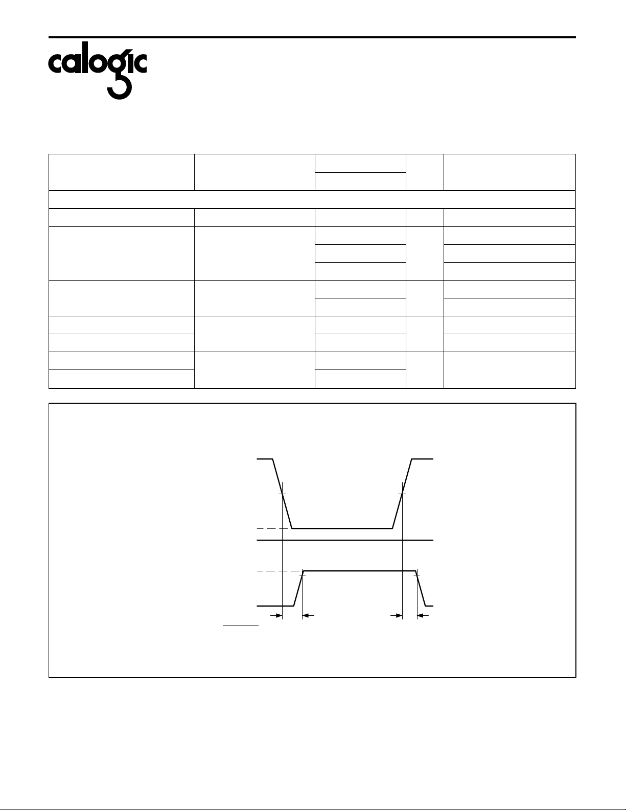
TEST WAVE FORMS
3.0V
=
A
o
C
UNITS TEST CONDITIONS
V
= -10V
S
ohm s
µA
nA
= +2.0V
S
= +10V
S
V
= +5.0V
IN
= +1 5V
IN
V
= +10V, VS = -10V
D
µA
LOGIC INPUT
t < 6nSEC
RISE
t < 4nSEC
FALL
R + r
L
R
L
0
V
0
0
DS(ON)
(V ) SWITCH INPUT
S
SWITCH OUTPUT
V =
0
()
50%
0.9
t
ON
V
S
t
OFF
Page 4

CWB308 / CWB3 09
SWICHING TIMES
-VS-
SUPPLY VOLTAGES
300
200
100
0
T = +25 C
A
o
t
on
t
off
Supply Voltages (Volts)
+5
+10
+15
Switching Time (nSec)
_
_
_
FUNCTIONAL BLOCK DIAGRAMS (1 of 4 channels)
CORPORATION
V+
IN
IL
GND
LT
CMOS CIRCUITRY
SWITCHING TIMES TEST CIRCUIT
+15V
SWITCH
INPUT
+3V
LOGIC
INPUT
R =
1K
Switch Contacts:
Switches are bi-directional (Analog Input can be to
Source or Drain. H o wever, for optimum performance i n
Video Application, connect Input to Source and Output
to Drain.
D
S
V-
DMOS SWITCH
SWITCH
OUTPUT
C = 35pF
L
Ω
L
-15V
OFF ISOLATION TEST CIRCUIT
KROHNHITE
240D
(or equivalent)
D
50
Ω
PM3214
A
B
S
50
Ω
C
OFF-ISOLATION
PHILIPS
SCOPE
(or equivalent)
C
V+
LOGIC 1 = +5V
V-
µC = 0.22 F // 10 F
OFF ISOLATION REJECTION RATIO
60
55
50
V-, V+ = +15V_
Ω
R = 50
L
45
40
µ
35
20 30 40 50 60 70 80 90 100
OIRR - OFF Isolation Rejection Ratio (db)
T = +25 C
A
o
-VS-
FREQUENCY
f - Frequency (MHz
Page 5

CORPORATION
SWITCH ON RESISTANCE
CWB308 / CWB30 9
140
V-, V+ = +15V_
R = 50Ω
120
L
T = +25 C
A
100
80
60
40
DS(on)
20
r - Switch ON Resistance (Ohms)
0
-10 -5.0 0
SWITCH ON RESISTANCE
-VS-
ANALOG VOLTAGE
o
+5.0
V - Source Voltage (Volts)
S
+10
SWITCH ON RESIST ANCE -VS- FREQUENCY TEST CIRCUIT
HP
TRACKING
GENERATOR
(or equivalent)
HP
SPECTRUM
ANALYSER
(or equivalent)
D
50
Ω
S
50
Ω
ON-RESISTANCE
SWITCH ON RESISTANCE
-VS-
SUPPLY VOLTAGES
65
60
55
Vanalog = 100mVrms
f = 1KHz
o
T = +25 C
A
Ω
R = 50
L
50
45
DS(on)
+5.0
r - Switch ON Resistance (Ohms)
__
+6.0 +8.0
__ _
+10 +12 +15_
V-, V+ - Supply Voltages (Volts)
V+
C
LOGIC 1 = +5V
µ
µC = 0.22 F // 10 F
V-
C
20MHz to 100MHz
SWITCH ON RESISTANCE
-VS-
FREQUENCY
65
V-, V+ = +8.0V_
60
55
50
DS(on)
r - Switch ON Resistance (Ohms)
20 40 60 80 100
+10V_V-, V+ =
V-, V+ =
+12V_
+15V_V-, V+ =
Ω
R = 50
L
Vanalog = 100mVrms
T = +25 C
A
o
f - Frequency (MHz)
.55
ΩSwitch ON Resistance ( /V)
.50
.45
Vanalog = 100mVrms
.40
.35
.30
20
SWITCH ON RESISTANCE
SUPPLY VOLTAGES AND FREQUENCY
+10V_V-, V+ =
Ω
R = 50
L
+12V_V-, V+ =
-VS-
o
T = +25 C
A
40 60 80 100
f - Frequency (MHz)
Page 6

CWB308 / CWB3 09
DISTORTION - VS- FREQ UENCY
CORPORATION
HP
GENERATOR
(or equivalent)
HP
SPECTRUM
ANALYSER
(or equivalent)
D
50
Ω
S
50
Ω
C
HARMONIC DISTORTION
10.0
Distortion (%)
0.05
0.02
C
V- = -15V, V+ = +15V
5.0
f = 10KHz, R = 50
2.0
1.0
0.3
0.1
V+
0.80
V-, V+ = _+15V Vanalog = 1.0Vrms
0.50
V-, V+ = _+15V Vanalog = 0.3Vrms
-VS-
0.20
0.10
o
T = +25 C
Total Harmonic Distortion (%)
o
A
0.05
10 20
LOGIC 1 = +5V
µ
µC = 0.22 F // 10 F
V-
10MHz - 40MHz
DISTORTION
ANALOG INPUT VOLTAGE
T = +25 C
Ω
L
Total Harmonic
Compensated
0.3 1.0 3.0
A
Vanalog - Analog Input (Vrms)
TOTAL HARMONIC DISTORTION
-VS-
FREQUENCY
V-, V+ = _
f - Frequency (MHz)
5.0
+10V Vanalog = 1.0Vrms
40
POWER SUPPLY REJECTION RATIO POWER SUPPL Y DECO UPLING CIRCUIT
µ
.22 F
IN
IL
LT
µ
.22 F
1K
Ω
Ω
1K
V+
90
80
S
D
V-
70
60
V- = 15V, V+ = +15V
50
V = 4.0V -f-p
MOD
Rejection Ratio (dB)
PSRR - Power Supply
40
CWB309CP
30
0.1 0.2 0.5 1.0 10.0 20
By inserting 1K ohm resistors in series with V+ and Vpower supply lines and decoupling both pins at the device
socket, it is possible to improve power supply rejection
ratios of a video switch by 50dB at frequencies of 20MHz
and higher.
POWER SUPPLY REJECTION RATIO
-PSRR, +PSRR with Decoupling
T = +25 C
A
-VS-
FREQUENCY
-PSRR
w/o Decoupling
+PSRR
o
2.0 5.0
f - Frequency (MHz)
Page 7

CORPORATION
APPLICA TIONS
LOW DISTO RTION, RAIL-T O -RAIL ANALOG SW I T CH
Features very low distortion for low frequency and large
signal applications.
CWB308 / CWB30 9
C
1
R
1
ANALOG IN
R
2
LOGIC INVERTER
R
3
RR
45
C
V+
2
+V
VERY LOW DIST ORTI ON CIRCUI T FOR LOW
FREQUENCY AND LARGE SIGNAL APPLICA TIONS
This circuit provides very low distortion ( <0.1%) and
high off isolation ( >90 dB) at signal levels equal to the
supply voltage. The si gnal passes through a T switch
configuration and at the same time is modulating the
power supply. This modulation m a inta ins a cons ta nt on
ANALOG OUT
R
6
R5 is for bypassing the power supply and has a typical
value of 1K ohm, R4 should be a value that can be
accommadat ed by the signal source as load, R3 is only
resistance r
(on) which in turn reduces the distortion.
DS
necessary at loads lower than 100 ohms and should be
selected during the initial design of the circuit, C1 has
to be large enough for the lowest signal to pass and C2
will have to bypass all signals. R1 and R2 set up the
one logic level for the control input and shou ld be set to
5 volts.
V-
-V
ANALOG IN
V+
This circuit p rovides logic inversion with two resistors
and one switch. It does not require additional logic
parts. The resistors divid e the suppl y voltage down to
R
1
ANALOG OUT
a 5 volt level when high and are switche d to a low level
via the switch. This configuration allows a single pole,
single throw switch to be changed into a single pole,
double throw switch.
5V
R
2
 Loading...