

Datasheet CT2577-11-IN-F84, CT2577-11-CG-F84, CT2577-10-XT-P119, CT2577-10-QM-P119, CT2577-10-IN-P119 Datasheet (ACT)
...Page 1

CIRCUIT TECHNOLOGY
The Future in Microelectronics
35 South Service Road · Plainview, NY 11803
TEL: 516 694-6700
· FAX: 516 694-6715
1
APPLICATION NOTE #108 Released 9/98
CT2577 / 79
SmaRT Series
Users Guide
Point of Contact:
John Vanchieri
Tel: (516) 752-2484
APPLICATION NOTE #108
Page 2

2
APPLICATION NOTE #108 Released 9/98
Table of Contents
Contents Page
Signal Descriptions...............................................................................................................................................3-7
MIL-STD-1553 Bus Interface Signals
Hard Wired Interface Signals
MIL-STD-1760 Signals
Bus Interface Signals
RT Status Word Discrete Inputs
RT Discrete Signals
BC Discrete Signals
Remote Terminal (RT) Mode............................................................................................................................. 8-21
Sequence of Operation
Receive Command
Message Illegalization
MIL-STD-1760 Features
1760 Header Word
Signals that Indicate Checksum Failure
Block Transfer Logic
READ (Receive)
DMA Transfer Times
Transmit Command
MIL-STD-1760 Features
Signals that Indicate Checksum Failure
Block Transfer Logic / DMA Transfer Times
WRITE
Changing the Status Word Bits
Device Status
Bit Register
Data Storage and Retrieval in Ram
Sample Software Code
Retriving or Loading Data to Ram
Self Test
Basic Operation
Detailed Operation
Summary of Operation
CT2577/79 RT/BT Memory Map Breakdown .................................................................................................. 22
RT/BT Device Memory Map Code Breakdown Description.....................................................................23-29
RT Status Word Control Sets
BC Control Area
RT/RX BC/TX Mode Area 00 - SA 00 (0) and BC Control
30 RT Receive / BC Transmit Subaddresses - SA 01-1E (1-30)
RT/RX BC/TX Mode Area - SA 1F (31)
RT/BC Control Area
RT/BC Block Transfer Logic (BTL) Control and Self Test Control
RT/TX BC/RX Mode Area - SA 00 (0)
30 RT Transmit / BC Receive Subaddresses -SA 01-1E (1-30)
RT/TX BC/RX Mode Area - SA 1F (31)
Broadcast RT/RX BC/TX Mode Area - SA 00 (0)
30 Broadcast RT Receive / BC Transmit Subaddresses - SA 01-1E (1-30)
Broadcast RT/RX BC/TX Mode Area 1F - SA 1F (31)
CT2577/79 Part Ordering Information .........................................................................................................30-34
CT2577 - MIL-STD-1553 / 1760 Bus Controller / Remote Terminal
CT2579 - McAir Bus Controller / Remote Terminal
CT2577/79 Pinouts...........................................................................................................................................35-41
CT2577-01-xx-F84 - 84 pin Quad Flatpack
CT2577-11-xx-F84 - 84 pin Quad Flatpack
CT2579-01-xx-F84 - 84 pin Quad Flatpack
CT2579-11-xx-F84 - 84 pin Quad Flatpack
CT2577-10-xx-P119 - 110 Pin Grid Array
CT2579-10-xx-P119 - 110 Pin Grid Array
Page 3

3
APPLICATION NOTE #108 Released 9/98
Signal Descriptions
MIL-STD-1553 Bus Interface Signals
Data0(Bus) Connect to positive side of the external databus transformer for Bus 0
Ndata0(Bus) Connect to negative side of the external databus transformer for Bus 0
Data1(Bus) Connect to positive side of the external databus transformer for Bus 1
Ndata1(Bus) Connect to negative side of the external databus transformer for Bus 1
Hard Wired Interface Signals
AddrA-E Remote Terminal address inputs for the unit. ADDR A is the least significant bit and
ADDR E is the most significant bit. RT Address inputs for the unit. AddrA is the LSB,
AddrE is the MSB.
AddrP Parity Bit for the RT Address inputs. AddrP must be set to ODD parity
MACAIR This signal sets the unit to respond with a status word within 4 uS (dead bus time)
while in Remote Terminal mode. Subaddress 1F is also enabled to be a valid
subaddress for data.
Normally subaddress 00 and 1F are reserved for mode codes.
“1" = 4 uS dead bus response time, subaddress 1F used for data.
“0" = 12 uS response time, subaddress 1F used for mode codes.
NBIT16 Select 8 or 16 bit subsystem data interface. In 8 bit mode only the lower 8 bits of the
databus (DATA 0-7) are used for all data transfers. If left open circuit the device will
default to 16 bit mode.
"0" = 16 Bit Mode
"1" = 8 Bit Mode
VME Select VME or MULTIBUS subsystem interface. If left open circuit the device will
default to VME mode.
"0" = Multibus Mode
"1" = VME Mode
*WRAPEN Select Remote Terminal wrap around to subaddress 1E. For this test to work correctly
theunit must be in RT mode. The Bus Controller sends data to subaddress 1E which
remains in the data buffer memory and is available to be sent back on the very next
command by the Bus Controller. The data in the data buffer memory in this mode
does not get transferred to the main RAM. If the very next command is not a transmit
command to subaddress 1E, the data buffer memory is flushed and will respond
normally to the next set of commands. If the wrap around test is enabled, data to
subaddress 1E must be transferred in the correct sequence.
"0" = Normal Mode
"1" = Wrap Around Mode
MIL-STD-1760 Signals
NENCHK Enables / Disables the internal hardware checksum generation and validation for both
Remote Terminal and Bus Controller. When enabled, the circuitry will check all
Page 4

4
APPLICATION NOTE #108 Released 9/98
incoming data for correct checksum and generate the correct checksum word for an
outgoing data transfer.
"0" input to this pin ENABLES the checksum circuitry.
"1" input to this pin Disables the checksum circuitry.
NVALCHK Latched version of the STATUS signal. NVALCHK is latched on the falling edge of
NCMDSTRB (RT) or NSTSTRB (BC) and will remain stable until the next
NCMDSTRB or NSTSTRB.
"0" output to this pin means the checksum was VALID.
"1" output to this pin means the checksum was NOT VALID.
STATUS Open drain output will toggle high or low on each incoming data word from the 1553
databus provided NENCHK is enabled. When the last data word is received the
STATUS line is sampled by the protocol circuitry to determine if the checksum for the
message is valid. At the end of the message, if STATUS is low then the checksum is
not valid. This STATUS signal can be wired to several different pins to customise the
units response to achecksum failure. STATUS can be wired to signals such as
NILLCMD and NSR which would cause the message to be illegalised and set Service
Request bit in the Status.
NHDR In MIL-STD-1760, the first data word of a message is defined as a Header word. The
NHDR signal indicates the presence of the Header word on the T0-T15 highway as it
is received. The user can also read the Header word from RAM.
"0" on this pin means the Header Word is on the T0-15 Bus
STREL When the store is released from the aircraft all the Remote Terminal address inputs
go high causing signal STREL to go high
LA Enables the Latched Address Option. Normally, the RT address lines are constantly
monitored and compared to the incoming Command Word. When enabled, the RT
address lines levels are internally latched every time the unit is reset. The latched RT
address information is then compared to the incoming Command Word. This latched
address function complies with the requirements of MIL-STD-1760.
"0" on this pin means the RT address lines are NOT latched
"1" on this pin means the RT address lines are latched
Bus Interface Signals
ADIN0-11 12 bit address input to the unit specifying what location the user will be access-
ing in the RAM / registers. These address inputs are inverted when the Multibus inter-
face is selected.
BCNRT Indicates what mode the unit is in.
"0" = RT Mode
"1" = BC Mode
NCARDEN Used as a Device Select. Signal to indicate the processor is addressing this unit. The
user can use this signal tied to an address decoder to enable the unit for a read/write
operation.
"0" = Enable unit for I/O operations
"1" = DISABLE unit for I/O operations
C16Mhz 16 Mhz clock system clock.
Page 5

5
APPLICATION NOTE #108 Released 9/98
DATA0-15 16 bit bidirectional data highway access to internal RAM and registers. When in 8 bit
mode only DATA 0-7 are used. Data inputs / outputs are inverted when the Multibus
interface is selected.
NACK After a write / read cycle has begun, this signal indicates that the write / read
operation to the unit has been acknowledged and that access has been granted.
Read data is available and write data is complete. The user can complete the write /
read cycle.
“0" = Cycle is acknowledged, access granted.
“1" = No acknowledge, wait.
NEMPTY Empty flag for the Command / Status FIFO memory which can store up to 32
command words (RT) or 32 status words (BC). In RT mode the memory will store all
command words that have accessed the main RAM. This includes all standard
commands to receive and transmit data from the main RAM and mode codes with
data that require subsystem involvement ie. Synchronize With Data and Transmit
Vector Word. In BC mode all status responses are stored in this memory. Access to
this memory is gained by reading from address 0 00 00.
"0" output to this pin means the FIFO is empty (no words).
"1" output to this pin means the FIFO is NOT empty (has words to be read).
NFULL Full flag for the Command / Status FIFO memory. When the signal goes low the
memoryis full and will not store any more data.
NRES Bidirectional reset pin. Interface to this pin should be in the form of an open collector
pull down driver. The unit will be reset when a low level input is asserted on power up.
The pin is bidirectional in that the unit will drive the signal out low after the status
response of the mode code Reset Remote Terminal. Upon reset the unit will initialise
to RT mode and will be able to respond immediately after the rising edge of NRES.
T0-15 16 bit bidirectional data highway access to internal RAM and registers. When in 8 bit
mode only DATA 0-7 are used. Data inputs / outputs are inverted when the Multibus
interface is selected. Allows the user to have access to the MIL-STD-1553 bus traffic
in real time. The user can utilize this bus for message illegalization and read words
such as Synch w/Data directly off the T0-15 bus. Utilizing NDATA signal, the user can
read the data words off the T0-15 bus as the DMA burst is transferring the data into
RAM.
UB Upper byte: When the unit is in 8 bit mode this signal is used as the LSB of the
address lines. In 16 bit mode the signal is not used and the LSB of the address lines
is ADIN 0.
NRD VME Mode Data Strobe for a data transfer
0 = Read/Write data
1 = Tri-state the Data 0-15 bus
Multibus Mode:Read strobe for a data transfer
0 = Read data FROM the unit TO the Subsystem
1 = Tri-state the Data0-15 bus
NWR VME Mode Read/Write direction flag for a NRD data strobe
0 = Write data FROM Subsystem TO the Device
1 = Read data FROM Device unit TO the Subsystem
Page 6

6
APPLICATION NOTE #108 Released 9/98
Multibus Mode:Write strobe for a data transfer
0 = Write data FROM the Subsystem TO the Device
1 = Tri-state the Data0-15 bus
RT Status Word Discrete Inputs
The following signals are inputs to set the appropriate bits in the RT Status word. All inputs are
sampled after the NVCR signal. These RT Status Word inputs should be latched by NVCR and
remain stable until the next NVCR signal. All the inputs listed below are active low. To set any of the
appropriate bits, the user must pull that input "low" ("0")
NME Message Error, illegalizes message. Command will not be stored in Command /
Status memory and no transfers to / from main RAM will take place. No data will be
transmitted following the status.
NTF Sets the Terminal Flag bit
NSR Sets the Service Request bit
NBUSY Sets the Subsystem Busy bit
NSSFLAG Sets the Subsystem Flag bit
NDBCA Sets the Dynamic Bus Control Accept bit in response to the Mode Code “Dynamic
Bus Control Request”
RT Discrete Signals
BCST Output high indicates command received was a broadcast. Signal will remain high until next
command is received
.
"1" = Broadcast Command was received
MCDET Output high indicates command received was a mode command. Signal will remain high until
next command is received
.
"1" = Mode Code Command was received
NCMDSTRB This signal indicates that a completely validated message has been received for
standard subaddress data activity. Mode commands with or without data will not
generate this signal. The NCMDSTRB signal is 8.5 uS long and is an indication that a
DMA burst will initiate at the end of NCMDSTRB to transfer words between the 32
word data memory and the internal main RAM. All subsystem read / writes to the
main RAM that have been acknowledged (NACK = “0") before NCMDSTRB has
begun must now be completed within 8.5 uS. All subsystem read / write requests to
the main RAM initiated after NCMDSTRB has begun will be held off (no
acknowledge) until the DMA cycle has been completed. The length of the DMA cycle
is dependant on the number of words to DMA into RAM. Access to the 32 word BTL
memory is still possible during the DMA cycle by the subsystem. However, transfers
between the BTL memory and the main RAM will be locked out.
NDBC Active low indicates that the command received by the Remote Terminal was mode
code Dynamic Bus Control. Signal will remain low until next command is received.
Page 7

7
APPLICATION NOTE #108 Released 9/98
NSYNC Signal to subsystem indicating receipt of a Synchronize mode commands If the mode
code has an associated data word, it will be available on T0-T15 at this time. If there
is no associated data word, T0-T15 will be zero.
NVCR Early indication that a Command Word has been received and is being processed.
The Command Word received is available on the T0-15 bus for decoding at this time.
The user can use this signal for message illegalization and to set the RT Status bits.
NDATA Access to valid data word in real time before being written to RAM. Data word
available on T0-T15 during active low signal.
NILLCMD Input to illegalise a command to the Remote Terminal with a clear status response.
The signal is sampled after NVCR except non mode code receive commands in
which case it is sampled after the last data word has been received. A low on this
input will illegalise the message, Command will not be stored in the Command /
Status memory and no transfers to / from main RAM will take place. The device will
respond with a clear status unless a bit has been specifically set. No data will be
transmitted following status.
BC Discrete Signals
NNEWBUS A Bus Control sequence may not normally be initiated until the current sequence is
completed, indicated by signal EOT. However, the Bus Control sequence may be
terminated and restarted if NNEWBUS is active low along with write to address 0 00
00 (000h). This feature would only be used in bus switching.
EOT Indicates that a valid transfer has been completed on the bus selected.
1 = Valid transfer completed
0 = Not yet Completed
ERROR Indication that an error has occurred either in the information transferred to the unit
from the subsystem or in the transfers on the 1553 data bus. Nature of error is
available by reading from register location 0 00 12 (012h).
1 = Error has occurred
0 = No error
NSTSTRB This signal goes low for 8.5 uS to indicate a valid transfer has been completed on the
1553 data bus and the received Status word is now available on the T0-T15 highway.
The Status word is also stored in the Command / Status memory at this time. Once
the signal goes high data received by the Bus Controller (RT to BC transfer) will be
transferred to the main RAM from the 32 word data buffer memory. Note: Data
transferred in RT to RT transfers is not stored in the Bus Controllers main RAM.
NNINHST May be used to illegalise a message just received. Signal can be tied to STATUS for
illegalisation due to 1760 checksum failures. A low will prevent any data received
being transferred to the main RAM, and the Status word will not be stored in the
Command / Status memory.
Page 8

8
APPLICATION NOTE #108 Released 9/98
Remote Terminal (RT) Mode
SEQUENCE OF OPERATION
The following section describes the sequence of operation for the various commands that
are received by the SmaRT unit in RT Mode.
RECEIVE COMMAND
An incoming command word is verified for all protocol checks (such as parity and bit count).
The verified command word is placed on the T0-15 bus and the NVCR signal is strobed. It is
at this time that a message can be illegalized.
Each successive data word after the command word is placed in an internal buffer FIFO.
This is done to double buffer the incoming data for complete message verification. Only
after the message is completely validated will the data be transferred to the internal RAM.
Otherwise, the contents of the FIFO is automatically flushed. This ensures that only valid
data will ever be read by the subsystem. The transfer from the FIFO to the RAM is
accomplished by a fast DMA burst. The guarantee of only valid data in RAM greatly
simplifies a MIL-STD-1553 RT implementation. Error handling of data is not required by the
subsystem.
The subsystem is allowed the most flexibility to access the RAM without contending with
1553 bus traffic. In 1553, data words are received at a rate of 20 µSec per word or a
maximum time of 640 µSec for a 32 word transfer. Many other systems do not buffer the
incoming data at all. That means that the RAM is periodically being updated with data words
into the RAM for up to 640 µSeconds. If an error occurs, the corrupt data is already in
memory and must be sorted out by the subsystem microprocessor. The Smart unit buffers
the data so that the RAM is completely available to the subsystem until the DMA transfer to
RAM occurs. The possibilities of memory contention is greatly reduced and the contents of
RAM is guaranteed to be valid.
When the entire set of received data words are transferred to the buffer FIFO, the
NCMDSTRB goes low indicating that a completely validated message has been received.
The received Command Word again appears on the T0-15 bus at this time. The end of the
NCMDSTRB strobe will initiate the DMA cycle to transfer the data words from the buffer
FIFO to internal RAM. The NCMDSTRB pulse is 8.5 µSec long and during this time interval,
the bus arbitration logic is active. If the subsystem has already begun a read/write operation
before NCMDSTRB, the NACK (acknowledge) signal will go low for 500 nSec allowing the
completion of the read/write command. The read/write operation must be completed within
the remaining 8 µSec. If a read/write operation starts after the NCMDSTRB strobe has
begun, the NACK will not occur and thus hold off the subsystem for the duration of the DMA
cycle to internal RAM.
During NCMDSTRB, the Command Word is loaded into the Command/Status FIFO stack
and the NEMPTY line goes high. The user can utilize this signal as an indication that some
activity has occurred. The Command/Status FIFO stores up to 32 command words for the
subsystem to review. This allows the processor to only response to the 1553 unit when
something has occurred. Constant polling of the 1553 unit is not required. To reduce
Page 9
9
APPLICATION NOTE #108 Released 9/98
processor intervention even further, the Command/Status FIFO will only store commands
that have associated data with it.
MESSAGE ILLEGALIZATION
Any message can be illegalized by applying an active low on the NME signal within 600
nSec of the rising edge of NVCR at this time. If NME signal is pulled low, the RT will respond
with a Status word having the Message Error bit set.
One way to implement this function is to place a latching PROM to the T0-T10 data bus. The
PROM would only have to decode 11 bits (5 bits subaddress, 5 bits word count, 1 bit T/R)
and have a one bit output to place a high/low level on the NME input pin. The upper five bits
(T11-T15) are just the Remote Terminal address for the unit which is a constant so no
decode of these bits are necessary. The latching signal for the PROM would be the NVCR
line. The NME pin will be read and acted upon 600 nSec after the rising edge of NVCR. The
NME signal would remain latched and stable until the next rising edge of NVCR.
MIL-STD-1760 FEATURES
To enable the 1760 features checksum validation, the NENCHK line is held low. This
enables the integrated on-chip hardware checksum features. The hardware automatically
checks the incoming message for the correct checksum.
1760 HEADER WORD
The signal NHDR will be an early indicator of the 1760 header word. This headerword will
appear on the T0-15 bus when the NHDR signal is low. The NHDR signal will go low on
every header word (first data word) even if the 1760 checksum circuitry is enabled or not.
NHDR is just an indicator of the first data word on the bus T0-15.
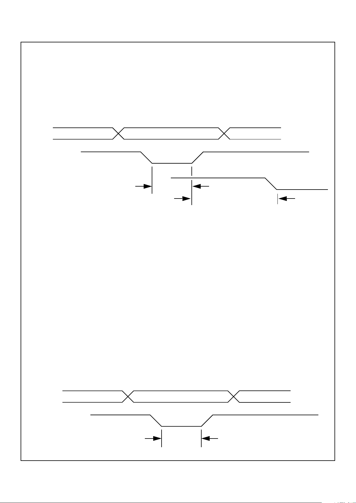
T0-15
NVCR
NME
CMD WD
500 nSec
600 nSec
Max
T0-15
NHDR
1760 HDR WD
500 nSec
Page 10

10
APPLICATION NOTE #108 Released 9/98
SIGNALS THAT INDICATE CHECKSUM FAILURE
For 1760 applications, the STATUS line indicates if a message has failed checksum. The
STATUS line will toggle up or down for each received data word as it is calculating the
checksum and is sampled on the falling edge of NCMDSTRB. The STATUS line can be tied
to any of the Status Word Bit inputs to set those bits in the event of a checksum fail. STATUS
is an open output line that will set the selected Status Word Bits for the Status Word
response in the current message. This is one of the great features for this product. The
subsystem does not have to verify the checksum in software to detect the error. The SmaRT
unit automatically does this in hardware and the unit is able to flag the error and set the a
Status Word Bit on the CURRENT Status Word response . This minimizes processor
overhead and reduces response time in notifying the Bus Controller that an error has
occurred.
For 1760 applications, the NVALCHK signal also indicates a valid checksum for the Receive
Command message. NVALCHK is a latched version of the STATUS signal and is updated
only on Receive Commands. It is valid on the falling edge of NCMDSTRB of a Receive
Command and remains stable until the next Receive Command message. A Transmit
Command message will not alter this signal because a Transmit Command does not require
an incoming checksum validation.
BLOCK TRANSFER LOGIC
The Block Transfer Logic (BTL) may be enabled for both Remote Terminal and Bus
Controller.
The BTL consists of a 32 word memory buffering the subsystem to the main RAM thus
guaranteeing data consistency for both transmit and receive transfers.
All reads and writes to the BTL are identical to read / write to the main RAM. The address
locations are the same. The only difference is that the BTL circuitry will intercept those read
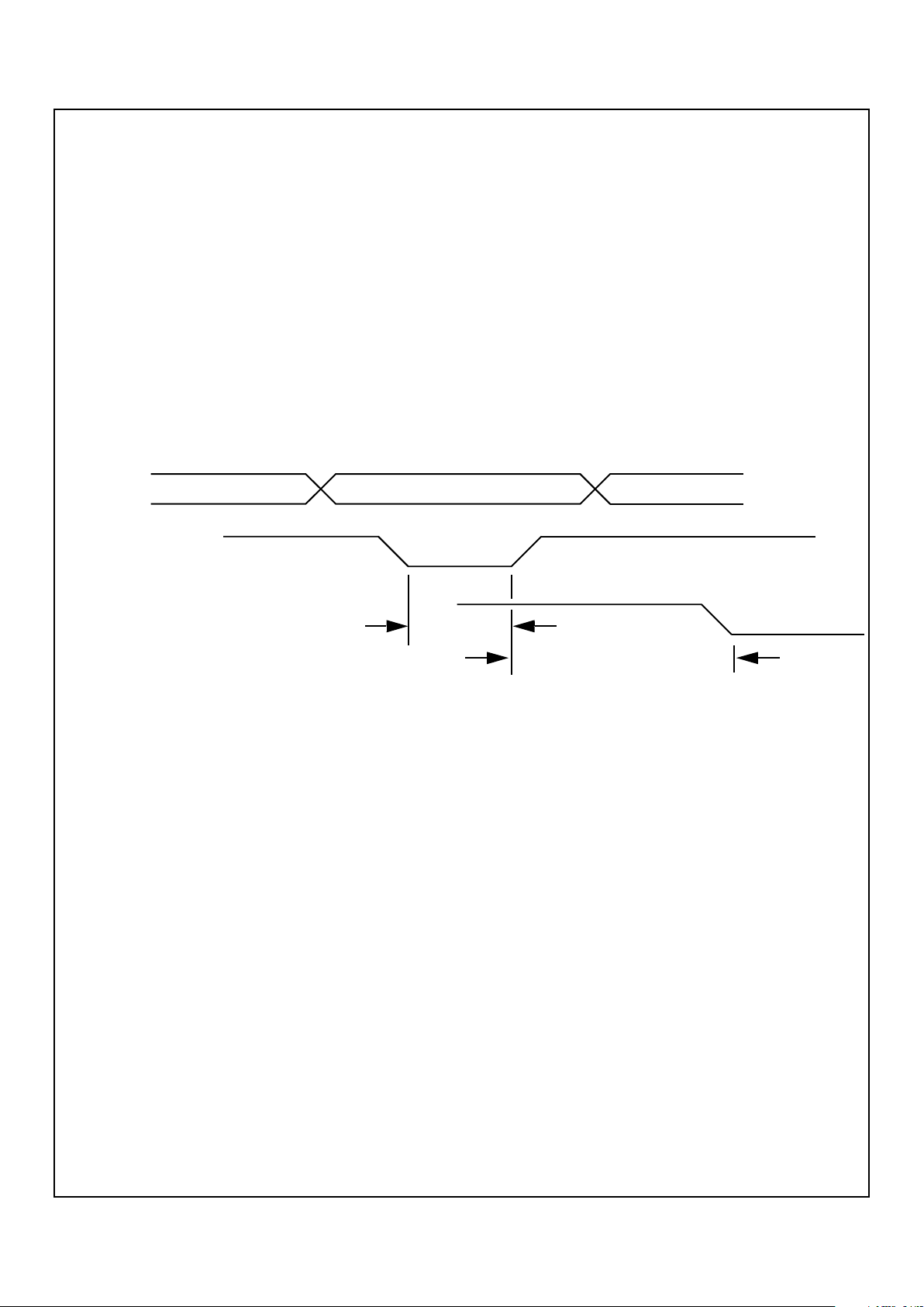
T0-15
NEMPTY
NVALCHK
CMD WD
STATUS
VALID
NCMDSTRB
Latched Until Next Receive Command
8.5 µSec
Page 11

11
APPLICATION NOTE #108 Released 9/98
/ writes and store them in the buffer instead. The user accesses the same locations as if they
would if they were directly accessing the main RAM.
The block transfer logic is enabled with signal NENBTL (pin A7) being active low and is not
applicable to subaddress 00 and 1F (unless McAir is selected) areas of ram. The block
transfer logic may also be configured by writing to certain address locations providing
NENBTL is selected, ie.
0 1 00 02 402h Disable Read Disable Write
0 1 00 03 403h Disable Read Enable Write
0 1 00 04 404h Enable Read Disable Write
0 1 00 05 405h Enable Read Enable Write
Reset will enable both Write and Read.
Note: All 257X versions with internal RAM that do not have NENBTL as a dsiscrete input
have it enabled internally.
READ (RECEIVE)
The Read BTL functions similarly to the Write BTL in that the BTL buffers the read activity. A
subsystem read will initially generate a DMA of that entire portion of the subaddress to be
stored in the BTL buffer. The subsystem can then read out the data at its leisure while the
main RAM is free for future updates. Since the entire portion of the subaddress data was
DMA from the RAM, the data read from the BTL buffer is guaranteed contiguous.
The user must read data from the device in a specific sequence starting with the first word
received in the n-1 location and ending with the last word received in location 00 of the
subaddress. The BTL will sense the read from location 00 and reset the sequence ready for
a new access.
1. The first word of a received message will be read first, this will initiate a burst DMA
transfer of a complete message from main memory to the 32 word BTL buffer memory,
during which time the subsystem will be locked out. Data is transferred at the rate of 250
ns per word.
2. The sub system can then read data from the ram at its leisure. The last word to be read
will be the last word received in the message and read from location zero. This will reset
the block transfer logic.
3. If the 1553 DMA transfer to the main RAM becomes active during the burst transfer, the
transfer will complete and then be locked out until the 1553 is complete. However the 32
word BTL buffer memory will be accessible to the subsystem at this time to read out the
data.
4. If the 1553 DMA transfer to the main RAM becomes active before the start of the burst
transfer, the transfer will belocked out until the 1553 is complete. The sub system will be
locked out during this time (main ram being accessed by the 1553 and the 32 word buffer
memory is waiting for the receive message). When the 1553 is complete the burst
transfer will take place and then unlock the subsystem.
Page 12
12
APPLICATION NOTE #108 Released 9/98
5. Once the burst transfer has commenced it will complete, thus ensuring data consistency.
DMA TRANSFER TIMES
The DMA cycle transfers words from the FIFO to internal RAM at a rate of one word each 1
µSec. The maximum DMA cycle time could possibly occur for a 32 data word transfer if the
RAM is accessed at the beginning of NCMDSTRB Strobe. Maximum subsystem hold-off
time would be 8.5 µSec (NCMDSTRB Signal) + 32 µSec (0.5 µSec per word) for a total of
24.5 µSec.
TRANSMIT COMMAND
The incoming command word is verified for all protocol checks (such as parity and bit count).
The verified command word is placed on the T0-15 bus and the NVCR signal is strobed. It is
at this time that a message can be illegalized.
Any message can be illegalized by applying an active low on the NME signal within 600
nSec of the rising edge of NVCR at this time. The RT will respond with a Status word having
the Message Error bit set. See Section 1.2.1.1 for implementing the Message Illegalization.
The NCMDSTRB goes low indicating that a completely validated message has been
received. The validated Command Word again appears on the T0-15 bus at this time. The
end of the NCMDSTRB strobe will initiate the DMA cycle to transfer the data words from
internal RAM to the buffer FIFO.
Buffering the outgoing message with a FIFO means that the subsystem is allowed the most
flexibility to access the RAM without contending with 1553 bus traffic. In 1553, data words
are transmitted at a rate of 20 µSec per word or a maximum time of 640 µSec for a 32 word
transfer. Many other systems do not buffer the outgoing data at all. That means that the
RAM is periodically being accessed for data words from the RAM for up to 640 µSeconds.
The SmaRT unit buffers the outgoing data so that the RAM is completely available to the
subsystem after the DMA transfer from RAM occurs. The possibilities of memory contention
is greatly reduced and the contents of the outgoing data will not be affected by subsystem
operations.
The NCMDSTRB pulse is 8.5 µSec long and during this time interval, the bus arbitration
logic is active. If the subsystem has already begun a read/write operation before
NCMDSTRB, the NACK (acknowledge) signal will go low for 500 nSec allowing the
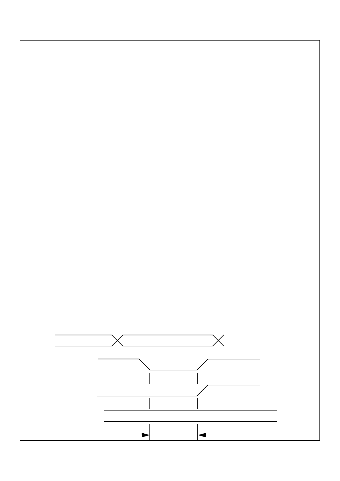
T0-15
NVCR
NME
CMD WD
500 nSec
600 nSec
Max
Page 13
13
APPLICATION NOTE #108 Released 9/98
completion of the read/write command. The read/write operation must be completed within
the remaining 8 µSec. If a read/write operation starts after the NCMDSTRB strobe has
begun, the NACK will not occur and thus hold off the subsystem for the duration of the DMA
cycle from internal RAM.
During NCMDSTRB, the Command Word is loaded into the Command/Status FIFO stack
and the NEMPTY line goes high. The user can utilize this signal as an indication that some
activity has occurred. The Command/Status FIFO stores up to 32 command words for the
subsystem to review. This allows the processor to only response to the 1553 unit when
something has occurred. Constant polling of the 1553 unit is not required. To reduce
processor intervention even further, the Command/Status FIFO will only store commands
that have associated data with it.
MIL-STD-1760 FEATURES
If the 1760 features are enabled (NENCHK line is held low), the checksum word is automatically
generated and transmitted as the last data word. The subsystem processor does not have to
calculate or load the checksum word into RAM. The SmaRT unit automatically does this in hardware
and transmits the correct checksum data word as the last word out. This reduces subsystem
processor overhead significantly.
SIGNALS THAT INDICATE CHECKSUM FAILURE
For 1760 applications, the STATUS line indicates if a message has failed checksum. The STATUS
line will stay high for a Transmit Command word because there is no associated data words received
for checksum validation. STATUS is sampled on the falling edge of NCMDSTRB. The STATUS line
can be tied to any of the Status Word Bit inputs to set those bits in the event of a checksum fail.
STATUS is an open output line that will set the selected Status Word Bits for the Status Word
response in the current message. This is one of the great features for this product. The subsystem
does not have to verify the checksum in software to detect the error. The SmaRT unit automatically
does this in hardware and the unit is able to flag the error and set the a Status Word Bit on the
CURRENT Status Word response . This minimizes processor overhead and reduces response time
in notifying the Bus Controller that an error has occurred.
For 1760 applications, the NVALCHK signal does not change from it's previous state since a Transmit
Command Word has no incoming data words. NVALCHK is a latched version of the STATUS signal
and is updated only on Receive Commands. It is valid on the falling edge of NCMDSTRB of a
Receive Command and remains stable until the next Receive Command message. A Transmit
Command message will not alter this signal because a Transmit Command does not require an
incoming checksum validation.
T0-15
NEMPTY
NVALCHK
CMD WD
PREVIOUS STATE
NCMDSTRB
8.5 µSec
* * *
* * *
Page 14

14
APPLICATION NOTE #108 Released 9/98
BLOCK TRANSFER LOGIC / DMA TRANSFER TIMES
All reads and writes to the BTL are identical to read / write to the main RAM. The address
locations are the same. The only difference is that the BTL circuitry will intercept those read
/ writes and store them in the buffer instead. The user accesses the same locations as if they
would if they were directly accessing the main RAM.
The block transfer logic may also be configured by writing to certain address locations
providing NENBTL is selected, ie.
0 1 00 02 402h Disable Read Disable Write
0 1 00 03 403h Disable Read Enable Write
0 1 00 04 404h Enable Read Disable Write
0 1 00 05 405h Enable Read Enable Write
Reset will enable both Write and Read.
WRITE
The Write BTL Logic basically stores all writes to a particular subaddress in the buffer until
the subsystem has completed the entire subaddress update. When the subsystem has
finished, the BTL will generate a burst DMA from the BTL to main RAM in one contiguous
transfer. This guarantees that the entire subaddress is updated. Until the DMA transfer the
BTL buffer allows the main RAM to be free for updates from the 1553 data bus.
The user must write data to the device in a specific sequence starting with the first word for
transmission in the n-1 location and ending with the last word for transmission in location 00
of the subaddress. The BTL will sense the write to location 00 and initiate the DMA
sequence.
1. Data for one message is written to the 32 word buffer memory at any speed by the
subsystem. The first word for transmission is written first to the n-1 location and the last
word for transmission is written last to the 00 location of the subaddress.
2. The address of the first word is stored in a register / counter within the "block transfer
logic".
3. The last word for transmission is always written to location zero, this will trigger the
transfer of data from the 32 word buffer memory to the main memory. Data is transferred
at the rate of 250 nS per word. A full 32 word transfer will take approximately 8 uS.
4. If the 1553 is quiet the entire message will immediately be transferred in a single burst to
the main memory, the address being generated by the counter within the block transfer
logic. During this transfer the subsystem will be locked out via NACK from any new
updates.
5. If the 1553 DMA transfer to the main RAM becomes active during the burst transfer, the
transfer will complete and then be locked out of any new updates until the 1553 is
complete. However the BTL buffer memory will be accessible to the subsystem at this
time.
6. If the 1553 DMA transfer to the main RAM becomes active before the start of the burst
transfer, the transfer will be locked out (after location zero is written to) until the 1553 is
complete. The sub system will be locked out during this time (main ram being accessed
Page 15

15
APPLICATION NOTE #108 Released 9/98
by the 1553 and the BTL buffer memory is full). If the BTL memory is not fully loaded, the
subsystem can continue to load the BTL memory until full (write to 00 indicates a full
condition). When the 1553 is complete the burst transfer will take place and then unlock
the subsystem.
7. Once the burst transfer has commenced it will complete, thus ensuring data consistency.
The DMA cycle begins after the rising edge of NCMDSTRB. All requested data words are
placed in an internal buffer FIFO. This is done to double buffer the outgoing data as a
contiguous block and free up the internal RAM as quickly as possible. The DMA cycle
transfers words from internal RAM at a rate of one word each 1 µSec. The maximum DMA
cycle time would occur for a 32 data word transfer or 32 µSec. Maximum subsystem hold-off
time would be 8.5µSec + 32 µSec for a total of 40.5 µSec.
CHANGING THE STATUS WORD BITS
There are four Status word bits that can be altered by the subsystem through simple write
operations. These four bits and addresses are as follows:
SERVREQ 0 0 00 08 008h
BUSY 0 0 00 04 004h
SSFLAG 0 0 00 02 002h
DBCA 0 0 00 01 001h
See Memory Map for further details.
DEVICE STATUS
The status of the device may be determined by reading from location 0 00 01, the status bits
and BTL status will be available on DATA pins 0-7.
DATA0 DBCA
DATA1 SSFLAG
DATA2 SSBUSY
DATA3 SERVREQ
DATA4 BTL WRITE ENABLED
DATA5 BTL READ ENABLED
DATA6 OFF-LINE SELF TEST ENABLED
DATA7 ON-LINE SELF TEST ENABLED
See Memory Map for further details.
BIT REGISTER
With MCAIR (pin F1) disabled, writing data to 0 1 00 13 or 0 1 1F 13 will set the content of
the BIT register. The data may also be read from these locations. This register is
non-resetable. See Memory Map for further details.
Page 16

16
APPLICATION NOTE #108 Released 9/98
DATA STORAGE AND RETRIEVAL IN RAM
The storage and retrieval of data on RAM is optimized for fast processor accesses. The
data (Transmit or Receive) is stored with the first data word (Word #0) in memory location
#0n and the last data word (Word #n) in location 00. The processor reads the Command
word and extracts the T/R bit, subaddress, and word count bits as a pointer to the proper
memory location. The word count field is used as a down counter variable so that a Do Loop
routine is executed and then branched out at counter = 00. This may be more efficient in
some compilers than an up counter and comparing current loop counter with word count
field on every loop. The following section contains sample software pseudo code for data
handling. See Memory Map for further details.
SAMPLE SOFTWARE CODE
The following section contains sample pseudo-code for programming and operation the
SmaRT unit. The code most resembles Microsoft Quick Basic code (IBM DOS compatible)
for simplicity.
RETRIEVING OR LOADING DATA TO RAM
REM *******************************************************************************************
REM *
REM * Routines for operation in Remote Terminal (RT) Mode
REM *
REM ********************************************************************************************
REM ********************************************************************************************
REM * Variables
REM * _______
REM *
REM * NCMDEMPTY 0 = EMPTY (NO Command WORDS IN FIFO)
REM * 1 = HAVE COMMAND WORDS IN FIFO
REM *
REM * This signal is derived from NEMPTY
REM * on the CT2577.
REM *
REM * MODE 0 = RT MODE
REM * 1 = BC MODE
REM *
REM * CMDWORD = COMMAND WORD READ FROM FIFO
REM *
REM * WORDCNT = LOWER 5 BIT OF COMMAND WORD
REM * INDICATES HOW MANY DATA WORDS
REM *
REM * DATA() = DATA ARRAY (32 WORDS MAX)
REM *
REM * MEMPOINT = LOWER 11 BITS OF THE COMMAND WORD
REM *
REM * T/R_BIT = BIT #10 OF THE COMMAND WORD
REM *
REM *
Page 17

17
APPLICATION NOTE #108 Released 9/98
REM *
REM *
REM *******************************************************************************************
REM********************************************************************************************
REM ************ INITIALIZATION ROUTINE
***********************************************
REM *******************************************************************************************
INIT: DEFINT A-Z
OUT 1, 400(h) "WRITE TO THIS ADDRESS TO SET CT2577 INTO RT MODE
INPUT MODE, XX(h) "READ PIN BCNRT FROM THE CT2577
" 0 = RT MODE
" 1 = BC MODE
DIM DATA(32) "LOCATIONS 1-32 = 32 WORDS
REM ******************************************************************************************
REM ******************************************************************************************
REM ************ DETECT COMMAND ROUTINE ****************************************
REM ******************************************************************************************
DETECT: IF NCMDEMPTY = 1 THEN
CMDWORD = INPUT(OOh) ;READ FROM LOCATION 00
MEMPOINT = CMDWORD & 0000011111111111(b)
T/R_BIT = CMDWORD & 0000010000000000(b)
WORDCNT = CMDWORD & 0000000000011111(b)
MEMPOINT = MEMPOINT - 1
"OFFSET POINTER SO THAT FINAL POSITION
"IS AT LOCATION 00. FOR EXAMPLE, A ONE
"WORD TRANSFER SHOULD BE LOADED IN
"LOCATION 00 OF THAT SUBADDRESS.
END IF
IF WORDCNT = 00000(b) THEN
WORDCNT = 32 "ALL ZEROS IN WORD COUNT FIELD = 32 DATA WORDS
END IF
IF T/R_BIT = 0000000000000000(b) THEN
REDIM DATA() ;CLEARS ARRAY DATA()
; GOT TO ROUTINE TO READ OUT
; THE RECEIVED DATA FROM THE 1553 BUS
GOTO RECEIVE
END IF
IF T/R_BIT = 0000010000000000(b) THEN
REDIM DATA() ;CLEARS ARRAY DATA()
FOR J = 1 TO 32
Page 18

18
APPLICATION NOTE #108 Released 9/98
DATA(J) = XXXX ;LOAD IN DATA FOR TRANSMIT
NEXT J
GOTO TRANSMIT
END IF
GOTO END
REM ***********************************************************************************************
REM *** ROUTINE TO LOAD DATA INTO RAM FROM PROCESSOR *************************
REM ***********************************************************************************************
TRANSMIT: FOR I = 1 TO WORDCNT
OUTPUT DATA(I), MEMPOINT ; WRITES DATA() INTO LOCATION
; MEMPOINT
MEMPOINT = MEMPOINT - 1
NEXT I
GOTO END
REM
******************************************************************************************************
REM *** ROUTINE TO READ DATA FROM RAM TO PROCESSOR
********************************
REM
******************************************************************************************************
RECEIVE: FOR I = 1 TO WORDCNT
DATA(I) = INPUT(MEMPOINT) ; READS LOCATION MEMPOINT INTO
; DATA() ARRAY
MEMPOINT = MEMPOINT - 1
NEXT I
GOTO END
REM
******************************************************************************************************
REM *** ROUTINE TO SCAN FOR MORE MESSAGES
****************************************
REM
******************************************************************************************************
END: IF NCMDEMPTY = 1 THEN
GOTO DETECT
ELSE
RETURN
; GO OFF AND DO SOMETHING ELSE
; UNTIL ANOTHER 1553 MESSAGE IS RECEIVED
END IF
Page 19

19
APPLICATION NOTE #108 Released 9/98
SELF TEST
The self test feature is an internal and external loop back test for additional verification of
functionality. This is in addition to the Remote Terminal Wraparound circuitry. The difference
is that this test is manual and under subsystem control. The subsystem microprocessor
initiates the self test and the subsequent data word pattern. The subsystem then reads back
the wrapped data word and determines if it is correct. The online self test must be done with
the 1553 data bus quiet.
The self test function is enabled or disabled by writing to certain address locations. Reset
will disable self test.
0 1 00 06 Enable offline self test and set device status bit 6
0 1 00 07 Enable online self test and set device status bit 7
0 1 00 08 Disable self test
When self test is enabled the device is set up as both BC and RT. When self test is disabled
the device will revert back to its previous state.
BASIC OPERATION
The basic operation is for the BC to transmit the message "receive one data word" and for
the RT to receive this message.
If the online self test is selected the message will be transmitted onto the 1553 bus via the
transceivers and be received by the RT via transceivers. The RT will not respond with
Status.
If the offline self test is selected the transceivers will be inhibited and the Manchester
encoder output is routed to the Manchester decoder input.
The status of the device may be obtained by reading from 0 0 00 01. Bit 6 is offline self test
enabled. Bit 7 is online self test enabled.
DETAILED OPERATION
1. Enable self test by writing to either 1 00 06 (offline) or 0 1 00 07 (online).
2. Select required 1553 data bus to be tested by writing to 0 0 00 10 or 0 0 00 18.
3. Write the data word contents required for the self test to the appropriate RAM location ie. For
broadcast message: 2(bcast) 01-1E(subaddress) 00(1 word) or normal receive message: 0(rec)
01-1E(subaddress) 00(1 word).
4. Initiate BC to RT transfer of one data word by writing to address 0 00 00 with a data word content
of 1F or RTaddr 0(rec) 01-1E(subaddress) 01(1 data word). The following automatic sequence is
now initiated:
a) The Command word (data word written to location 0 0 00 00) is processed by the BC protocol,
transferred to the Manchester encoder and transmitted onto the bus (online self test) or to the
Manchester decoder (offline self test).
Page 20

20
APPLICATION NOTE #108 Released 9/98
b) The self test data word is read from the appropriate RAM location, transferred to the encoder
and transmitted contiguously following the command word.
c) The Command word is received by the Manchester decoder, if valid and with correct RT
address or broadcast is stored in the RT protocol.
d) The data word is received by the decoder and if valid is stored in the 32 word data memory.
e) The RT protocol will validate the message and if successful will write the Command word to
the 32 word Command / Status memory and transfer the data word to the appropriate RAM
location.
5. As the data word received is written to the same RAM location that it was originally accessed
from, the contents should be altered while the self test is in progress (eg. write 0000). This can be
done immediately after the BC to RT transfer was initiated. There is approx 45 us for the self test
to complete.
6. To ensure that the RAM contents have been altered it is advisable to read the data back from the
RAM.
7. On completion of a successful self test the signal NCMDSTRB will go active low, after which the
data can be read from the RAM and compared with the data used in the self test.
8. In addition the Command word used in the self test may be read from 0 00 00.
9. Disable self test by writing to 1 00 08. The device will revert back to its original state (BC or RT).
Page 21

21
APPLICATION NOTE #108 Released 9/98
SUMMARY OF OPERATION
Device can be either RT or BC.
1. ADDR = 1 00 06 (Write) Select offline self test.
OR
ADDR = 1 00 07 (Write) Select online self test.
2. ADDR = 1 00 10 (Write) Select bus 0.
OR
ADDR = 1 00 18 (Write) Select bus 1.
3. ADDR = 2 01-1E 00 (Write) DATA = n Write self test data to BCAST location.
OR
ADDR = 0 01-1E 00 (Write) DATA = n Write self test data to RECEIVE location.
4. ADDR = 0 00 00 (Write) DATA = 1F 0 01-1E 01 Transmit message (Bcast receive 1 word).
OR
ADDR = 0 00 00 (Write) DATA = RTAD 0 01-1E 01 Transmit message (Receive 1 word).
5. ADDR = 2 01-1E 00 (Write) DATA = 0 Write 0 to self test location.
OR
ADDR = 0 01-1E 00 (Write) DATA = 0 Write 0 to self test location.
6. ADDR = 2 01-1E 00 (Read) DATA = 0 Read 0 from self test location.
OR
ADDR = 0 01-1E 00 (Read) DATA = 0 Read 0 from self test location.
7. ADDR = 2 01-1E 00 (Read) DATA = n Read self test data after NCMDSTRB.
OR
ADDR = 0 01-1E 00 (Read) DATA = n Read self test data after NCMDSTRB.
8. ADDR = 0 00 00 (Read) DATA = 1F 0 01-1E 01 Read command from command memory.
OR
or ADDR = 0 00 00 (Read) DATA = RTAD 0 01-1E 01 Read command from command memory.
9. ADDR = 1 00 08 (Write) Disable self test.
ADDR = 0 00 01 (Read) Read device status:
Bit 6 = Offline self test.
Bit 7 = Online self test
Page 22

22
APPLICATION NOTE #108 Released 9/98
CT2577 /79 RT/BC Device Memory Map Breakdown
The following description is for devices that have internal 3K memory.
ALL 'User' Locations are Read/Writable
BCST (Binary)
T/R (Binary)
Subaddress (Hex)
Word Count (Hex)
Composite VME Address 16-bit mode (Hex)
Composite VME Address 8-bit mode (Hex) = Lower Byte
Upper Byte = Address +1
Composite MULTIbus Address 16-bit mode (Hex)
FUNCTION
0 0 00 00 000 0000 FFF W - Command Word (2nd RT-RT Command) (BC)
TRIGGERS BC - BUS ’X’ Operation
R - Received STATUS (FIFO Stack) (BC)
W - Resets ALL Status Bits (RT)
R - RT Received COMMAND (RT)
0 0 00 01 001 0002 FFE
R/W - 1st RT-RT COMMAND (BC)
R/W - Memory Address 002 through 00Fh (BC)
W - Sets STATUS Word Flags as Described below (RT)
R - ALL Status Bits WRITTEN (RT) via Addresses 001---
00F plus BURST Control as Follows:
x = Don't Care
Y = STATUS Word Bits Selected via WRITEs to 001 through 00Fh
B = BURST Control Selected via WRITEs to 402 through 405h
xxxx xxxx 00 B B Y Y Y Y
DBC
SSF
BUSY
SR
BTL WRITE ENABLED (TX)
BTL READ ENABLED (RX)
Page 23

23
APPLICATION NOTE #108 Released 9/98
RT/BC Device Memory Map Code Breakdown Descriptions
RT STATUS WORD Control Sets
0 0 00 01 001 0002 FFFE DBC
0 0 00 02 002 0004 FFFD SSFLAG
0 0 00 03 003 0006 FFFC SSFLAG + DBC
0 0 00 04 004 0008 FFFB BUSY
0 0 00 05 005 000A FFFA BUSY + DBC
0 0 00 06 006 000C FFF9 BUSY + SSFLAG
0 0 00 07 007 000E FFF8 BUSY + SSFLAG + DBC
0 0 00 08 008 0010 FFF7 SERVREQ
0 0 00 09 009 0012 FFF6 SERVREQ + DBC
0 0 00 0A 00A 0014 FFF5 SERVREQ + SSFLAG
0 0 00 0B 00B 0016 FFF4 SERVREQ + SSFLAG + DBC
0 0 00 0C 00C 0018 FFF3 SERVREQ + BUSY
0 0 00 0D 00D 001A FFF2 SERVREQ + BUSY + DBC
0 0 00 0E 00E 001C FFF1 SERVREQ + BUSY + SSFLAG
0 0 00 0F 00F 001E FFF0 SERVREQ + BUSY + SSFLAG + DBC
BC Control Area
0 0 00 10 010 0020 FFEF BC - SELECT BUS 0
(18 018 0040 FFE7BC - SELECT BUS 1)
RT/RX BC/TX Mode Area 00 - SA 00 (0) and BC Control
0 0 00 11 011 0022 FFEE SYNC WORD
0 0 00 12 012 0024 FFED ERROR Register
0 0 00 13 013 0026 FFEC User
0 0 00 14 014 0028 FFEB SELECTED TX SHUTDOWN (0000/0001)
0 0 00 15 015 002A FFEA OVERRIDE SELECTED TX SHUTDOWN (0000/0001)
0 0 00 16 016 002C FFE9 User
0 0 00 17 017 002E FFE8 User
0 0 00 18 018 0030 FFE7 BC - SELECT BUS 1
(10 010 0020 FFEF BC - SELECT BUS 0)
0 0 00 19 019 0032 FFE6 User
THROUGH
0 0 00 1F 01F 003E FFE0 User
30 RT Receive / BC Transmit Subaddresses - SA 01-1E (1-30)
0 0 01 00 020 0040 FFDF SA1Last Word (Word 01 if WC =1)
0 0 01 04 024 0048 FFDB Word 01 if WC = 5
0 0 01 1F 03F 007E FFC0 Word 01 if WC = 32
0 0 02 00 040 0080 FFBF SA2
0 0 02 1F 05F 00BE FFA0
0 0 03 00 060 00C0 FF9F SA3
Page 24

24
APPLICATION NOTE #108 Released 9/98
0 0 03 1F 07F 00FE FF80
0 0 04 00 080 0100 FF7F SA4
0 0 04 1F 09F 013E FF60
0 0 05 00 0A0 0140 FF5F SA5
0 0 05 1F 0BF 017E FF40
0 0 06 00 0C0 0180 FF3F SA6
0 0 06 1F 0DF 01BE FF20
0 0 07 00 0E0 01C0 FF1F SA7
0 0 07 1F 0FF 01FE FF10
0 0 08 00 100 0200 FEFF SA8
0 0 08 1F 11F 023E FEE0
0 0 09 00 120 0240 FEDF SA9
0 0 09 1F 13F 027E FEC0
0 0 0A 00 140 0280 FEBF SA10
0 0 0A 1F 15F 02BE FEA0
0 0 0B 00 160 02C0 FE9F SA11
0 0 0B 1F 17F 02FE FE80
0 0 0C 00 180 0300 FE7F SA12
0 0 0C 1F 19F 033E FE60
0 0 0D 00 1A0 0340 FE5F SA13
0 0 0D 1F 1BF 037E FE40
0 0 0E 00 1C0 0380 FE3F SA14
0 0 0E 1F 1DF 03BE FE20
0 0 0F 00 1E0 03C0 FE1F SA15
0 0 0F 1F 1FF 03FE FE00
0 0 10 00 200 0400 FDFF SA16
0 0 10 1F 21F 043E FDE0
0 0 11 00 220 0440 FDDF SA17
0 0 11 00 23F 047E FDC0
0 0 12 00 240 0480 FDBF SA18
0 0 12 1F 25F 04BE FDA0
0 0 13 00 260 04C0 FD9F SA19
0 0 13 1F 27F 04FE FD80
0 0 14 00 280 0500 FD7F SA20
0 0 14 1F 29F 053E FD60
0 0 15 00 2A0 0540 FD5F SA21
0 0 15 1F 2BF 057E FD40
0 0 16 00 2C0 0580 FD3F SA22
0 0 16 1F 2DF 05BE FD20
0 0 17 00 2E0 05C0 FD1F SA23
0 0 17 1F 2FF 05FE FD00
0 0 18 00 300 0600 FCFF SA24
0 0 18 1F 31F 063E FCE0
0 0 19 00 320 0640 FCDF SA25
0 0 19 1F 33F 067E FCC0
0 0 1A 00 340 0680 FCBF SA26
0 0 1A 1F 35F 06BE FCA0
0 0 1B 00 360 06C0 FC9F SA27
0 0 1B 1F 37F 06FE FC80
Page 25

25
APPLICATION NOTE #108 Released 9/98
0 0 1C 00 380 0700 FC7F SA28
0 0 1C 1F 39F 073E FC60
0 0 1D 00 3A0 0740 FC5F SA29
0 0 1D 1F 3BF 077E FC40
0 0 1E 00 3C0 0780 FC3F SA30
0 0 1E 1F 3DF 07BE FC20
RT/RX BC/TX Mode Area - SA 1F (31)
0 0 1F 00 3E0 07C0 FC1F User
THROUGH
0 0 1F 10 3F0 07E0 FC0F User
0 0 1F 11 3F1 07E2 FC0E SYNC WORD
0 0 1F 12 3F2 07E4 FC0D User
0 0 1F 13 3F3 07E6 FC0C User
0 0 1F 14 3F4 07E8 FC0B SELECTED TX SHUTDOWN (0000/0001)
0 0 1F 15 3F5 07EA FC0A OVERRIDE SELECTED TX SHUTDOWN (0000/0001)
0 0 1F 16 3F6 07EC FC09 User
THROUGH
0 0 1F 1F 3FF 07FE FC00 User
RT/BC Control Area
0 1 00 00 400 0800 FBFF SELECT RT
0 1 00 01 401 0802 FBFE SELECT BC
RT/BC Block Transfer Logic (BTL) Control and Self Test Control
0 1 00 02 402 0804 FBFD RX BTL OFF / TX BTL OFF
0 1 00 03 403 0806 FBFC RX BTL OFF / TX BTL ON
0 1 00 04 404 0808 FBFB RX BTL ON / TX BTL OFF
0 1 00 05 405 080A FBFA RX BTL ON / TX BTL ON
0 1 00 06 406 080C FBF9 OFF- LINE Self Test
0 1 00 06 407 080E FBF8 ON-LINE Self Test
0 1 00 06 408 0810 FBF7 DISABLE Self Test
0 1 00 06 409 0812 FBF6 User
THROUGH
0 1 00 0F 40F 081E FBF0 User
RT/TX BC/RX Mode Area - SA 00 (0)
0 1 00 10 410 0820 FBEF VECTOR WORD
0 1 00 11 411 0822 FBDF User
0 1 00 12 412 0824 FBCF LAST COMMAND
0 1 00 13 413 0826 FBBF BIT WORD
0 1 00 14 414 0828 FBAF User
THROUGH
0 1 00 1F 41F 083E FBE0 User
Page 26

26
APPLICATION NOTE #108 Released 9/98
30 RT Transmit / BC Receive Subaddresses - SA 01-1E (1-30)
0 1 01 00 420 0840 FBDF SA1 Last Word (Word 01 if WC =1)
0 1 01 04 424 0848 FBDB SA1 Word 01 if WC = 5
0 1 01 1F 43F 087E FBC0 SA1 Word 01 if WC = 32
0 1 02 00 440 0880 FBBF SA2
0 1 02 1F 45F 08BE FBA0
0 1 03 00 460 08C0 FB9F SA3
0 1 03 1F 47F 08FE FB80
0 1 04 00 480 0900 FB7F SA4
0 1 04 1F 49F 093E FB60
0 1 05 00 4A0 0940 FB5F SA5
0 1 05 1F 4BF 097E FB40
0 1 06 00 4C0 0980 FB3F SA6
0 1 06 1F 4DF 09BE FB20
0 1 07 00 4E0 09C0 FB1F SA7
0 1 07 1F 4FF 09FE FB00
0 1 08 00 500 0A00 FAFF SA8
0 1 08 1F 51F 0A3E FAE0
0 1 09 00 520 0A40 FADF SA9
0 1 09 1F 53F 0A7E FAC0
0 1 0A 00 540 0A80 FABF SA10
0 1 0A 1F 55F 0ABE FAA0
0 1 0B 00 560 0AC0 FA9F SA11
0 1 0B 1F 57F 0AFE FA80
0 1 0C 00 580 0B00 FA7F SA12
0 1 0C 1F 59F 0B3E FA60
0 1 0D 00 5A0 0B40 FA5F SA13
0 1 0D 1F 5BF 0B7E FA40
0 1 0E 00 5C0 0B80 FA3F SA14
0 1 0E 1F 5DF 0BBE FA20
0 1 0F 00 5E0 0BC0 FA1F SA15
0 1 0F 1F 5FF 0BFE FA00
0 1 10 00 600 0C00 F9FF SA16
0 1 10 1F 61F 0C3E F9E0
0 1 11 00 620 0C40 F9DF SA17
0 1 11 00 63F 0C7E F9C0
0 1 12 00 640 0C80 F9BF SA18
0 1 12 1F 65F 0CBE F9A0
0 1 13 00 660 0CC0 F99F SA19
0 1 13 1F 67F 0CFE F980
0 1 14 00 680 0D00 F97F SA20
0 1 14 1F 69F 0D3E F960
0 1 15 00 6A0 0040 F95F SA21
0 1 15 1F 6BF 0D7E F940
0 1 16 00 6C0 0D80 F93F SA22
0 1 16 1F 6DF 0DBE F920
0 1 17 00 6E0 0DC0 F91F SA23
Page 27

27
APPLICATION NOTE #108 Released 9/98
0 1 17 1F 6FF 0DFE F900
0 1 18 00 700 0E00 F8FF SA24
0 1 18 1F 71F 0E3E F8E0
0 1 19 00 720 0E40 F8DF SA25
0 1 19 1F 73F 0E7E F8C0
0 1 1A 00 740 0E80 F8BF SA26
0 1 1A 1F 75F 0EBE F8A0
0 1 1B 00 760 0EC0 F89F SA27
0 1 1B 1F 77F 0EFE F880
0 1 1C 00 780 0F00 F87F SA28
0 1 1C 1F 79F 0F3E F860
0 1 1D 00 7A0 0F40 F85F SA29
0 1 1D 1F 7BF 0F7E F840
0 1 1E 00 7C0 0F80 F83F SA30
0 1 1E 1F 7DF 0FBE F820
RT/ TX BC/RX Mode Area - SA 1F (31)
0 1 1F 00 7E0 0FC0 F81F
THROUGH
0 1 1F 0F 7EF 0FDE F810
0 1 1F 10 7F0 0FE0 F80F VECTOR WORD
0 1 1F 11 7F1 0FE2 F80E User
0 1 1F 12 7F2 0FE4 F80D LAST COMMAND
0 1 1F 13 7F3 0FE6 F80C BIT WORD
0 1 1F 14 7F4 0FE8 F80B User
THROUGH
0 1 1F 1F 7FF 0FFE F800 User
Broadcast RT/RX BC/TX Mode Area - SA 00 (0)
1 0 00 00 800 1000 F7FF User
THROUGH
1 0 00 10 810 1020 F7EF User
1 0 00 11 811 1022 F7EE SYNC WORD
1 0 00 12 812 1024 F7ED User
1 0 00 13 813 1036 F7EC User
1 0 00 14 814 1028 F7EB SELECTED TX SHUTDOWN (0000/0001)
1 0 00 15 815 102A F7EA OVERRIDE SELECTED TX SHUTDOWN (0000/0001)
1 0 00 16 816 102C F7E9 User
THROUGH
1 0 00 1F 81F 103E F7E0 User
30 Broadcast RT Receive / BC Transmit Subaddresses - SA 01-1E (1-30)
1 0 01 00 820 1040 F7DF SA1 Last Word (Word 01 if WC =1)
1 0 01 04 824 1048 F7DB SA1 Word 01 if WC = 5
1 0 01 1F 83F 107E F7C0 SA1 Word 01 if WC = 32
1 0 02 00 840 1080 F7BF SA2
1 0 02 1F 85F 10BE F7A0
Page 28

28
APPLICATION NOTE #108 Released 9/98
1 0 03 00 860 10C0 F79F SA3
1 0 03 1F 87F 10FE F780
1 0 04 00 880 1100 F77F SA4
1 0 04 1F 89F 113E F760
1 0 05 00 8A0 1140 F75F SA5
1 0 05 1F 8BF 117E F740
1 0 06 00 8C0 1180 F73F SA6
1 0 06 1F 8DF 11BE F720
1 0 07 00 8E0 11C0 F71F SA7
1 0 07 1F 8FF 11FE F700
1 0 08 00 900 1200 F6FF SA8
1 0 08 1F 91F 123E F6E0
1 0 09 00 920 1240 F6DF SA9
1 0 09 1F 93F 127E F6C0
1 0 0A 00 940 1280 F6BF SA10
1 0 0A 1F 95F 12BE F6A0
1 0 0B 00 960 12C0 F69F SA11
1 0 0B 1F 97F 12FE F680
1 0 0C 00 980 1300 F67F SA12
1 0 0C 1F 99F 133E F660
1 0 0D 00 9A0 1340 F65F SA13
1 0 0D 1F 9BF 137E F640
1 0 0E 00 9C0 1380 F63F SA14
1 0 0E 1F 9DF 13BE F620
1 0 0F 00 9E0 13C0 F61F SA15
1 0 0F 1F 9FF 133E F600
1 0 10 00 A00 1400 F5FF SA16
1 0 10 1F A1F 143E F5E0
1 0 11 00 A20 1440 F5DF SA17
1 0 11 00 A3F 147E F5C0
1 0 12 00 A40 1480 F5BF SA18
1 0 12 1F A5F 14BE F5A0
1 0 13 00 A60 14C0 F59F SA19
1 0 13 1F A7F 14FE F580
1 0 14 00 A80 1500 F57F SA20
1 0 14 1F A9F 153E F560
1 0 15 00 AA0 1540 F55F SA21
1 0 15 1F ABF 157E F540
1 0 16 00 AC0 1580 F53F SA22
1 0 16 1F ADF 15BE F520
1 0 17 00 AE0 15C0 F51F SA23
1 0 17 1F AFF 15FE F500
1 0 18 00 B00 1600 F4FF SA24
1 0 18 1F B1F 163E F4E0
1 0 19 00 B20 1640 F4DF SA25
1 0 19 1F B3F 167E F4C0
1 0 1A 00 B40 1680 F4BF SA26
1 0 1A 1F B5F 16BE F4A0
1 0 1B 00 B60 16C0 F49F SA27
Page 29

29
APPLICATION NOTE #108 Released 9/98
1 0 1B 1F B7F 16FE F480
1 0 1C 00 B80 1700 F47F SA28
1 0 1C 1F B9F 173E F460
1 0 1D 00 BA0 1740 F45F SA29
1 0 1D 1F BBF 177E F440
1 0 1E 00 BC0 1780 F43F SA30
1 0 1E 1F BDF 17BE F420
Broadcast RT/RX BC/TX Mode Area 1F - SA 1F (31)
1 0 1F 00 BE0 17C0 F41F User
THROUGH
1 0 1F 10 BF0 17E0 F40F User
1 0 1F 11 BF1 17E2 F40E SYNC WORD
1 0 1F 12 BF2 17E4 F40D User
1 0 1F 13 BF3 17E6 F40C User
1 0 1F 14 BF4 17E8 F40B SELECTED TX SHUTDOWN (0000/0001)
1 0 1F 15 BF5 17EA F40A OVERRIDE SELECTED TX SHUTDOWN (0000/0001)
1 0 1F 16 BF6 17EC F409 User
THROUGH
1 0 1F 1F BFF 17FE F400 User
Page 30

30
APPLICATION NOTE #108 Released 9/98
CT2577 / 79 Part Ordering
Information
Page 31

31
APPLICATION NOTE #108 Released 9/98
CT2577 - Mil-Std 1553 / 1760 Bus Controller/Remote
Terminal
CT2577- XX- YY-ZZ
P 119 = 119 Pin PGA
F 84 = 84 Pin Quad Flatpack
QM = Full Mil 883C Screened Part (-55
0
C to +1250C)
XT = Extended Temperature Range (-55
0
C to +1250C)
I N = Industrial Temperature Range (-40
0
C to +850C)
CG = Commercial Grade (0
0
C to +700C)
XX = Function Selection
0 = Memory Enabled (T0-T15 Bus)
1 = Memory Enabled (T0-T10 Bus)
0 = No Stores Pinout
1 = Stores Pinout
Page 32

32
APPLICATION NOTE #108 Released 9/98
CT2578 - Mil-Std 1553 / 1760 Bus Remote Terminal Only
CT2578- XX- YY-ZZ
P 119 = 119 Pin PGA
F 84 = 84 Pin Quad Flatpack
QM = Full Mil 883C Screened Part (-55
0
C to +1250C)
XT = Extended Temperature Range (-55
0
C to +1250C)
I N = Industrial Temperature Range (-40
0
C to +850C)
CG = Commercial Grade (0
0
C to +700C)
XX = Function Selection
0 = Memory Enabled (T0-T15 Bus)
1 = Memory Enabled (T0-T10 Bus)
2 = No Memory Enabled (DMA)
0 = No Stores Pinout
1 = Stores Pinout
Page 33

33
APPLICATION NOTE #108 Released 9/98
CT2579 - McAir Bus Remote Controller/Remote Terminal
CT2579- XX- YY-ZZ
P 119 = 119 Pin PGA
F 84 = 84 Pin Quad Flatpack
QM = Full Mil 883C Screened Part (-55
0
C to +1250C)
XT = Extended Temperature Range (-55
0
C to +1250C)
I N = Industrial Temperature Range (-40
0
C to +850C)
CG = Commercial Grade (0
0
C to +700C)
XX = Function Selection
0 = Memory Enabled (T0-T15 Bus)
1 = Memory Enabled (T0-T10 Bus)
0 = No Stores Pinout
1 = Stores Pinout
Page 34

34
APPLICATION NOTE #108 Released 9/98
CT2580 - McAir Bus Remote Terminal Only
CT2580- XX- YY-ZZ
P 119 = 119 Pin PGA
F 84 = 84 Pin Quad Flatpack
QM = Full Mil 883C Screened Part (-55
0
C to +1250C)
XT = Extended Temperature Range (-55
0
C to +1250C)
I N = Industrial Temperature Range (-40
0
C to +850C)
CG = Commercial Grade (0
0
C to +700C)
XX = Function Selection
0 = Memory Enabled (T0-T15 Bus)
1 = Memory Enabled (T0-T10 Bus)
0 = No Stores Pinout
1 = Stores Pinout
Page 35

35
APPLICATION NOTE #108 Released 9/98
CT2577 / 79 Pinouts
Page 36

36
APPLICATION NOTE #108 Released 9/98
CT2577-01-xx-F84 Pinouts – 84 Pin Quad Flatpack
Pin # Description Pin # Description
1 ADIN 11 43 NCMDSTRB
2 ADIN 10 44 NEMPTY
3 ADIN 09 45 DATA 00
4 BCNRT 46 DATA 01
5 NSYNC 47 NSSFLAG
6 ADIN 08 48 UB
7 Not Connected 49 NBIT16
8 Not Connected 50 Not Connected
9 ADIN 07 51 DATA 02
10 ADIN 06 52 Not Connected
11 MCDET 53 DATA 03
12 NVCR 54 DATA 04
13 BCST 55 DATA 05
14 NTF 56 WRAPEN
15 ADIN 05 57 DATA 06
16 ADIN 04 58 T 00
17 NME 59 DATA 07
18 ADDR E 60 DATA 08
19 NDBC 61 T 01
20 EOT 62 T 02
21 ADDR D 63 DATA 09
22 ADDR C 64 DATA 10
23 ADDR B 65 DATA 11
24 NWR 66 T 03
25 ADDR A 67 T 04
26 NRD 68 T 05
27 NACK 69 DATA 12
28 ADDR P 70 T 06
29 DATA (Bus 0 ) 71 DATA 13
30 NDATA (Bus 0 ) 72 DATA 14
31 NSTSTRB 73 T 07
32 NCARDEN 74 DATA (Bus 1)
33 ERROR 75 NDATA (Bus 1 )
34 VDD1 76 NFULL
35 VSS1 77 DATA 15
36 C16MHZ 78 VDD2
37 LA 79 VSS2
38 ADIN 03 80 NILLCMD
39 ADIN 02 81 T 08
40 ADIN 01 82 T 09
41 NRES/NRCL 83 T 10
42 ADIN 00 84 VME(/MULTI)
Page 37

37
APPLICATION NOTE #108 Released 9/98
CT2577-11-xx-F84 Pinouts – 84 Pin Quad Flatpack
Pin # Description Pin # Description
1 ADIN 11 43 NCMDSTRB
2 ADIN 10 44 NEMPTY
3 ADIN 09 45 DATA 00
4 BCNRT 46 DATA 01
5 NSYNC 47 NSSFLAG
6 ADIN 08 48 UB
7 NVALCHK (1760) 49 NBIT16
8 STATUS (1760) 50 NHDR (1760)
9 ADIN 07 51 DATA 02
10 ADIN 06 52 STREL (1760)
11 NENCHK (1760) 53 DATA 03
12 NVCR 54 DATA 04
13 BCST 55 DATA 05
14 NTF 56 WRAPEN
15 ADIN 05 57 DATA 06
16 ADIN 04 58 T 00
17 NME 59 DATA 07
18 ADDR E 60 DATA 08
19 NDBC 61 T 01
20 EOT 62 T 02
21 ADDR D 63 DATA 09
22 ADDR C 64 DATA 10
23 ADDR B 65 DATA 11
24 NWR 66 T 03
25 ADDR A 67 T 04
26 NRD 68 T 05
27 NACK 69 DATA 12
28 ADDR P 70 T 06
29 DATA (Bus 0) 71 DATA 13
30 NDATA (Bus 0) 72 DATA 14
31 NSTSTRB 73 T 07
32 NCARDEN 74 DATA (Bus 1)
33 ERROR 75 NDATA (Bus 1)
34 VDD1 76 NFULL
35 VSS1 77 DATA 15
36 C16MHZ 78 VDD2
37 LA 79 VSS2
38 ADIN 03 80 NILLCMD
39 ADIN 02 81 T 08
40 ADIN 01 82 T 09
41 NRES/NRCL 83 T 10
42 ADIN 00 84 VME(/MULTI)
Page 38

38
APPLICATION NOTE #108 Released 9/98
CT2579-01-xx-F84 Pinouts – 84 Pin Quad Flatpack
Pin # Description Pin # Description
1 ADIN 11 43 NCMDSTRB
2 ADIN 10 44 NEMPTY
3 ADIN 09 45 DATA 00
4 BCNRT 46 DATA 01
5 NSYNC 47 NSSFLAG
6 ADIN 08 48 UB
7 Not Connected 49 NBIT16
8 Not Connected 50 Not Connected
9 ADIN 07 51 DATA 02
10 ADIN 06 52 Not Connected
11 MCDET 53 DATA 03
12 NVCR 54 DATA 04
13 BCST 55 DATA 05
14 NTF 56 WRAPEN
15 ADIN 05 57 DATA 06
16 ADIN 04 58 T 00
17 NME 59 DATA 07
18 ADDR E 60 DATA 08
19 NDBC 61 T 01
20 EOT 62 T 02
21 ADDR D 63 DATA 09
22 ADDR C 64 DATA 10
23 ADDR B 65 DATA 11
24 NWR 66 T 03
25 ADDR A 67 T 04
26 NRD 68 T 05
27 NACK 69 DATA 12
28 ADDR P 70 T 06
29 DATA (Bus 0) 71 DATA 13
30 NDATA (Bus 0) 72 DATA 14
31 NSTSTRB 73 T 07
32 NCARDEN 74 DATA (Bus 1)
33 ERROR 75 NDATA (Bus 1)
34 VDD1 76 NFULL
35 VSS1 77 DATA 15
36 C16MHZ 78 VDD2
37 LA 79 VSS2
38 ADIN 03 80 NILLCMD
39 ADIN 02 81 T 08
40 ADIN 01 82 T 09
41 NRES/NRCL 83 T 10
42 ADIN 00 84 VME(/MULTI)
Page 39

39
APPLICATION NOTE #108 Released 9/98
CT2579-11-xx-F84 Pinouts – 84 Pin Quad Flatpack
Pin # Description Pin # Description
1 ADIN 11 43 NCMDSTRB
2 ADIN 10 44 NEMPTY
3 ADIN 09 45 DATA 00
4 BCNRT 46 DATA 01
5 NSYNC 47 NSSFLAG
6 ADIN 08 48 UB
7 NVALCHK (1760) 49 NBIT16
8 STATUS (1760) 50 NHDR (1760)
9 ADIN 07 51 DATA 02
10 ADIN 06 52 STREL (1760)
11 NENCHK (1760) 53 DATA 03
12 NVCR 54 DATA 04
13 BCST 55 DATA 05
14 NTF 56 WRAPEN
15 ADIN 57 DATA 06
16 ADIN 58 T 00
17 NME 59 DATA 07
18 ADDR E 60 DATA 08
19 NDBC 61 T 01
20 EOT 62 T 02
21 ADDR D 63 DATA 09
22 ADDR C 64 DATA 10
23 ADDR B 65 DATA 11
24 NWR 66 T 03
25 ADDR A 67 T 04
26 NRD 68 T 05
27 NACK 69 DATA 12
28 ADDR P 70 T 06
29 DATA (Bus 0) 71 DATA 13
30 NDATA (Bus 0) 72 DATA 14
31 NSTSTRB 73 T 07
32 NCARDEN 74 DATA (Bus 1)
33 ERROR 75 NDATA (Bus 1)
34 VDD1 76 NFULL
35 VSS1 77 DATA 15
36 C16MHZ 78 VDD2
37 LA 79 VSS2
38 ADIN 80 NILLCMD
39 ADIN 81 T 08
40 ADIN 82 T 09
41 NRES/NRCL 83 T 10
42 ADIN 00 84 VME(/MULTI)
Page 40

40
APPLICATION NOTE #108 Released 9/98
CT2577-10-xx-P119 Pinouts – 119 Pin Grid Array
Pin # Description Pin # Description Pin # Description
A1 VME D3 T 13 L1 ADIN 4
A2 T 11 D11 T 2 L2 NME
A3 T 9 D12 DATA 7 L3 EOT
A4 T 8 D13 DATA 6 L4 ADDR B
A5 N/C E1 NSYNC L5 NACK
A6 N/C E2 BCNRT L6 NDATA 0 (BUS)
A7 NENBTL E3 T 15 L7 VDD
A8 DATA 15 E11 T 0 L8 NINHST
A9 DATA 1(BUS) E12 WRAPEN L9 ADIN 3
A10 T 7 E13 DATA 5 L10 ADIN 0
A11 T 6 F1 MCAIR L11 NCMDSTRB
A12 DATA 12 F2 N/C L12 NDBCA
A13 T 3 F3 ADIN 8 L13 NTXINH 1
B1 ADIN 11 F11 DATA 4 M1 SELEN 0
B2 T 12 F12 NSR M2 NDBC
B3 N/C F13 DATA 3 M3 ADDR C
B4 N/C G1 NVALCHK M4 NRD
B5 N/C G2 ADIN 7 M5 N/C
B6 N/C G3 STATUS M6 NSTSTRB
B7 VSS G11 DATA 2 M7 VSS
B8 NFULL G12 STREL M8 INHMC
B9 N/C G13 NHDR M9 LA
B10 DATA 13 H1 ADIN 6 M10 ADIN 2
B11 T 4 H2 NENCHK M11 NRES
B12 DATA 10 H3 MCDET M12 N/C
B13 DATA 9 H11 NBUSY M13 NTXINH 0
C1 T 14 H12 N/C N1 ADDR D
C2 INITWD H13 NBIT16 N2 NWR
C4 T 10 J1 WATCHDOG N3 ADDR A
C5 N/C J2 NVCR N4 ADDR P
C6 NILLCMD J3 NTF N5 DATA 0(BUS)
C7 VDD J11 DATA 0 N6 NCARDEN
C8 NDATA 1(BUS) J12 NSSFLAG N7 ERROR
C9 DATA 14 J13 UB N8 N/C
C10 T 5 K1 BCST N9 C16MHZ
C11 DATA 11 K2 ADIN 5 N10 NDATA
C12 T 1 K3 ADDR E N11 ADIN 1
C13 DATA 8 K11 NNEWBUS N12 N/C
D1 ADIN 9 K12 SELEN 1 N13 NEMPTY
D2 ADIN 10 K13 DATA 1
Page 41

41
APPLICATION NOTE #108 Released 9/98
CT2579-10-xx-P119 Pinouts – 119 Pin Grid Array
Pin # Description Pin # Description Pin # Description
A1 VME D3 T 13 L1 ADIN 4
A2 T 11 D11 T 2 L2 NME
A3 T 9 D12 DATA 7 L3 EOT
A4 T 8 D13 DATA 6 L4 ADDR B
A5 N/C E1 NSYNC L5 NACK
A6 N/C E2 BCNRT L6 NDATA 0 (BUS)
A7 NENBTL E3 T 15 L7 VDD
A8 DATA 15 E11 T 0 L8 NINHST
A9 DATA 1(BUS) E12 WRAPEN L9 ADIN 3
A10 T 7 E13 DATA 5 L10 ADIN 0
A11 T 6 F1 MCAIR L11 NCMDSTRB
A12 DATA 12 F2 N/C L12 NDBCA
A13 T 3 F3 ADIN 8 L13 NTXINH 1
B1 ADIN 11 F11 DATA 4 M1 SELEN 0
B2 T 12 F12 NSR M2 NDBC
B3 N/C F13 DATA 3 M3 ADDR C
B4 N/C G1 NVALCHK M4 NRD
B5 N/C G2 ADIN 7 M5 N/C
B6 N/C G3 STATUS M6 NSTSTRB
B7 VSS G11 DATA 2 M7 VSS
B8 NFULL G12 STREL M8 INHMC
B9 N/C G13 NHDR M9 LA
B10 DATA 13 H1 ADIN 6 M10 ADIN 2
B11 T 4 H2 NENCHK M11 NRES
B12 DATA 10 H3 MCDET M12 N/C
B13 DATA 9 H11 NBUSY M13 NTXINH 0
C1 T 14 H12 N/C N1 ADDR D
C2 INITWD H13 NBIT16 N2 NWR
C4 T 10 J1 WATCHDOG N3 ADDR A
C5 N/C J2 NVCR N4 ADDR P
C6 NILLCMD J3 NTF N5 DATA 0(BUS)
C7 VDD J11 DATA 0 N6 NCARDEN
C8 NDATA 1(BUS) J12 NSSFLAG N7 ERROR
C9 DATA 14 J13 UB N8 N/C
C10 T 5 K1 BCST N9 C16MHZ
C11 DATA 11 K2 ADIN 5 N10 NDATA
C12 T 1 K3 ADDR E N11 ADIN 1
C13 DATA 8 K11 NNEWBUS N12 N/C
D1 ADIN 9 K12 SELEN 1 N13 NEMPTY
D2 ADIN 10 K13 DATA 1
 Loading...