

Page 1
CT2566
www.aeroflex.com
F
E
I
D
C
E
R
T
A
E
R
O
F
L
E
X
L
A
B
S
I
N
C
.
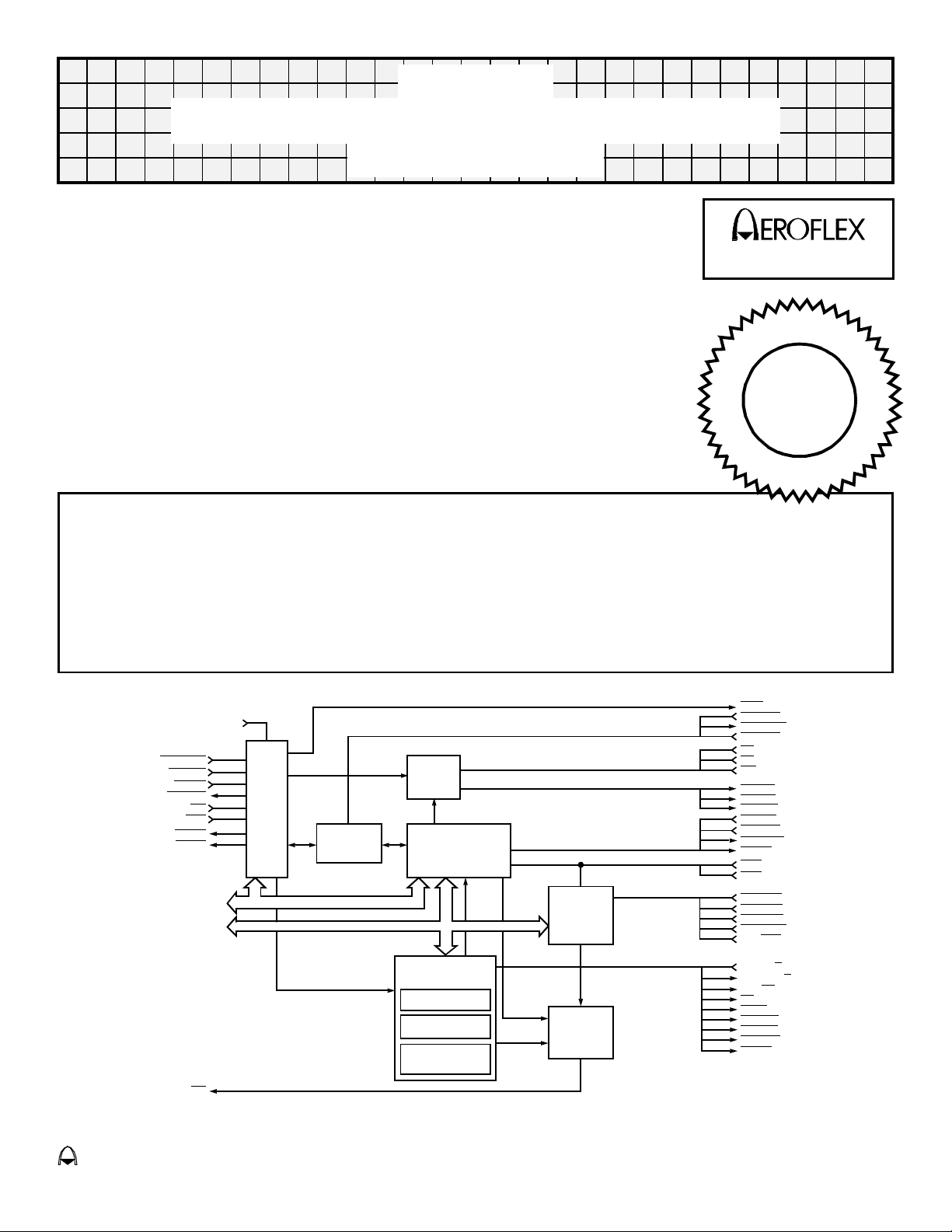
MIL-STD-1553 to Microprocessor
Interface Unit
Features
• Second Source Compatible to the BUS-66300
• PGA Version available, (second source to the BUS-66312)
• Compatible with MIL-STD-1750 CPUs
• Compatible with MOTOROLA, INTEL, and ZILOG CPUs
• Compatible with Aeroflex’s CT2565 BC/RT/MT and CT2512 RT
• Minimizes CPU overhead
• Signal controls for shared memory implementation
• Transfers complete messages to shared memory
• Provides memory mapped 1553 interface
• Packaging – Hermetic Metal
• 78 Pin, 2.1" x 1.87" x .25" PGA type package
• 82 Lead, 2.2" x 1.61 x .18" Flat Package
Description
Aeroflex CT2566 MIL-STD-1553 to Microprocessor Interface Unit simplifies the CPU to 1553 Data
Bus interface. The CT2566 provides an interface by using RAM allowing the CPU to transmit or
receive 1553 traffic simply by accessing the memory. All 1553 message transfers are entirely
memory or I/O mapped. The CT2566 supports 1553 interface devices such as Aeroflex's CT2512
dual RT or the CT2565 dual BC, RT, and MT. The CT2566 operates over the full military -55°C to
+125°C temperature range.
CIRCUIT TECHNOLOGY
ISO
9001
I
MSTRCLR
SELECT
STRBD
READYD
RD/
WR
MEM/
REG
EXTEN
EXTLD
INT
CLOCK IN
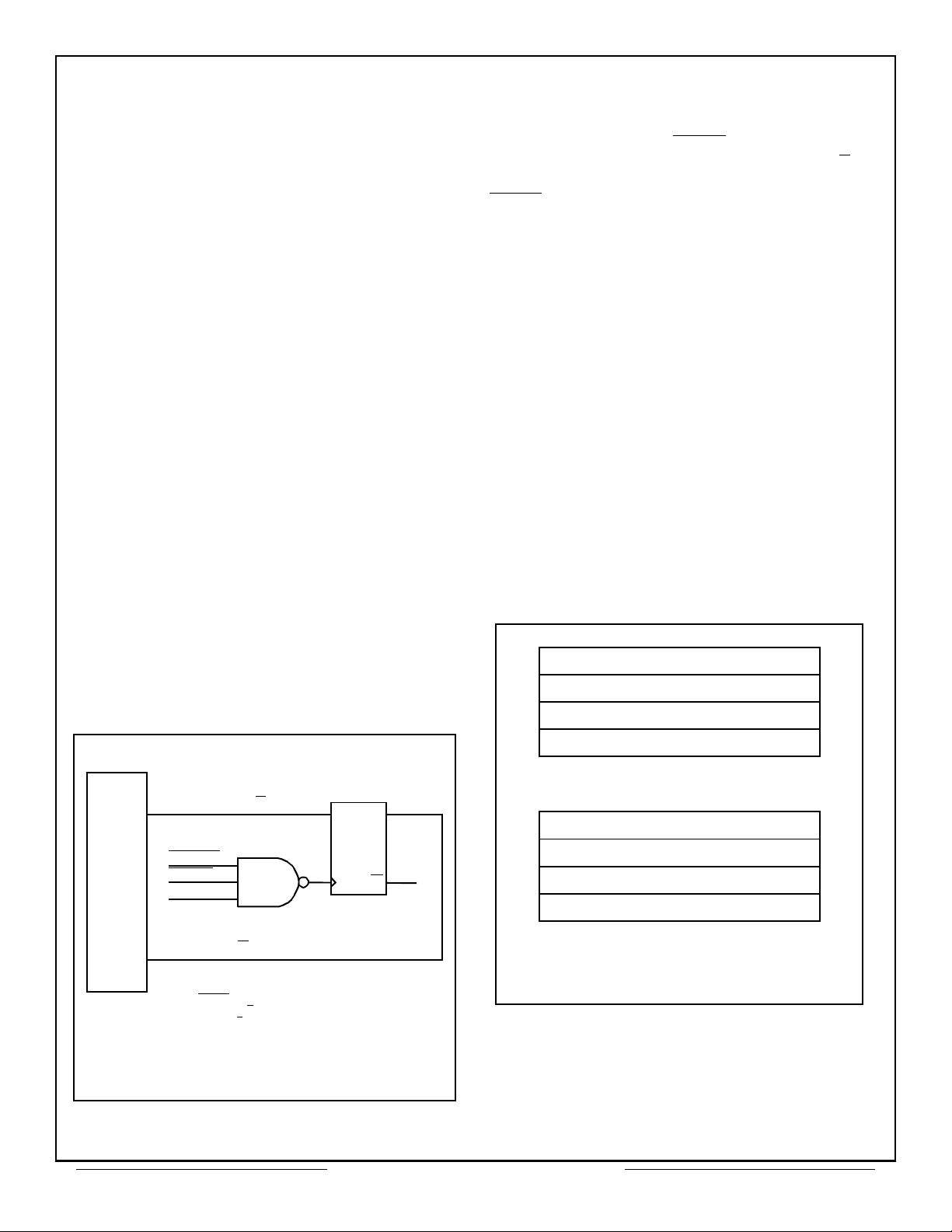
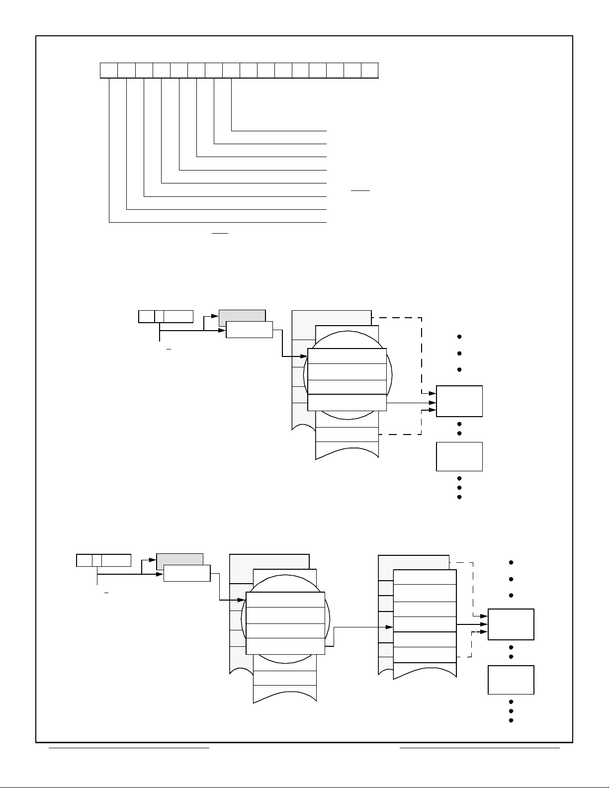
MEMORY
CPU
TIMING
A15-A00
D15-D00
CONTENTION
RESOLVER
TIMING
MICROCODE
CONTROLLER
OPERATION
CONTROL
REGISTERS
CONFIGURATION
REGISTER
START / RESET
REGISTER
INTERRUPT
MASK
REGISTER
Figure 1 – Functional Block Diagram
BLOCK
STATUS
WORD
INTERRUPT
GENERATOR
IOEN
BUSREQ
BUSGRNT
BUSACK
CS
OE
WR
MEMCS
MEMOE
MEMWR
ADRINC
NBGRNT
BCSTART
TAGEN
EOM
SOM
MSGERR
TIMEOUT
STATERR
LOOPERR
CHB/
CHA
CTLINB/
CTLOUTB/
RTU/
BC
MT
DBAC
SSBUSY
SSFLAG
SVCREQ
RESET
A
A
eroflex Circuit Technology – Data Bus Modules For The Future © SCDCT2566 REV B 8/10/99
Page 2
Specifications at Nominal Power Supply Voltages
PARAMETER VALUE UNITS
Logic
I
(With VIH = 2.7V)
IH
(With VIL = 0.0V)
I
IL
I
OH
I
OL
V
IH
V
IL
V
OH
V
OL
−630 µA
−700 µA
4.0 min mA
4.0 mA
2.0 V
0.8 V
3.7 V
0.4 V
Clock 12 MHz
Power Supplies
Voltage
Current Drain
5.0±10% V
10 typ mA
Temperature Range
Operating (Case)
Storage
−55 to +125 °C
−65 to +150 °C
Physical Characteristics
Size
78 pin DIP
82 pin flatpack
2.1 x 1.87 x 0.25
(53 x 47.5 x 6.4)
2.1 x 1.87 x 0.25
(55.6 x 40.6 x 3.71)
in
(mm)
in
(mm)
Weight
78 pin DIP
82 pin flatpack
1 (28) oz (g)
1 (28) oz (g)
Table 1 – Specifications
GENERAL
The CT2566 was designed to perform required
handshaking to the 1553 interface device, storing
or retrieving message(s) from a user supplied
RAM and notifying the CPU that a 1553
transaction has occurred. The CPU uses this
RAM to read the received data as well as to store
messages to be transmitted onto the Bus.
The CT2566 can be used to implement BC, RT,
or MT operation and can be either memory
mapped or I/O mapped to CPU address space.
Registers internal to the CT2566 control its
operation.
The CT2566 can access up to four external,
user supplied registers and can address up to
64K words of RAM. The RAM selected must be a
non-latched static RAM (capable of meeting the
timing constraints for the CT2566). A double
Aeroflex Circuit Technology SCDCT2566 REV B 8/10/99 Plainview NY (516) 694-6700
buffering architecture is provided to prevent
incomplete or partially updated information from
being transmitted onto the 1553 Data Bus.
The CT2566 requires an external, user supplied
clock.
COMPATIBLE MICROPROCESSOR TYPES
The CT2566 may be used with most common
microprocessors, including, the Motorola 68000
family, the Intel 8080 family, Zilog Z8000
products, and available MIL-STD-1750
processors.
Interfacing the CT2566 to the 1553 Data Bus
requires external circuitry such as Aeroflex’s
CT2565(BC/RT/MT) and ACT4489D
transceivers. Figure 2 shows the interconnection
for these components.
2
Page 3
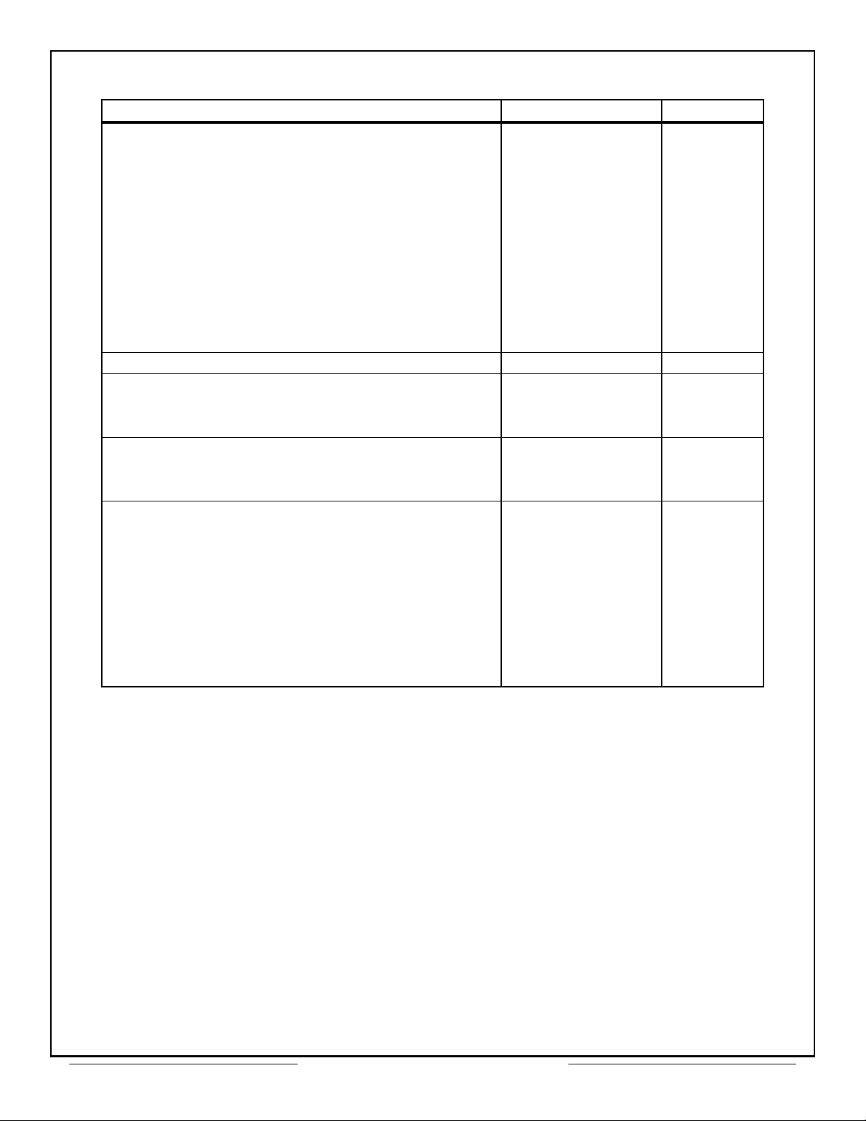
PIN NO. NAME I/O DESCRIPTION
1 SELECT
2 RD/WR
3 READYD
I
I
O
Select. When active, selects CT2566 for operation.
Read/Write. Controls CPU bus data direction.
Ready Data. When active indicates data has been received
from, or is available to the CPU.
4 EXTEN
O
External Enable. Output from CT2566 to enable output from
external devices. Same timing as MEMOE
5 TAGEN
O
Tag Enable. Enables an external time tag counter for
transferring the time tag word into memory.
6 EOM
I
End of Message. Input from 1553 device indicating end of
message.
7 SOM
I
Start of Message. Input from 1553 device indicating start of
message in RTU mode.
8 STATERR
I
Status Error. Input from 1553 device when status word has
either a bit set or unexpected RT address (in BC mode only).
9 ADRINC
I
Address Increment. Sent from 1553 device to increment
address counter following word transfer.
10 MEM/REG
I
Memory/Register. Input from CPU to select memory or
register data transfer.
11 CLOCK IN I
12 LOOPERR
13 BUSREQ
I
I
Clock input; 50% duty cycle, 12MHz, max.
Loop Error. Input from 1553 device if short loop BIT fails.
Bus Request. When active, indicates 1553 device requires
use of the address/data bus.
14 BUSGRNT
O
Bus Grant. Handshake output to 1553 device in response to
BUS REQUEST indicating address/data bus available to
1553 device.
15 Not Used -
16 MEMCS
O
-
Memory Chip Select. Low from CT2566 to enable external
RAM. Used with 4K x 4 RAM type device to read RAM or
used in conjunction with MEMWR
17 OE
I
Output Enable. Input from 1553 device used to enable
memory on the parallel bus.
18 N/C -
19 NBGRNT
I
Not Used.
Low pulse from 1553 device preceding start of received new
protocol sequence. Used with superseding command to reset
DMA in progress.
20 + 5 Volt I
21 D15 I/O
22 D13 I/O
23 D11 I/O
24 D09 I/O
25 D07 I/O
26 D05 I/O
Logic power supply.
Data Bus Bit 15 (MSB).
Data Bus Bit 13.
Data Bus Bit 11.
Data Bus Bit 9.
Data Bus Bit 7.
Data Bus Bit 5.
27 D03 I/O Data Bus Bit 3.
.
to write data into RAM.
Table 2 – Pin Functions (78 Pin DIP)
Aeroflex Circuit Technology SCDCT2566 REV B 8/10/99 Plainview NY (516) 694-6700
3
Page 4
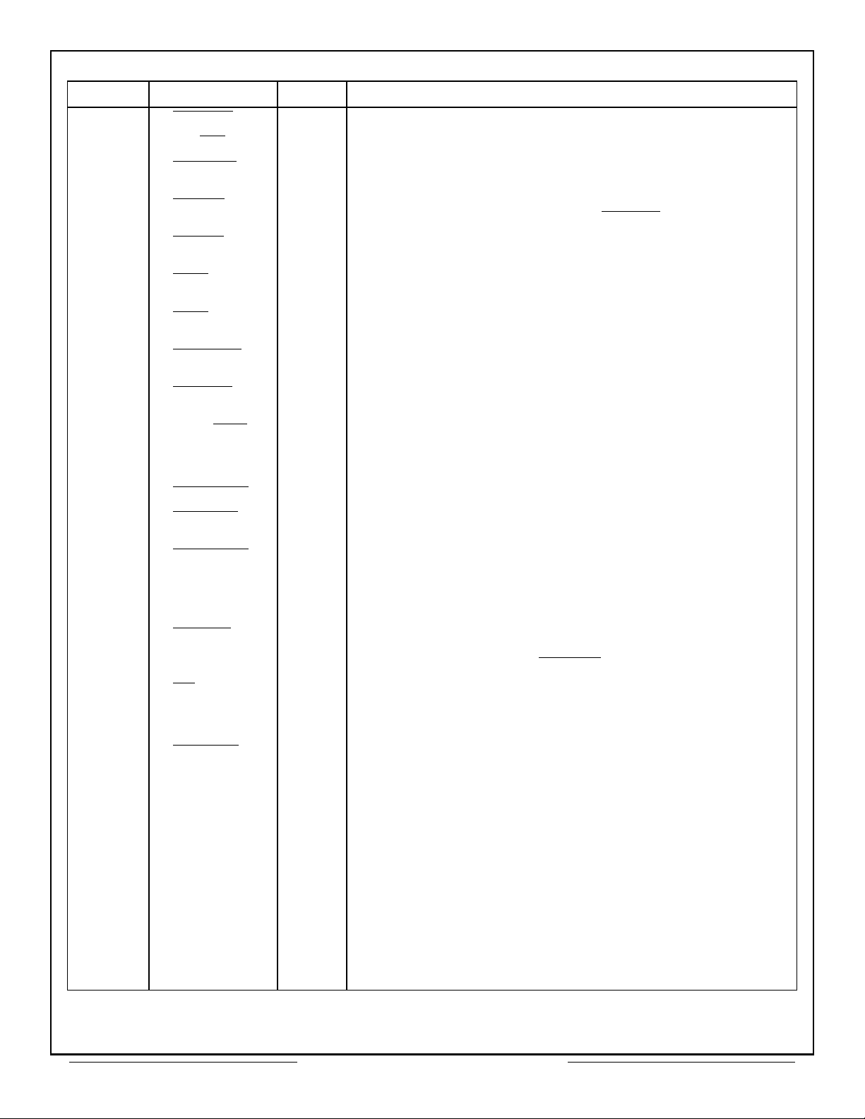
PIN NO. NAME I/O DESCRIPTION
28 D01 I/O Data Bus Bit 1.
29 SSFLAG
O
Subsystem Flag. Output to 1553 device to set RT subsystem
flag status bit.
30 SSBUSY
O
Subsystem Busy. Output to 1553 device to set RT subsystem
busy flag.
31 RTU/BC
O
Output to 1553 device used in conjunction with MT to set
operating mode.
32 A14 O Address Bit 14.
33 A12 O Address Bit 12.
34 A10 O Address Bit 10.
35 A08 O Address Bit 8.
36 A06 O Address Bit 6.
37 A04 O Address Bit 4.
38 A02 I/O Address Bit 2.
39 A00 I/O Address Bit 0 (LSB).
40 GND - Signal Return.
41 STRBD
I
Strobe Data. Used in conjunction with SELECT
data transfer cycle to/from CPU.
42 IOEN
O
Input/Output Enable. Output from CT2566 to enable external
buffers/latches connecting the hybrid to the address/data
bus.
43 EXTLD
O
External Load. Used to load data into external device via the
CT2566 data bus. Same timing as MEMWR
44 CHB/CHA
Input from 1553 in RT mode used to indicate received 1553
message came in either Channel A or B.
to indicate a
.
45 INT
46 BCSTART
47 RESET
48 MSGERR I
49 CTLIN B/A
50 CTLOUT B/A
51 TIMEOUT
52 MSTRCLR
53 BUSACK
54 WR
55 CS
Table 2 – Pin Functions (78 Pin DIP) (Cont.)
O Interrupt. Interrupt pulse line to CPU.
O Bus Controller Start. Outputs to 1553 in initiate BC cycle.
O
Reset. Output to external device from CT2566 consisting of
the OR condition of CPU reset and CPU Master Clear.
Message Error. Input from 1553 device when an error occurs
in message sequence.
I Input to change active memory map area (0 = area A).
O
Output from CT2566 selecting which area is to be active (0 =
area A).
I Input from 1553 device indicating no response time-out.
I
Master Clear. Power-on reset from CPU. Resets DMA in
progress and internal registers to logic “0”.
I
Bus Acknowledge. Input from 1553 device acknowledge
receipt of BUSGRNT
.
I Write. Input from 1553 device for writing data into memory.
I
Chip Select. Input from 1553 device that is routed to
MEMCS
.
Aeroflex Circuit Technology SCDCT2566 REV B 8/10/99 Plainview NY (516) 694-6700
4
Page 5
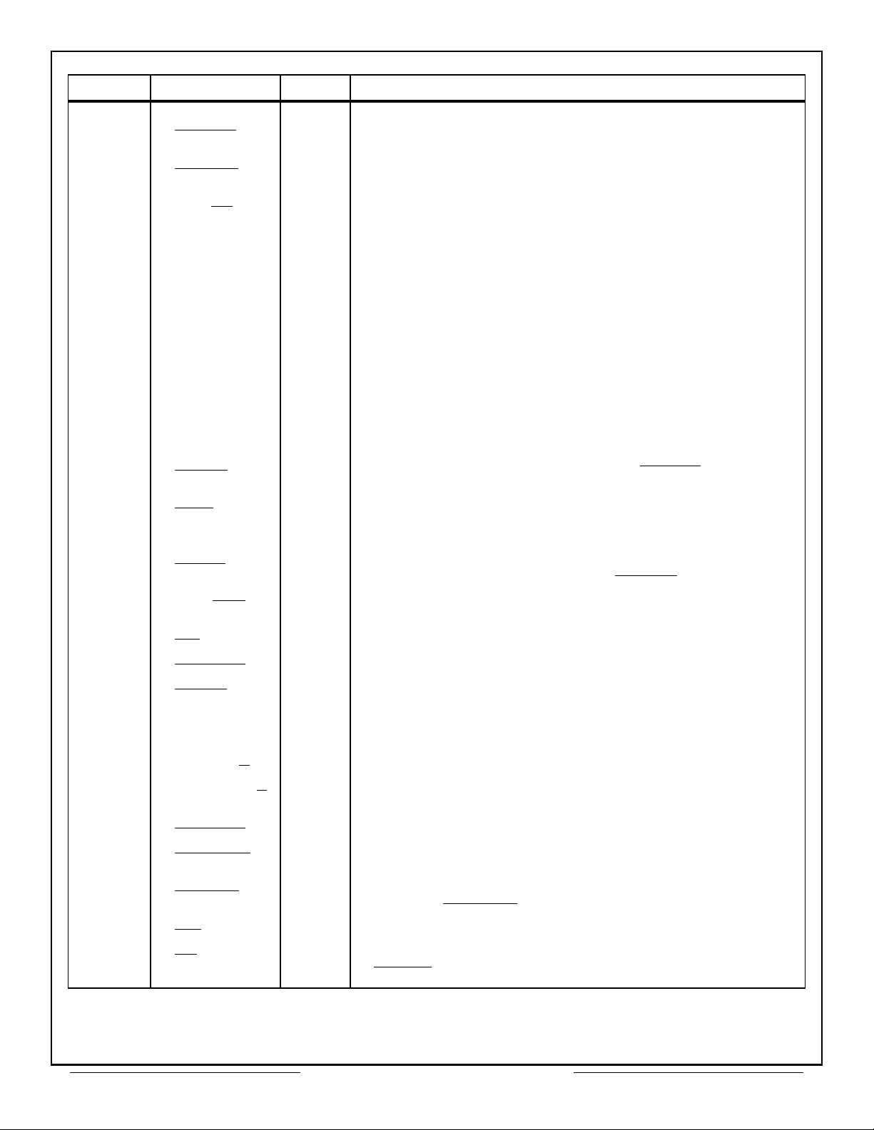
PIN NO. NAME I/O DESCRIPTION
56
MEMOE
O Memory Output Enable. Output from CT2566 to enable
memory output data.
57 MEMWR O
Memory Write. Output pulse from CT2566 to write data bus
data into memory.
58 Not Used - -
59 MT
O
Bus Monitor. Used in conjunction with RTU/BC
operating mode.
60 D14 I/O Data Bus Bit 14.
61 D12 I/O Data Bus Bit 12.
62 D10 I/O Data Bus Bit 10.
63 D08 I/O Data Bus Bit 8.
64 D06 I/O Data Bus Bit 6.
65 D04 I/O Data Bus Bit 4.
66 D02 I/O Data Bus Bit 2.
67 D00 I/O Data Bus Bit 0 (LSB).
68 SVCREQ
O
Service Request. Used to set service request bit in RT Status
Word.
69 DBAC
O
Dynamic Bus Acceptance. Used to set status bit in RT Status
Word.
to set
70 A15 O Address Bit 15 (MSB).
71 A13 O Address Bit 13.
72 A11 O Address Bit 11.
73 A09 O Address Bit 9.
74 A07 O Address Bit 7.
75 A05 O Address Bit 5.
76 A03 O Address Bit 3.
77 A01 I/O Address Bit 1.
78 GND - Chassis Ground.
Table 2 – Pin Functions (78 Pin DIP) (Cont.)
PIN NO. FUNCTION PIN NO. FUNCTION
1 N/C 42 N/C
2 SELECT
3 STRBD
4 RD/WR
5 IOENBL
43 GROUND
44 CHASSIS GROUND
45 A00 (LSB)
46 A01
6 READYD
7 EXTLD
47 A02
48 A03
Table 3 – CT2566FP Pin Functions (82 Pin Flat Package)
Aeroflex Circuit Technology SCDCT2566 REV B 8/10/99 Plainview NY (516) 694-6700
5
Page 6
PIN NO. FUNCTION PIN NO. FUNCTION
8 EXTEN 49 A04
9 CHB/CHA
10 TAGEN
11 INT
12 EOM
13 BCSTART
14 SOM
15 RESET
16 STATERR
17 MSGERR
18 ADRINC
19 CTLIN B/A
20 MEM/REG
50 A05
51 A06
52 A07
53 A08
54 A09
55 A10
56 A11
57 A12
58 A13
59 A14
60 A15
61 RTU/BC
21 CTLOUT B/A 62 DBAC
22 CLOCK IN 63 SSBUSY
23 TIMEOUT 64 SVCREQ
24 LOOPERR 65 SSFLAG
25 MSTRCLR 66 D00
26 BUSYREQ
27 BUSACK
28 BUSGRNT
29 WR
67 D01
68 D02
69 D03
70 D04
30 N/C 71 D05
31 CS
32 MEMCS
33 MEMOE
34 OE
35 MEMWR
72 D06
73 D07
74 D08
75 D09
76 D10
36 Not Used 77 D11
37 N/C 78 D12
38 NBGRNT
39 MT
79 D13
80 D14
40 +5V 81 D15
41 N/C 82 N/C
Table 3 – CT2566FP Pin Functions (82 Pin Flat Package) (Cont.)
Aeroflex Circuit Technology SCDCT2566 REV B 8/10/99 Plainview NY (516) 694-6700
6
Page 7
MEMORY MANAGEMENT
BUS-66300
Figure 3 – Synchronized map switching u
the CT2566
The RAM used by the CT2566 can be any standard
static memory with a WRITE STROBE pulse width
requirement less than 70ns. The RAM area is broken
down into pointers, look-up tables, and data blocks. All
1553 operation control is accomplished through the
RAM, including fault monitoring and data block
transfers.
For most applications, a 4K x 16 memory is sufficient
to store the number of messages, but the CT2566 can
access up to 64K words.
DOUBLE BUFFERING
A Double Buffering system is available to prevent
partially updated data blocks from being read by the
CPU or transferred onto the 1553 Data Bus. To use
Double Buffering the CPU must divide the RAM into
two areas: “current” and “non-current”. Two Stack
Pointers, Descriptor Stacks, and Look-Up Tables are
required to be used by the CPU.
The 1553 device has access only to the current area
of RAM, and will use the current Descriptor Stack and
Look-Up Table. While the 1553 device is processing
messages using the current area pointers, the CPU
can be setting up the next set of messages in the
non-current area of RAM.
Once an EOM or BCEOM occurs, the CPU can swap
the current and non-current areas by toggling bit 13 of
the Configuration Register (See register section for
description). The 1553 device will then have access to
the new current area. Meanwhile, the CPU can begin
processing the data received during the previous
transfer or can begin setting up the next set of 1553
messages.
to ensure that the swapping of the current and
non-current areas doesn’t occur while the CT2566 is
processing a message from the 1553 device. During
message processing, the INCMD
CPU’s map area selection is inhibited. CTLIN B/A
is a logic "0" and the
will
be automatically latched back into the CT2566 when
INCMD
and NODT change to a logic "1".
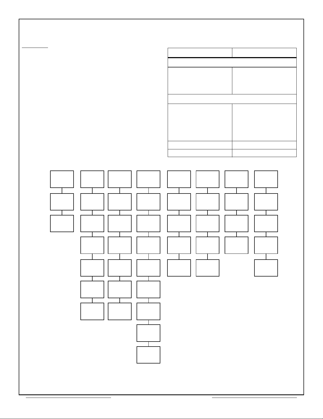
DESCRIPTOR STACK
The CT2566 uses a Descriptor Stack in BC and RTU
modes. Each stack entry contains four words which
refer to one 1553 message (See Figure 4). The Block
Status Word, shown in Figure 5, indicates the physical
bus which received the message (RTU mode), reports
whether or not an error was detected during message
transfer, and indicates whether the message was
completed (SOM replaced with EOM).
The user-supplied Time-Tag word is loaded at the
start of a message transfer and is updated at the end of
the transfer.
The contents of the fourth word in the Descriptor
Stack depends on the operating mode. In BC mode, it
contains the address of the message data block
containing the 1553 message formatted as shown in
Figure 6. In RTU mode, the word contains the received
1553 Command Word as shown in Figure 7.
A Stack Pointer must be initialized by the CPU. The
Descriptor Stack contains 64, four word entries, and
BLOCK STATUS WORD
TIME TAG WORD
RESERVED
MESSABE BLOCK ADDRESS
50 CTLOUT B/A
INCMD
NODT
12 MHz
49 CTLIN B/A
Notes:
(1) INCMD
(2) CTLOUT B/A
(3) CTLIN B/A
is from the BUS-65600 or BUS-65112.
reflects bit 13 of the Configuration Register.
is used to select the current area.
D Q
LS74
C
Q
An external circuit (shown in Figure 3) can be added
Aeroflex Circuit Technology SCDCT2566 REV B 8/10/99 Plainview NY (516) 694-6700
BC DESCRIPTION BLOCK
BLOCK STATUS WORD
TIME TAG WORD
RESERVED
RECEIVED COMMAND WORD
RTU DESCRIPTION BLOCK
Figure 4 – Descriptor Stack Entries
automatically wraps around (the 64th entry is followed
by the first entry). The 1553 device uses the current
area Stack Pointer to determine the address of the
Stack entry to be used for the current 1553 message.
The CT2566 automatically increments the current area
Stack Pointer by four upon the completion of each
7
Page 8
message regardless of whether or not an error was
External Register
detected during the processing of that message.
LOOK-UP TABLES
In RTU mode a Look-Up Table is provided to allow
the CT2566 to store messages in distinct areas of RAM
based upon the subaddress of the received command
word. See RTU operation for details.
The CT2566 uses the T/R
bits to form a pointer into the “current area” Look-Up
Table. The first 32 words of this table are initialized by
the user with the addresses of the data blocks to be
used for receiving data into subaddress 0,1,2,…31.
The next 32 words are initialized by the user with the
address of the data blocks to be used when
transmitting data from subaddress 0,1,2,…31.
and the five subaddress
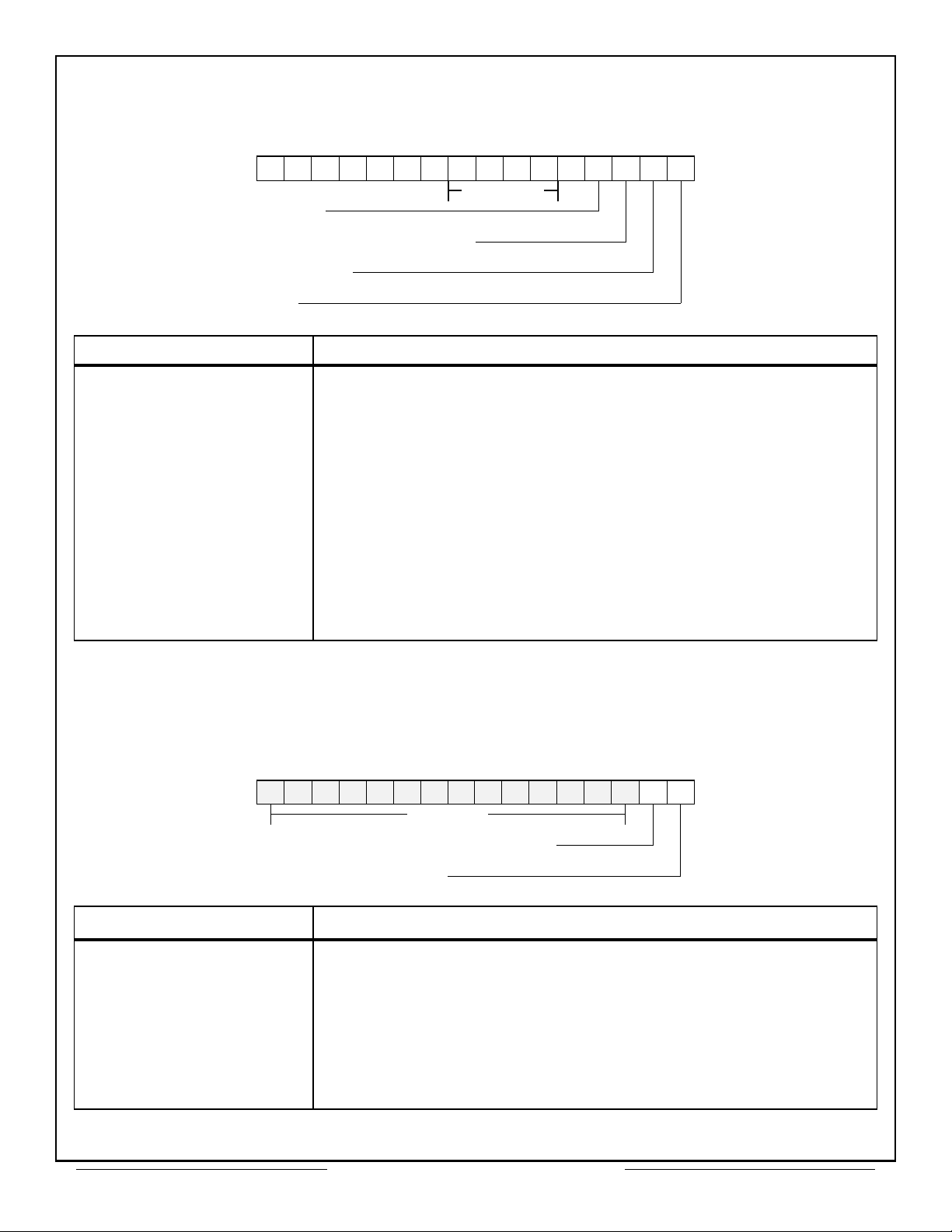
CT2566 REGISTERS
The CT2566 is controlled through the use of three
internal registers: the Interrupt Mask Register,
Configuration Register, and Start/Reset Register. In
15 14 13 12 11 10 9 8 7 6 5 4 3 2 1 0
1 1 1 1 1 1 1 1
addition, the CT2566 can access up to four external,
user supplied registers. Possible external register
applications include: defining the RTU address, storing
a CPU Time Tag, and reading a captured Built-In-Test
(BIT) Word from the 1553 interface unit. For further
information, consult factory.
Table 2 – Internal Registers Address Definition
CT2566
Address Bits
Definition
A2 A1 A0
0 0 0 Interrupt Mask Register
0 0 1
0 1 0
0 1 1
1 0 0
1 0 1
1 1 0
Configuration Register
Not Used
Start/Reset Register (write
only)
External Register
External Register
External Register
1 1 1
SUBSYSTEM FLAG
SERVICE REQUEST
BUSY
DB ACCEPT
STOP ON ERROR
CONTROL AREA BIT B/A
MT
RTU/BC
BIT DEFINITIONS
SUBSYSTEM FLAG
SERVICE REQUEST
BUSY
DB ACCEPT
1553 status word bit.
1553 status word bit.
1553 status word bit.
1553 status word bit.
STOP ON ERROR Causes BC to stop at the end of current data block if an error is detected.
CONTROL AREA B/A
RTU/BC
/MT Operating Mode.
Used for double buffering (See Double Buffering).
Bit 15 Bit 14
Mode
0 0 BC
0 1
1 0
1 1
MT
RTU
ILLEGAL
Figure 8 – Configuration Register
Aeroflex Circuit Technology SCDCT2566 REV B 8/10/99 Plainview NY (516) 694-6700
8
Page 9
15 14 13 12 11 10 9 8 7 6 5 4 3 2 1 0
1 1 1 1 1 1 1 1
LOOP TEST FAIL
RESPONSE TIME OUT (BC ONLY)
FORMAT ERROR
STATUS SET (BC ONLY)
ERROR FLAG
CHB/CHA
(RTU ONLY)
SOM
EOM
Note: In BC mode Bit 13, CHB/CHA contains a logic "0" regardless of which channel is used.
Figure 5 – Block Status Word
CONFIGURATION
REGISTER
CONFIGURATION
REGISTER
CURRENT
AREA B/
A
01315
STACK
POINTERS
Note: User may opt to share memory block(s).
Figure 6 – Use of Descriptor Stack – BC Mode
STACK
POINTERS
01315
DESCRIPTOR
STACKS
DESCRIPTOR
STACKS
BLOCK STATUS WORD
TIME TAG WORD
RESERVED
MESSAGE
BLOCK ADDR
LOOK-UP TABLE
(DATA BLOCK ADDR)
DATA
BLOCKS
DATA BLOCK
DATA BLOCK
DATA
BLOCKS
(1)
CURRENT
AREA B/
A
Note: (1) User may opt to share memory block(s).
(2) See Figure 19.
BLOCK STATUS WORD
TIME TAG WORD
RESERVED
RECEIVED COMMAND
WORD
LOOK-UP
TABLE ADDR
(2)
DATA BLOCK
DATA BLOCK
Figure 7 – Use of Descriptor Stack – RTU Mode
Aeroflex Circuit Technology SCDCT2566 REV B 8/10/99 Plainview NY (516) 694-6700
9
Page 10
INTERRUPT MASK REGISTER
This register is an eight bit read/write register used to enable the interrupt conditions. All interrupts are enabled
with a logic "1" (See Figure 9).
15 4 3 2 1 0
1 1 1 1 1 1 1
NOT USED
BC EOM
FORMAT ERROR/STATUS SET
NOT USED
EOM
INTERRUPT DEFINITION
EOM End of Message. Set by CT2566 (during BC or RTU mode) every time a
1553 message is transferred (regardless of validity).
FORMAT ERROR/
STATUS SET
Set by CT2566 for these conditions:
Loop Test Failure: Last transmitted word did not match received word.
Message Error: Received message contained an address error, one of
eight 1553 status bits set, or 1553 specification violated (parity error,
Manchester error, etc).
Time-Out: Expected transmission was not received during allotted time
Status Set: Received status word contained status bit(s) set or address
error.
BC EOM
Bus Controller End of Message. Set by CT2566 (in BC mode) when all
messages have been transferred.
Figure 9 – Interrupt Mask Register
START/RESET REGISTER
Only two bits of this write only register are used, as illustrated in Figure 10.
15 1 0
NOT USED
CONTROLLER START
RESET
BIT DEFINITION
RESET Issued by the CPU to place the CT2566 in the power-on condition;
Configuration, and Interrupt Mask registers are reset to logic “0”.
CONTROLLER START
Issued by the CPU (BC mode) to start message transmission. The CPU
must first load the number of messages to transfer (256, max) in the
message count location of RAM (area A or B). Value is loaded in 1’s
complement (load FFFE to transmit one message). In MT mode it is
used to begin reception of 1553 messages. Issued by CPU in MT mode
to enable monitor operation.
Figure 10 – Start/Reset Register
Aeroflex Circuit Technology SCDCT2566 REV B 8/10/99 Plainview NY (516) 694-6700
10
Page 11
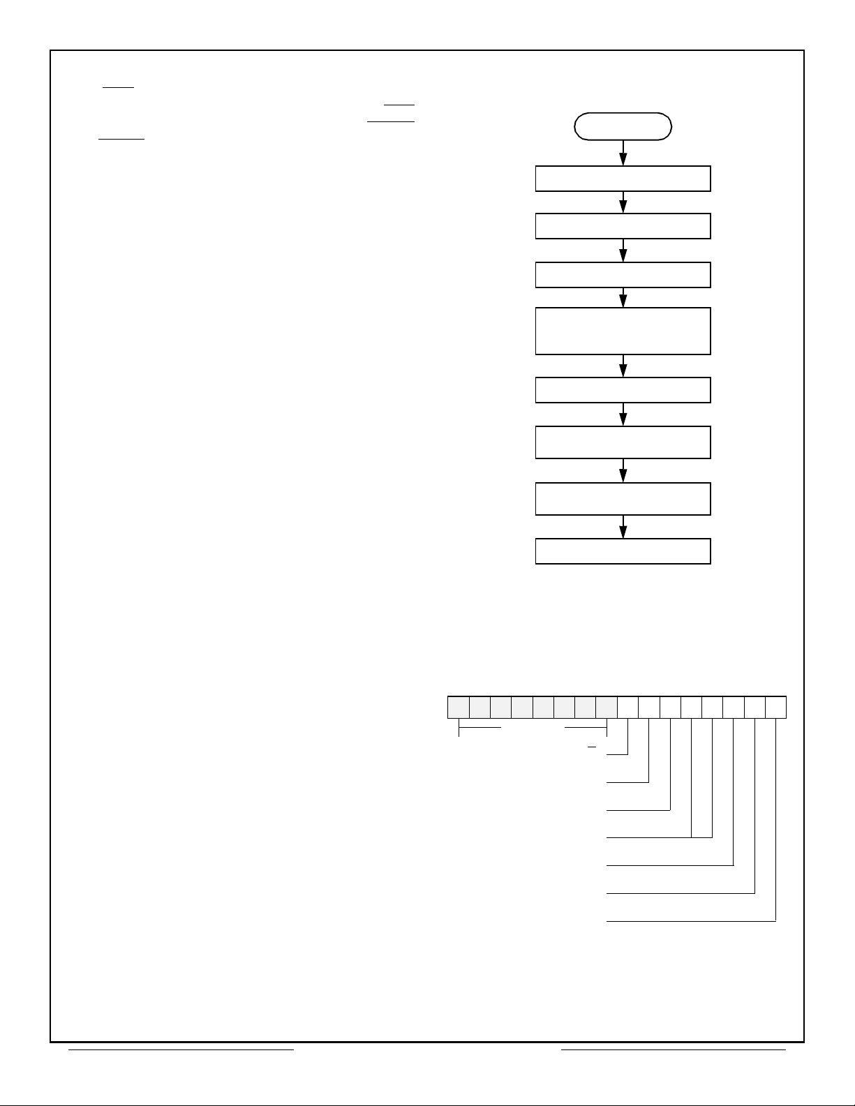
BC Operation
The BC mode is selected by setting the two MSBs of
the Configuration Register to logic "0". This can be done
by writing directly to the register or by issuing a
MSTRCLR
will also clear the Interrupt Mask Register.
BC Initialization.
For BC operation, the user initializes the RAM as
shown in Table 3 and follows the steps in Figure 11, BC
Initialization. The CPU loads the data blocks with 1553
messages (See Figure 12). The first word of each data
block must contain the Control Word (shown in Figure
13) for the message. The starting addresses of the data
blocks are placed in the fourth word of the Descriptor
Stack in the order the messages are to be transmitted
(i.e. the address of the first message is loaded into the
fourth location of the Stack, the address of the second
message is placed into the eighth location, etc). Once
the data blocks and the Descriptor Stack have been
initialized, the CPU loads the current area message
count with the number of messages to transfer (load in
1’s complement).
or RESET command. Note that a RESET
Table 3 - Typical BC Memory Map
(4K memory)]
HEX ADDRESS FUNCTION
Fixed Areas
0100 Stack Pointer A
0101 Message Count A
0104 Stack Pointer B
0105 Message Count B
User Defined Areas
0108-013F Not Used
0140-017F Data Block 1
0180-01BF Data Block 2
01C0-01FF Data Block 3
• •
• •
0F00-0FFF Descriptor Stack A
0000-00FF Descriptor Stack B
CONTROL
WORD
BROADCAST
COMMAND
(NO DATA)
BROADCAST
COMMAND
LOOPED
BACK BY
CT2565
BROADCAST
COMMAND
(NO DATA)
CONTROL
WORD
RECEIVE
COMMAND
DATA WORD
1
DATA WORD
2
DATA WORD
LAST
DATA WORD
LAST
LOOPED
BACK BY
CT2566
STATUS
RECEIVE
RECEIVE
DATA BLOCK
CONTROL
WORD
TRANSMIT
COMMAND
TRANSMIT
COMMAND
LOOPED
BACK BY
CT2565
STATUS
RECEIVED
DATA WORD
1
DATA WORD
2
DATA WORD
LAST
TRANSMIT
DATA BLOCK
CONTROL
WORD
RECEIVE
COMMAND
TRANSMIT
COMMAND
TRANSMIT
COMMAND
LOOPED
BACK BY
CT2565
STATUS
WORD 1
FROM XMTR
DATA WORD
1 RECEIVED
DATA WORD
2 RECEIVED
LAST DATA
WORD
RECEIVED
CONTROL
WORD
MODE
COMMAND
DATA WORD
DATA WORD
LOOPED
BACK BY
CT2565
STATUS
WORD
MODE CODE
WITH DATA
RECEIVE
DATA BLOCK
FORMAT
CONTROL
WORD
MODE
COMMAND
MODE
COMMAND
LOOPED
BACK BY
CT2565
STATUS
WORD
DATA WORD
RECEIVED
MODE CODE
WITH DATA
TRANSMIT
DATA BLOCK
FORMAT
CONTROL
WORD
MODE
COMMAND
MODE
COMMAND
LOOPED
BACK BY
CT2565
STATUS
WORD
MODE CODE
WITHOUT
DATA
BROADCAST
COMMAND
DATA WORD
1
DATA WORD
2
DATA WORD
LAST
DATA WORD
LOOPED
BACK BY
CT2565
BROADCAST
COMMAND
WITH DATA
STATUS
WORD 2
FROM
RECEIVER
REMOTE
TERMINAL TO
REMOTE
TERMINAL
DATA BLOCK
Figure 12 – BC Message Data Block Formats
Aeroflex Circuit Technology SCDCT2566 REV B 8/10/99 Plainview NY (516) 694-6700
11
Page 12
The CPU selects an internal register by asserting
Figure 13 – BC Control Word
MEM/REG
and the A2 bit to logic "0" (See Table 2).
External registers are selected by asserting MEM/REG
logic "0" and A2 bit to a logic "1". The signals EXTEN
and EXTLD are used to read and write from the
external registers (See Figures 26 to 28).
Configuration Register
The Configuration Register is an eight bit read/write
register used to define the 1553 operating mode (BC,
MT, or RTU) and the associated RTU status bits. The
four MSBs define the mode of operation; the four LSBs
define the RTU status bits (See Figure 8).
All bits in the Configuration Register (except bit 12)
will be present on the respective CT2566 output pins to
the 1553 device. The MT bit is inverted at the output.
To begin transferring messages onto the bus, the
CPU must issue a Controller Start Command (See
Figure 14). This is done by setting bit 1 of the
Start/Reset Register to a logic "1". An EOM interrupt
will be generated each time a message transfer has
been completed. A BCEOM will be generated once the
specified number of messages has been transferred
(message counter = FFFF).
A Format Error Status Set Interrupt will be generated
at the end of a message if a timeout condition or error
condition was detected. If the STOP ON ERROR bit in
the Configuration Register is set, the CT2566 will stop
bus transactions until a new Controller Start command
is issued by the CPU. These interrupts may be masked
by the CPU through the Interrupt Mask Register.
1. Reads the Stack Pointer to get the address of the
current Descriptor Stack Entry.
START
ISSUE RESET COMMAND
INITIALIZE STACK POINTER
LOAD MESSAGE COUNTER
LOAD EVERY FOURTH
LOCATION OF STACK WITH
STARTING ADDRESS
LOAD MESSAGES
SET CONFIGURATION
RESISTER TO BC MODE
INITIALIZE INTERRUPT
MASK REGISTER
ISSUE START COMMAND
Figure 11
BC Initialization (under user control)
BC START SEQUENCE
After setting the CONTROLLER START bit in the
Start/Reset Register, the CT2566 takes the following
actions:
1. Reads the Stack Pointer to get the address of the
current Descriptor Stack Entry.
2. Stores an SOM flag in the Block Status Word to
indicate a transfer operation is in progress.
3. Stores the Time Tag if used.
4. Reads the Data Block Address from the fourth
location of the Descriptor Stack and transfers the
Data Block Address into an internal Address
Register.
5. Issues a BCSTART pulse to the associated 1553
device to start the message transfers.
Note that data words are transferred to an from
memory by the associated 1553 interface unit using the
internal Address Register.
BC EOM Sequence.
Upon completion of a 1553 message (valid or invalid)
the 1553 interface unit issues an EOM pulse to the
CT2566 which takes the following actions:
15 8 7 0
NOT USED
BUS CHANNEL A/B
NOT USED
MASK BROADCAST BIT
NOT USED
MODE CODE
BROADCAST
RTU TO RTU
Note: When the BC expects the BROADCAST bit set in the status
word, a logic "1" will mask the status interrupt error flag. A
FORMAT error will be generated if the MASK BROADCAST bit
is not set.
Aeroflex Circuit Technology SCDCT2566 REV B 8/10/99 Plainview NY (516) 694-6700
12
Page 13

CONTROLLER START
*
COMMAND RECEIVED
READS STACK POINTER
LOAD BLOCK STATUS WORD
INTO FIRST WORD OF
DESCRIPTOR STACK ENTRY
(SET SOM BIT IN BLOCK
STATUS WORD)
LOAD TIME TAG INTO
SECOND WORD OF
DESCRIPTOR
STACK ENTRY
OBTAIN DATA BLOCK
ADDRESS FROM FOURTH WORD
ISSUE BC START TO 1553 DEVICE
READ CONTROL WORD TO
DETERMINE TYPE OF TRANSFER
TRANSFER DATA TO/FROM
1553 BUS (NOTE: RAM NOW
CONTROLLED BY INPUT PINS
UPDATE BLOCK STATUS WORD
AND OE
CS
UPDATE TIME TAG
INCREMENT STACK
POINTER BY FOUR.
DECREMENT
MESSAGE COUNT
DATA BLOCK
TRANSFERRED OK
TRANSFERRED OK
?
NO
STOP ON
ERROR SET
?
YES
YES
NO
MORE MESSAGES
TO SEND
?
NO
ISSUE BC EOM
STOP
YES
After controller start is issued the subsystem must wait until BCEOM is active
*
before issuing the next controller start.
Figure 14 – BC Sequence of Operation (Under CT2566 Control)
Aeroflex Circuit Technology SCDCT2566 REV B 8/10/99 Plainview NY (516) 694-6700
13
Page 14

2. Updates the Block Status Word by resetting the
RTU LOOK-UP TABLE ADDRESS
SOM and setting EOM and any error bits.
3. Updates the Time Tag if used.
4. Increments the contents of the Stack Pointer by
four and increments the Message Counter by
one.
5. Initiates a message transfer beginning with new
Controller Start sequence if more messages are
to be transmitted.
6. Generates a BCEOM interrupt if enabled and no
further messages are to be transmitted.
Note that if an error is received and STOP ON
ERROR is set, the CT2566 completes the current
BCEOM sequence and then stops. The Stack Pointer
will point to the next message to be transmitted.
Table 4 – Typical RTU memory map (4K memory)
HEX ADDRESS FUNCTION
Fixed Areas
0100 Descriptor Stack Pointer A
0101 Reserved
0104 Descriptor Stack Pointer B
0105 Reserved
0108-013F Spare
0140-017F Look-Up Table A
01C0-01FF Look-Up Table B
User Defined Areas
RTU Operation
The RTU mode is selected by setting bit 15 of the
Configuration Register to logic "1" and bit 14 to
logic"0".
RTU Initialization
For RTU operation, the user initializes the RAM as
shown in Table 4 and follows the steps shown in Figure
15, RTU Initialization Chart.
Look-Up Tables
The first 32 words of the Look-Up Table are initialized
with the addresses of the data blocks to be used when
received data from subaddress 0, 1, 2,…31. The next
32 table locations should be initialized with the address
of the data blocks to be used when the RTU is
instructed to transmit data from subaddress 0, 1,
2,…31. The data blocks may be any length sufficient to
contain the particular message as long as the data
block does not cross a 256 word boundary. Data blocks
may be shared by Look-Up Tables A and B, if desired
by the user (See Figure 16). The 1553 device can only
access the current Look-Up Table and the current
Descriptor Stack. The CPU selects the current area
through bit 13 of the Configuration Register.
Once in the RTU mode, the CT2566 will store the
command word in the fourth location of the current area
Descriptor Stack. The status of the message will be
recorded in the first location of the stack.
The data associated with the message will be
transferred to/from the data block indicated by the
Look-Up Table entry for that subaddress. If a system
Time Tag is provided by the user the CT2566 will
record the time of the SOM sequence in the second
word of the Stack entry.
When the CT2566 received an EOM pulse from the
1553 device, it resets the SOM bit in the Block Status
Word and sets the EOM bit and any error bits as
necessary. The Time Tag entry will be updated and an
EOM interrupt will be generated by the CPU, if enabled.
0180-019F Data Block 1
01A0-01BF Data Block 2
0200-021F Data Block 3
0220-023F Data Block 4
0240-025F Data Block 5
0260-027F Data Block 6
• •
• •
0EE0-0EFF Data Block 107
0000-00FF Descriptor Stack A
0F00-0FFF Descriptor Stack B
15 8 7 6 5 4 0
0 0 0 0 0 0 0 0 1
CURRENT AREA B/A
(CONFIG. REG BIT 13)
TR (FROM COMMAND
WORD)
RTU SUBADDRESS BITS
(FROM COMMAND WORD)
RTU SOM Sequence
Initiated when 1553 terminal puts a 1553 command
word on D00-D15 and pulses SOM
saves the command received in an internal register.
Figure 17 illustrates the RTU Sequence of Operation
once a 1553 command word is received. Once the
command word is received, the CT2566 performs the
following steps:
1. Reads the Stack Pointer to get the address of the
current Descriptor Stack Entry.
2. Stores a SOM flag in the Block Status Word to
indicate a transfer operation is in progress.
3. Stores the Time Tag if used.
low. The CT2566
Aeroflex Circuit Technology SCDCT2566 REV B 8/10/99 Plainview NY (516) 694-6700
14
Page 15

4. Stores the Command Word received.
(under CT2566 control)
}
Figure 16 – RTU Look-up Table
5. Reads a Block address from the Look-Up Table
using the T/R
bit and the subaddress from the
Command Word; transfers the Block address into
the address register. Data words are transferred
to/from memory by the associated 1553 interface
unit using the address register.
START
ISSUE RESET COMMAND
RTU EOM Sequence
At the end of a 1553 message (valid or invalid) the
CT2566 received an EOM pulse and then performs the
following:
1. Updates the Block Status Word.
2. Updates the Time Stage if used.
3. Increments the Stack Pointer by four.
4. Generates an Error Interrupt if enabled.
1553 COMMAND WORD
RECEIVED
READ STACK POINTER
UPDATE DESCRIPTOR STACK
BLOCK STATUS WORD, TIME
TAG AND COMMAND WORD
READ LOOK-UP TABLE USING
T/R SUBADDRESS CURRENT
AREA BIT B/A
INITIALIZE STACK POINTER
SET UP LOOK-UP TABLE(S)
DATA BLOCK ASSIGNMENTS
SET UP DATA BLOCKS
SET CONFIGURATION
REGISTER TO RTU MODE
INITIALIZE INTERRUPT
MASK REGISTER
WAIT FOR 1553 COMMAND
Figure 15
RTU Initialization (under user control)
TRANSFER DATA TO/FROM
1553 INTERFACE DEVICE
MESSAGE COMPLETE
?
YES
UPDATE BLOCK STATUS WORD
GENERATE EOM INTERRUPT AND
ERROR INTERRUPT IF ERROR
AND TIME TAG
INCREMENT STACK POINTER
BY FOUR
CONDITION DETECTED
EXIT
NO
Figure 17 – RTU Sequence of Operation
RECEIVED COMMAND WORD LOOK-UP TABLE
RTU
ADDR T/R
XXXXX 0 00000 XXXXX
XXXXX 0 00010 XXXXX 0142
XXXXX 1 11110 XXXXX
XXXXX 1 11111 XXXXX 017F
SUBADD
WORD
COUNT
USER DEFINED
USER DEFINEDXXXXX 0 00001 XXXXX 0141
USER DEFINED
USER DEFINED
USER DEFINED
0140
64
LOCATIONS
017E
Aeroflex Circuit Technology SCDCT2566 REV B 8/10/99 Plainview NY (516) 694-6700
15
Page 16

MT Operation
(under CT2566 control)
The MT mode is selected by setting bit 15 of the
Configuration Register to logic "0" and bit 14 to a
logic"1" along with issuing a Controller Start
Command.
START
ISSUE RESET COMMAND
Word. The RAM automatically wraps around (from
location FFFF to location 0000), shown in Figure 20.
Bit 7 of the Identification Word can be reset by the
CPU each time it reads the associated data word into
CPU memory. This provides a simple method of
keeping track of words that have been processed by
the CPU.
15 8 7 0
1 1 1 1
GAP TIME
CLEAR RAM
INITIALIZE STACK POINTER
SET CONFIGURATION REGISTER
TO MT MODE
ISSUE START COMMAND
Figure 18 – MT Initialize
(under user control)
MT Initialization
For MT operations, the entire RAM is used as the MT
Stack (See Table 5) and the setups shown in Figure 18
are followed. The user instructs the CT2566 where to
store the first received 1553 word by loading the
starting word address in the Stack Pointer. Once a
Controller Start command is issued, the CT2566 will
store this value in the internal Address Register.
The identification Word provides the CPU with
additional information regarding the received 1553
word, its format is shown in Figure 19. This information
allows the user to develop algorithms to restructure the
message transfers. External Logic can be used for
triggering on specific commands or subaddresses. For
further information, consult factory.
The 1553 device will generate an Identification Word
for every word that is transferred across the 1553 Data
Bus. The CT2566 stores the received 1553 word in the
RAM location indicated by the internal Address
Register. The contents of this register are incremented
by one so that it points to the next word in RAM, and
the Identification Word is stored at that location. The
internal Address Register is then incremented by one
again, in preparation for storing the next Identification
SET TO "1"
ERROR (1 = ERROR, 0 = GOOD STATUS)
COMMAND SYNC
1553 CHANNEL A/B
WORD GAP
SET TO "0"
Note: Each bit of the GAP TIME field
represents .5µs.
Figure 19 – MT Identification Word
START COMMAND ISSUED
GET STACK POINTER FROM
WORD 100 IN RAM AND
STORE IN INTERNAL REGISTER
WORD TRANSFERRED
ACROSS 1553 BUS
STORE RETREIVED 1553 WORD
IN RAM, INCREMENTS INTERNAL
ADDRESS REGISTER
STORE IDENTIFICATION WORD
IN RAM, INCREMENT INTERNAL
ADDRESS REGISTER
?
YES
NO
Figure 20 – MT Sequence of Operation
Aeroflex Circuit Technology SCDCT2566 REV B 8/10/99 Plainview NY (516) 694-6700
16
Page 17

Table 5 – Typical MT memory map (4K memory)
HEX ADDRESS FUNCTION
0000
0001
0002
0003
First Received 1553 Word
First Identification Word
Second Received 1553 Word
Second Identification Word
0004 •
0005 •
0006 •
0007 •
0008 •
• •
• •
0100
0104
Stack Pointer A (Fixed location)*
Stack Pointer B
• •
• •
FFFF
Word stored at FFFF will be followed by
the word stored at 0000.
MODE CODES
All mode codes applicable to dual redundant
systems are recognized by the CT2566. Mode
codes can be illegalized by the 1553 BC or
RTU device. Refer to the CT2565 or CT2512
data sheets for more information.
* The Stack Pointer is loaded into an internal Address
Register upon receipt of a Controller Start command. This
location is overwritten by data once monitor operation
begins.
CT2566 Timing Clock in at 12 MHz
Figures 21 through 37 illustrate the timing for the CT2566 and its operation. All timing definitions are listed in the
tables below and the appropriate definitions are repeated with each diagram.
Delay Timing
SYMBOL DESCRIPTION MIN MAX UNITS
td1
td2
td3
td4
td5
td6
td7
td8
READYD low delay (CPU Handshake)
IOEN high delay (CPU Handshake)
CPU MEMWR low delay
CPU MEMOE low delay
EXTLD low delay
RESET low delay
Internal Register delay (read)
Internal Register delay (write)
- 200 ns
- 20 ns
- 120 ns
- 115 ns
- 130 ns
- 30 ns
- 60 ns
- 60 ns
td9
td10
Aeroflex Circuit Technology SCDCT2566 REV B 8/10/99 Plainview NY (516) 694-6700
Register Data/Address set-up time
Register Data/Address hold time
17
- 40 ns
- 0 ns
Page 18

Delay Timing (Cont.)
SYMBOL DESCRIPTION MIN MAX UNITS
td11
td12
td13
td14
td15
td16
td17
td18
td19
td20
td21
td22
td23
BC SOM Cycle DMA delay
INT low delay
RTU SOM Cycle DMA delay
1553 Command Word set-up time
1553 Command Word hold time
MT SOM Cycle DMA delay
CS low to MEMCS low delay
OE low to MEMOE low delay
WR low to MEMWR low delay
BUSGRNT high delay
BUSACK low Address delay
BUSACK high Address delay
Address increment delay
Pulse Width Timing
- 120 ns
- 50 ns
- 200 ns
60 - ns
60 - ns
- 120 ns
- 30 ns
- 30 ns
- 30 ns
- 25 ns
- 45 ns
- 25 ns
- 200 ns
SYMBOL DESCRIPTION MIN MAX UNITS
tpw1
tpw2
tpw3
tpw4
tpw5
tpw6
tpw7
tpw8
tpw9
tpw10
tpw11
tpw12
tpw13
tpw14
READYD pulse width (CPU Handshake)
CPU MEMWR low pulse width
CPU MEMCS low pulse width
EXTLD low pulse width
RESET low pulse width
DMA MEMWR low pulse width
DMA MEMCS low pulse width
BCSTART low pulse width
EOM low pulse width
INT low pulse width
INT low (BCEOM) pulse width
SOM low pulse width
NBGRNT low pulse width
ADRINC low pulse width
70 - ns
70 - ns
70 - ns
70 - ns
70 - ns
70 - ns
70 - ns
70 - ns
50 200 ns
* tpw9 ns
60 - ns
50 200 ns
50 200 ns
50 200 ns
tpw15
*The min value of tpw10 equals tpw9 minus 30 ns.
Aeroflex Circuit Technology SCDCT2566 REV B 8/10/99 Plainview NY (516) 694-6700
MSTRCLR low pulse width
18
150 - ns
Page 19

12MHz Clock
(Internal)
(41)
STRBD
(1)
SELECT
(42)
IOEN
(3)
READYD
MEM/REG (10)
RD/WR
(2)
A02 (38)
A01 (77)
A00 (39)
SSFLAG
, SSBUSY, SVCRQST
DBAC, RTU/BC, MT, CTLINB/A
D15-D00
NOTE: STRBD to IOEN (low) delay is two clock cycles. If contention occurs, delay is two clock cycles following release of bus.
See Note
td1
td7
DATA VALID
td2
tpw1
CPU Reads from Internal Register
SYMBOL DESCRIPTION MIN MAX UNITS
td1
td2
tpw1
td7
READYD low delay (CPU Handshake)
IOEN high delay (CPU Handshake)
READYD pulse width (CPU Handshake)
Internal Register delay (read)
- 200 ns
- 20 ns
70 - ns
- 60 ns
Figure 21 – CPU reads from internal register
Aeroflex Circuit Technology SCDCT2566 REV B 8/10/99 Plainview NY (516) 694-6700
19
Page 20

12MHz Clock
(Internal)
(41)
STRBD
(1)
SELECT
(42)
IOEN
(3)
READYD
MEM/REG (10)
RD/WR
(2)
A02 (38)
A01 (77)
A00 (39)
SSFLAG
, SSBUSY, SVCRQST
DBAC, RTU/BC, MT, CTLINB/A
See Note
td1
td9
td8
tpw1
DATA LATCHED
Configuration Register Only
td2
D15-D00
NOTE: STRBD to IOEN (low) delay is two clock cycles. If contention occurs, delay is two clock cycles following release of bus.
DATA VALID
td10
CPU Writes to Internal Register
SYMBOL DESCRIPTION MIN MAX UNITS
td1
td2
tpw1
td8
td9
READYD low delay (CPU Handshake)
IOEN high delay (CPU Handshake)
READYD pulse width (CPU Handshake)
Internal Register delay (write)
Register Data/Address set-up time
- 200 ns
- 20 ns
70 - ns
- 60 ns
- 40 ns
td10
Register Data/Address hold time
- 0 ns
Figure 22 – CPU writes to internal register
Aeroflex Circuit Technology SCDCT2566 REV B 8/10/99 Plainview NY (516) 694-6700
20
Page 21

12MHz Clock
(Internal)
(41)
STRBD
(1)
SELECT
(42)
IOEN
(3)
READYD
See Note
td9
td1
td2
tpw1
MEM/REG
(10)
RD/WR
(2)
A02 (38)
A01 (77)
A00 (39)
EXTEN (4)
D15-D00
NOTE: STRBD to IOEN (low) delay is two clock cycles. If contention occurs, delay is two clock cycles following release of bus.
DATA FROM EXTERNAL REGISTER
CPU Reads from External Register Timing
SYMBOL DESCRIPTION MIN MAX UNITS
td1
td2
tpw1
td9
READYD low delay (CPU Handshake)
IOEN high delay (CPU Handshake)
READYD pulse width (CPU Handshake)
Register Data/Address set-up time
- 200 ns
- 20 ns
70 - ns
- 40 ns
Figure 23 – CPU reads from external register
Aeroflex Circuit Technology SCDCT2566 REV B 8/10/99 Plainview NY (516) 694-6700
21
Page 22

12MHz Clock
(Internal)
(41)
STRBD
(1)
SELECT
(42)
IOEN
(3)
READYD
See Note
td9
td1
td2
td10
tpw1
MEM/REG
NOTE: STRBD to IOEN (low) delay is two clock cycles. If contention occurs, delay is two clock cycles following release of bus.
(10)
RD/WR
(2)
A02 (38)
A01 (77)
A00 (39)
EXTLD (43)
D15-D00
VALID
VALID
td5
tpw4
CPU DATA
CPU Writes to External Register
SYMBOL DESCRIPTION MIN MAX UNITS
td1
td2
tpw1
td5
td9
td10
tpw4
READYD low delay (CPU Handshake)
IOEN high delay (CPU Handshake)
READYD pulse width (CPU Handshake)
EXTLD low delay
Register Data/Address set-up time
Register Data/Address set-up time
EXTLD low pulse width
- 200 ns
- 20 ns
70 - ns
- 130 ns
- 40 ns
- 0 ns
70 - ns
Figure 24 – CPU writes to external register
Aeroflex Circuit Technology SCDCT2566 REV B 8/10/99 Plainview NY (516) 694-6700
22
Page 23

12MHz Clock
(Internal)
(41)
STRBD
(1)
SELECT
(42)
IOEN
(3)
READYD
See Note
td1
td2
tpw1
MEM/REG
NOTE: STRBD to IOEN (low) delay is two clock cycles. If contention occurs, delay is two clock cycles following release of bus.
(10)
RD/WR
(2)
MEMCS (16)
MEMOE (56)
A15-A00
D15-D00
td4
RAM ADDRESS VALID
RAM DATA VALID
CPU Reads from Ram
SYMBOL DESCRIPTION MIN MAX UNITS
td1
td2
tpw1
td9
READYD low delay (CPU Handshake)
IOEN high delay (CPU Handshake)
READYD pulse width (CPU Handshake)
CPU MEMOE low delay
- 200 ns
- 20 ns
70 - ns
- 115 ns
Figure 25 – CPU reads from RAM
Aeroflex Circuit Technology SCDCT2566 REV B 8/10/99 Plainview NY (516) 694-6700
23
Page 24

12MHz Clock
(Internal)
(41)
STRBD
(1)
SELECT
(42)
IOEN
(3)
READYD
See Note
td1
td2
tpw1
MEM/REG
(10)
RD/WR
(2)
MEMCS (16)
td3
MEMWR (57)
A15-A00
D15-D00
NOTE: STRBD to IOEN (low) delay is two clock cycles. If contention occurs, delay is two clock cycles following release of bus.
RAM ADDRESS VALID
RAM DATA VALID
tpw3
tpw2
CPU Writes To Ram
SYMBOL DESCRIPTION MIN MAX UNITS
td1
td2
tpw1
td3
tpw2
tpw3
READYD low delay (CPU Handshake)
IOEN high delay (CPU Handshake)
READYD pulse width (CPU Handshake)
CPU MEMWR low delay
CPU MEMWR low pulse width
CPU MEMCS low pulse width
- 200 ns
- 20 ns
70 - ns
- 120 ns
70 - ns
70 - ns
Figure 26 – CPU writes to RAM
Aeroflex Circuit Technology SCDCT2566 REV B 8/10/99 Plainview NY (516) 694-6700
24
Page 25

BUSREQ
(13)
BUSGRNT
BUSACK
(14)
(53)
A15-A00
td2
td20
td22
MIL-STD-1553 TO CT2566 Handshaking
SYMBOL DESCRIPTION MIN MAX UNITS
td20
td21
td22
BUSGRNT high delay
BUSACK low Address delay
BUSACK high Address delay
- 25 ns
- 45 ns
- 25 ns
Figure 27 – MIL-STD-1553 to CT2566 Handshaking
CS
MEMCS
OE
MEMOE
WR
MEMWR
(55)
(16)
(17)
(56)
(54)
(57)
td17
td18
td19
MIL-STD-1553 Terminal to Delay
SYMBOL DESCRIPTION MIN MAX UNITS
td17
td18
td19
CS low to MEMCS low delay
OE low to MEMOE low delay
WR low to MEMWR low delay
- 30 ns
- 30 ns
- 30 ns
Figure 28 – MIL-STD-1553 terminal I/O delay
Aeroflex Circuit Technology SCDCT2566 REV B 8/10/99 Plainview NY (516) 694-6700
25
Page 26

BUSACK
ADRINC
(53)
td14
(9)
A15-A00
ADDRESS
td23
ADDRESS + 1
CT2566 Address Increment
SYMBOL DESCRIPTION MIN MAX UNITS
tpw14
td23
ADRINC low pulse width
Address increment delay
50 200 ns
- 200 ns
Figure 29 – CT2566 Unit Address Increment
tpw15
MSTRCLR (52)
RESET
(47)
See Note
td6
CT2566 Direct Increment
SYMBOL DESCRIPTION MIN MAX UNITS
td6
tpw15
NOTE: The RESET (low) pulse width will be approximately equal to that of MSTRCLR (low).
RESET low delay
MSTRCLR low pulse width
- 30 ns
150 - ns
Figure 30 – CT2566 direct reset
Aeroflex Circuit Technology SCDCT2566 REV B 8/10/99 Plainview NY (516) 694-6700
26
Page 27

12MHz Clock
(Internal)
STRBD
SELECT
IOEN
READYD
MEM/REG
RD/WR
A02 (38)
A01 (77)
A00 (39)
D00 (67)
RESET (47)
(41)
(1)
(42)
(3)
10)
(2)
See Note
td1
td2
tpw1
tpw5
NOTE: STRBD to IOEN (low) delay is two clock cycles. If contention occurs, delay is two clock cycles following release of bus.
Programmed CT2566 Reset
SYMBOL DESCRIPTION MIN MAX UNITS
td1
td2
tpw1
tpw5
READYD low delay (CPU Handshake)
IOEN high delay (CPU Handshake)
READYD pulse width (CPU Handshake)
RESET low pulse width
- 200 ns
- 20 ns
70 - ns
70 - ns
Figure 31 – Programmed CT2566 reset
Aeroflex Circuit Technology SCDCT2566 REV B 8/10/99 Plainview NY (516) 694-6700
27
Page 28

Aeroflex Circuit Technology SCDCT2566 REV B 8/10/99 Plainview NY (516) 694-6700
28
12 MHz Clock
(Internal)
STRBD
SELECT
IOEN
READYD
MEM/REG
RD/WR
A02 (38)
A01 (77)
A00 (39)
D01 (28)
MEMCS
MEMWR
MEMOE
TAGEN
BCSTART
A15-A00
D15-D00
(41)
(1)
(42)
(3)
(10)
(2)
(16)
(57)
(56)
(5)
(46)
td9
td10
td11
STACK ADDRESS STACK ADDRESS + 1
STACK ADDRESS BLOCK ADDRESS
BLOCK STATUS WORD TIME TAG TRI-STATE
STACK ADDRESS + 2STACK POINTER
STACK ADDRESS + 3
tpw8
BC SOM Timing (No Contention)
SYMBOL DESCRIPTION MIN MAX UNITS
td9
td10
td11
tpw8
Register Data/Address set-up time
Register Data/Address hold time
BC SOM Cycle DMA delay
BCSTART low pulse width
- 40 ns
- 0 ns
- 120 ns
70 - ns
Figure 32 – BC SOM timing (no contention)
Page 29

BC EOM Timing (No Contention)
SYMBOL DESCRIPTION MIN MAX UNITS
td9
tpw9
tpw10
tpw11
INT low delay
INT low pulse width
INT low pulse width
INT low delay
* The min value of tpw10 equals tpw9 minus 30ns.
12 MHz Clock
(Internal)
(6)
EOM
MEMCS
MEMWR
MEMOE
TAGEN
INT
A15-A00
(16)
(57)
(56)
(5)
(45)
tpw9
td12
EOM/Error
tpw10
STACK POINTER
STACK ADDRESS
- 50 ns
50 200 ns
* tpw9 ns
60 - ns
STACK ADDRESS + 2 STACK ADDRESS + 3STACK ADDRESS + 1
D15-D00
STACK ADDRESS
BLOCK STATUS WORD
TRI-STATE TRI-STATETIME TAG
Figure 33 – BC EOM timing (no contention)
STACK POINTER STACK POINTER + 1 STACK POINTER + 2 STACK POINTER + 1
MESSAGE COUNT
TRI-STATESTACK ADDRESS + 4
tpw11
MESSAGE COUNT + 1
BC
EOM
Figure 33 – BC EOM timing (no contention) con’t
Aeroflex Circuit Technology SCDCT2566 REV B 8/10/99 Plainview NY (516) 694-6700
29
Page 30

Aeroflex Circuit Technology SCDCT2566 REV B 8/10/99 Plainview NY (516) 694-6700
30
td13
(7)
SOM
NBGRNT (19)
(16)
MEMCS
(57)
MEMWR
(56)
MEMOE
(5)
TAGEN
BCSTART (46)
A15-A00
D15-D00
td14
tpw13
1553 COMMAND
WORD
td15
tpw12
tpw8
STACK POINTER
STACK ADDRESS BLOCK STATUS WORD TIME TAG TRI-STATE COMMAND BLOCK ADDRESS
STACK ADDRESS + 1 STACK ADDRESS + 3STACK ADDRESS + 2STACK ADDRESS LOOK-UP ADDRESS
RTU SOM Timing (No Contention)
SYMBOL DESCRIPTION MIN MAX UNITS
td13
td14
td15
tpw8
tpw12
tpw13
RTU SOM Cycle DMA delay
1553 Command Word set-up time
1553 Command Word hold time
BCSTART low pulse width
SOM low pulse width
NBGRNT low pulse width
Figure 34 – RTU SOM (no contention)
- 200 ns
60 - ns
60 - ns
70 - ns
50 200 ns
50 200 ns
Page 31

Aeroflex Circuit Technology SCDCT2566 REV B 8/10/99 Plainview NY (516) 694-6700
31
12 MHz Clock
(Internal)
(6)
EOM
MEMCS
MEMWR
MEMOE
TAGEN
INT
A15-A00
(16)
(57)
(56)
(5)
(45)
tpw9
tpw10
STACK ADDRESSSTACK POINTER
STACK ADDRESS + 2 STACK ADDRESS + 3STACK ADDRESS + 1
STACK POINTER
D15-D00
STACK ADDRESS
BLOCK STATUS WORD
TRI-STATE TRI-STATETIME TAG
STACK ADDRESS + 4
RTU EOM Timing (No Contention)
SYMBOL DESCRIPTION MIN MAX UNITS
tpw9
tpw10
RESET low delay
MSTRCLR low pulse width
50 200 ns
* tpw9 ns
* The min value of tpw10 equals tpw9 minus 30ns.
Figure 35 – RTU EOM timing (no contention)
Page 32

12 MHz Clock
(Internal)
(41)
STRBD
(1)
SELECT
(42)
IOEN
READYD
MEM/REG
RD/WR
A02 (38)
A01 (77)
A00 (39)
D01 (28)
MEMCS
MEMOE
BCSTART
A15-A00
D15-D00
(3)
(10)
(2)
td16
(16)
(56)
(46)
tpw6
STACK POINTER
STACK ADDRESS
MT SOM Timing (No Contention)
SYMBOL DESCRIPTION MIN MAX UNITS
td16
tpw6
MT SOM Cycle DMA delay
BCSTART low pulse width
- 120 ns
70 - ns
Figure 36 – MT SOM timing (no contention)
Aeroflex Circuit Technology SCDCT2566 REV B 8/10/99 Plainview NY (516) 694-6700
32
Page 33

12 MHz Clock
(Internal)
MEMCS
(16)
MEMOE
(56)
tpw6
tas1 tpw7
MEMWR
(57)
A15-A00
D15-D00
tas2
tds2
DMA READ
tah2
tdh2
tds1
DMA WRITE
DMA Read/Write Timing (SOM/EOM Cycles)
SYMBOL DESCRIPTION MIN MAX UNITS
tas1
tah1
tds1
DMA Address set-up time
DMA Address hold time
DMA Address set-up time
40 - ns
60 - ns
83 - ns
tah1
tdh1
tdh1
tas2
tah2
tds2
tdh2
tpw6
tpw7
DMA Address hold time
DMA Address set-up time
DMA Address hold time
DMA Address set-up time
DMA Address hold time
DMA MEMWR low pulse width
DMA MEMCS low pulse width
30 - ns
- 45 ns
0 - ns
- 83 ns
0 - ns
70 - ns
70 - ns
Figure 37 – DMA Read/Write timing (SOM/EOM cycles)
Aeroflex Circuit Technology SCDCT2566 REV B 8/10/99 Plainview NY (516) 694-6700
33
Page 34

Table 6 – CT2566 Pin Out Description
(DDIP)
1
SELECT
41
STRBD
2
RD/WR
42
IOEN
3
READYD
43
EXTLD
4
EXTEN
44
CHB/CHA
5
TAGEN
45
INT
6
EOM
46
BCSTART
7
SOM
47
RESET
8
STATERR
48
MSGERR
9
ADRINC
49
CTLIN B/A
10
MEM/REG
50
CTLOUT B/A
11
CLOCK IN
51
TIMEOUT
12
LOOPERR
52
MSTRCLR
13
BUSREQ
53
BUSACK
14
BUSGRNT
54
WR
15
N/C
55
CS
16
MEMCS
56
MEMOE
17
OE
57
MEMWR
18
N/C
58
N/C
19
NBGRNT
59
MT
20
+5 Volt
CT2566
MIL-STD-1553
to µPROCESSOR
INTERFACE UNIT
D15
D14
D13
D12
D11
D10
D09
D08
D07
D06
D05
D04
D03
D02
D01
D00
SSFLAG
SVCREQ
SSBUSY
DBAC
RTU/BC
A15
A14
A13
A12
A11
A10
A09
A08
A07
A06
A05
A04
A03
A02
A01
A00
GND
GND
21
60
22
61
23
62
24
63
25
64
26
65
27
66
28
67
29
68
30
69
31
70
32
71
33
72
34
73
35
74
36
75
37
76
38
77
39
78
40
Pin
Function
#
1 SELECT 40 GND
2 RD/WR
3 READYD 42 IOEN
4 EXTEN 43 EXTLD
5 TAGEN 44 CHB/CHA
6 EOM 45 INT
7 SOM 46 BCSTART
8 STATERR 47 RESET
9 ADRINC 48 MSGERR
10 MEM/REG
11 CLOCK IN 50 CTLOUT B/A
12 LOOPERR 51 TIMEOUT
13 BUSREQ 52 MSTRCLR
14 BUSGRNT 53 BUSACK
15 N/C 54 WR
16 MEMCS 55 CS
17 OE 56 MEMOE
18 N/C 57 MEMWR
19 NBGRNT
20 + 5 Volt 59 MT
21 D15 60 D14
22 D13 61 D12
23 D11 62 D10
24 D09 63 D08
25 D07 64 D06
26 D05 65 D04
27 D03 66 D02
28 D01 67 D00
29 SSFLAG
30 SSBUSY 69 DBAC
31 RTU/BC 70 A15
32 A14 71 A13
33 A12 72 A11
34 A10 73 A09
35 A08 74 A07
36 A06 75 A05
37 A04 76 A03
38 A02 77 A01
39 A00 78 GND
Pin
41 STRBD
49 CTLIN B/A
58 N/C
68 SVCREQ
#
Function
DDIP Pin Connection Diagram, CT2566 and Pinout
Aeroflex Circuit Technology SCDCT2566 REV B 8/10/99 Plainview NY (516) 694-6700
34
Page 35

Table 7 – CT2566 Pin Out Description
(FP)
1
2
3
4
5
6
7
8
9
10
11
12
13
14
15
16
17
18
19
20
21
22
23
24
25
26
27
28
29
30
31
32
33
34
35
36
37
38
39
40
41
N/C
SELECT
STRBD
RD/WR
IOENBL
READYD
EXTLD
EXTEN
CHB/CHA
TAGEN
INT
EOM
BCSTART
SOM
RESET
STATERR
MSGERR
ADRINC
CTLIN B/A
MEM/REG
CTLOUT B/A
CLOCK IN
TIMEOUT
LOOPERR
MSTRCLR
BUSYREQ
BUSACK
BUSGRNT
WR
N/C
CS
MEMCS
MEMOE
OE
MEMWR
N/C
N/C
NBGRNT
MT
+5V
N/C
CT2566FP
MIL-STD-1553
to µPROCESSOR
INTERFACE UNIT
N/C
D15
D14
D13
D12
D11
D10
D09
D08
D07
D06
D05
D04
D03
D02
D01
D00
SSFLAG
SVCREQ
SSBUSY
DBAC
RTU/BC
A15
A14
A13
A12
A11
A10
A09
A08
A07
A06
A05
A04
A03
A02
A01
A00 (LSB)
CASE GND
GROUND
N/C
82
81
80
79
78
77
76
75
74
73
72
71
70
69
68
67
66
65
64
63
62
61
60
59
58
57
56
55
54
53
52
51
50
49
48
47
46
45
44
43
42
Pin
Function
#
1 N/C 42 N/C
2 SELECT
3 STRBD
4 RD/WR
5 IOENBL
6 READYD
7 EXTLD
8 EXTEN
9 CHB/CHA
10 TAGEN
11 INT
12 EOM
13 BCSTART
14 SOM
15 RESET
16 STATERR
17 MSGERR
18 ADRINC
19 CTLIN B/A
20 MEM/REG
21 CTLOUT B/A 62 DBAC
22 CLOCK IN 63 SSBUSY
23 TIMEOUT 64 SVCREQ
24 LOOPERR 65 SSFLAG
25 MSTRCLR 66 D00
26 BUSYREQ
27 BUSACK
28 BUSGRNT
29 WR
30 N/C 71 D05
31 CS
32 MEMCS
33 MEMOE
34 OE
35 MEMWR
36 N/C 77 D11
37 N/C 78 D12
38 NBGRNT
39 MT
40 +5V 81 D15
41 N/C 82 N/C
Pin
43 GROUND
44 CASE GND
45 A00 (LSB)
46 A01
47 A02
48 A03
49 A04
50 A05
51 A06
52 A07
53 A08
54 A09
55 A10
56 A11
57 A12
58 A13
59 A14
60 A15
61 RTU/BC
67 D01
68 D02
69 D03
70 D04
72 D06
73 D07
74 D08
75 D09
76 D10
79 D13
80 D14
#
Function
Flat Package Pin Connection Diagram, CT2566 and Pinout
Aeroflex Circuit Technology SCDCT2566 REV B 8/10/99 Plainview NY (516) 694-6700
35
Page 36

Plug In Package Outline
Lead 1 & ESD
Designator
2.100
1.870
.110
Pin 1
1.650
Pin 21
Flat Package Outline
Pin 82
.100
1.500
.050
Pin 2
Pin 41
Pin 60
Pin 22
2.200
MAX
1.900
.100
TYP
1.800
.050
TYP
.015
Pin 19
Pin 39
Pin 42
Pin 20
Pin 59
.018 DIA
TYP
Pin 78
Pin 40
.250
MAX
.250
.010
±.002
.180
MAX
1.610
MAX
MAX
Lead 1 & ESD
Designator
Designator
.400
MIN
.095
(4 Places)
2.000
.050 Lead Centers
Pin 41
.080
41 Leads/Side
Aeroflex Circuit Technology SCDCT2566 REV B 8/10/99 Plainview NY (516) 694-6700
36
Page 37

CIRCUIT TECHNOLOGY
Ordering Information
Model Number Screening DESC SMD # Package
CT2566 Military Temperature, -55°C to +125°C,
CT2566-FP - Flat Package
Screened to the individual test methods
of MIL-STD-883
- Plug in
Specifications subject to change without notice
Aeroflex Circuit Technology
35 South Service Road
Plainview New York 11803
www.aeroflex.com/act1.htm
Aeroflex Circuit Technology SCDCT2566 REV B 8/10/99 Plainview NY (516) 694-6700
37
Telephone: (516) 694-6700
FAX: (516) 694-6715
Toll Free Inquiries: (800) THE-1553
E-Mail: sales-act@aeroflex.com
 Loading...