

Page 1
CT2561
F
E
I
D
C
E
R
T
A
E
R
O
F
L
E
X
L
A
B
S
I
N
C
.
www.aeroflex.com
Bus Controller, Remote Terminal and BUS Monitor
FOR MIL-STD-1553B
Features
■ Second Source Compatible to the BUS-65610
■ 16MHz CT2565 Replacement
■ RTU implements all dual redundant mode codes
■ Selective mode code illegalization available
■ 16 bit microprocessor compatibility
■ BC checks status word for correct address and set flags
■ RTU illegal mode codes externally selectable
■ 16 bit µProcessor compatibility
■ DMA handshaking for subsystem message transfers
■ Continuous On-Line and Initiated Built-In-Test
■ MIL-PRF-38534 compliant circuits available
■ Packaging – Hermetic Metal
• 78 Pin, 2.1" x 1.87" x .25" Plug-In type package
CIRCUIT TECHNOLOGY
ISO
9001
I
• 82 Lead, 2.2" x 1.61" x .18" Flat package
General Description
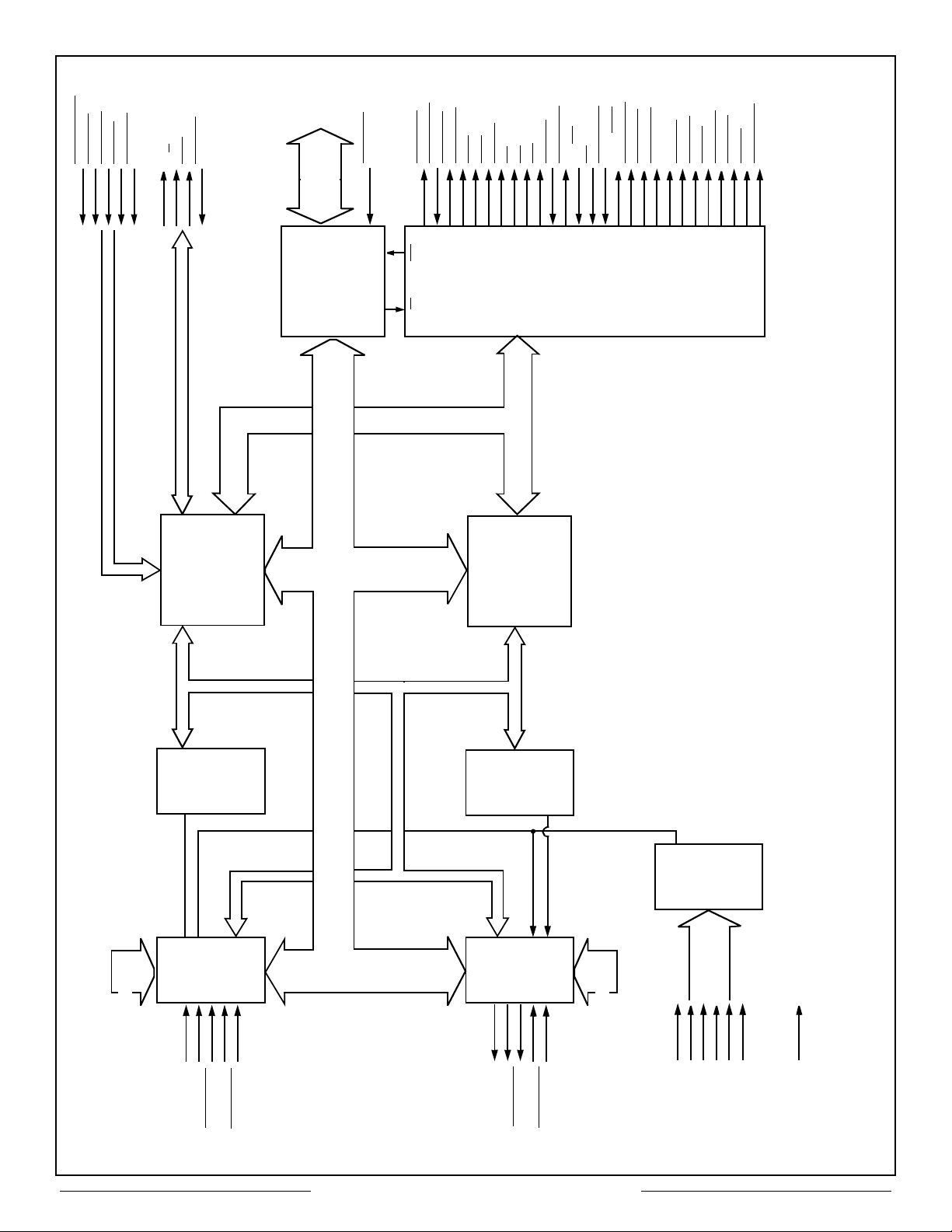
The CT2561 is a 16 MHz single chip dual redundant MIL-STD-1553 Bus Controller (BC), Remote
Terminal Unit (RTU) and Bus Monitor (MT). Packaged in a hybrid plug-in or flatpack, the CT2561
performs all the functions required to interface a MIL-STD-1553 dual redundant serial data bus such
as ACT4487 and a subsystem parallel three-state data bus.
Using a single Aeroflex custom monolithic ASIC design, the CT2561 features pin-for-pin and
functional CT2565 compatibility, user initiated self-test, and low power consumption.
Compatible with most microprocessors the CT2561 provides a 16bit three-state parallel data bus
and uses direct memory access (DMA type) handshaking for subsystem transfers. All message
transfer timing, DMA and control lines are provided internally, thereby reducing the subsystem
overhead associated with message transfers.
The CT2561 implements all dual redundant MIL-STD-1553 mode codes. In addition, any mode
code may (Optionally) be legalized through the use of an external PROM. Complete error detection
is provided by the CT2561 for BC and RTU operation. Error detection includes: response time-out,
inter-message gaps, sync, parity, Manchester, word count and bit count.
The CT2561 is fully compliant with MIL-STD-1553, is available screened in accordance with the
requirements of MIL-STD-883 and operates over the full military temperature range of -55°C to
+125°C.
eroflex Circuit Technology – Data Bus Modules For The Future © SCDCT2561 REV A 8/16/99
Page 2
Aeroflex Circuit Technology
SCDCT2561 REV A 8/16/99 Plainview NY (516) 694-6700
BUSGRNT
BUSREQ
SOM
BUSACK
INCMD
EOMOECS
WR
CHA/CHB
BCSTART
MSGERR
LOOPERR
LWORD
STATERR
STATEN
HSFAIL
NBGRNT
BITEN
NODT
ADRINC
BSCTRCV
TIMEOUT
I/O LOGIC
BUFFERS
BUFENA
I/O0 - I/O16
LMC
WC0-WC4
ILLCMD
T/R
SERREQ
DBACCEPT
SSBUSY
SSERR
SSFLAG
DATA
BUFFERS
REMOTE
TERMINAL
LOGIC
BUS
CONTROLLER
LOGIC
DATA BUS
STATUS INPUTS
MODE CODE CONTROL
CH B
CONTROL
CH A
ENCODE/
DECODE
CH B
ENCODE/
DECODE
TXDATA A
TXINH A
RXDATA A
RXDATA A
TXDATA A
RTADDR
PARITY
CHECKER
TXDATA B
TXINH B
RXDATA B
RXDATA B
TXDATA B
RTADDR
RTADDR
RTADR2
RTADR0
RTADR4
RTADR3
RTADR1
RTADRP
CONTROL BUS
Figure 1 – CT2561 Block Diagram
16MHz
MT
RT/BC
TESTOUT
TESTIN
CH A
CONTROL
I/O BUS
ENR/W
2
Page 3
Aeroflex Circuit Technology
SCDCT2561 REV A 8/16/99 Plainview NY (516) 694-6700
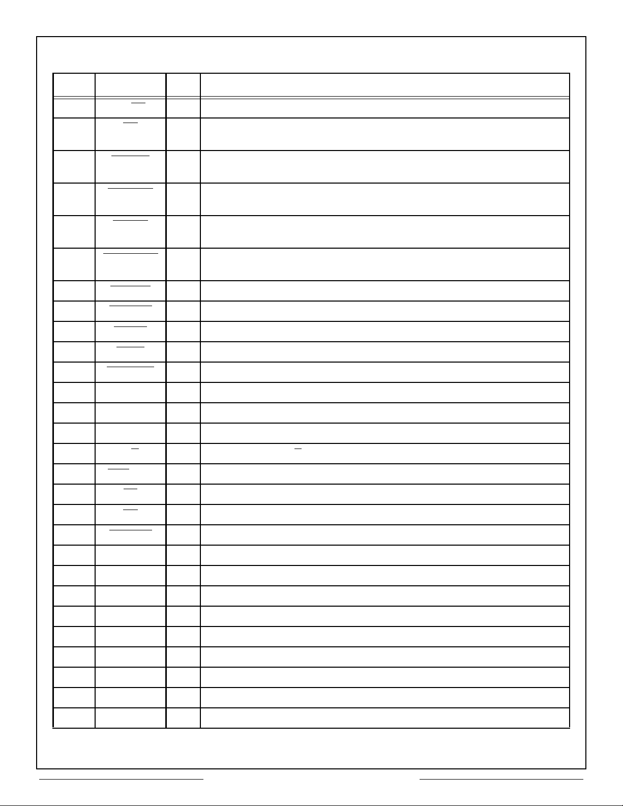
Table 1A – Pin Function Table (78 Pin Plug-In)
Pin # Symbol I/O Description
1 RT/BC
2 MT
I Mode Select input - logic "1" for RT mode, logic “0” for BC mode.
I Monitor mode enable. When unit is operating as a BC, a logic “0” will select
monitor mode.
3 STATEN
O Output signal in RT mode that indicates status word is being transferred on the
internal bus.
4 TIMEOUT
O Indicates No Response Timeout has occurred during BC and RTU (RT to RT
transfer).
5 HSFAIL
O Output in RT mode indicating the DMA transfer did not occur in time to allow
proper operation on the 1553 bus.
6 DBACCEPT
I Input signal used to set DBACCEPT bit in status register for response to a valid
mode command on the 1553 bus.
7 SSFLAG
8 SVCREQ
9 INCMD
10 SSER
11 TESTOUT
I Input which controls the SSFLAG bit in the status register.
I Input which controls the service request bit in the status word.
O Output signal indicating the RT is currently in a message transfer sequence.
I Input which controls the subsystem error bit in the status register.
- Factory test point. Do not connect.
12 WC1 O WC bit 1 - latched output of command word.
13 WC3 O WC bit 3 - latched output of command word.
14 TXINH B O Transmitter inhibit output for channel B.
15 T/R
16 CHA
/CHB O Output indicating current selected channel (0 = Channel A).
17 CS
18 OE
19 BUSREQ
O Output indicating T/R bit of current command word in RT mode.
O Chip Select output for subsystem memory control.
O Output Enable output for subsystem memory control.
O Output signal used to initiate transfer to/from subsystem.
20 +5V I +5 Volt DC input.
21 DB0(LSB) I/O Least significant bit - 16 bit parallel data bus.
22 DB2 I/O Bit 2 of data bus.
23 DB4 I/O Bit 4 of data bus.
24 DB6 I/O Bit 6 of data bus.
25 DB8 I/O Bit 8 of data bus.
26 DB10 I/O Bit 10 of data bus.
27 DB12 I/O Bit 12 of data bus.
28 DB14 I/O Bit 14 of data bus.
3
Page 4

Aeroflex Circuit Technology
SCDCT2561 REV A 8/16/99 Plainview NY (516) 694-6700
Table 1A – Pin Function Table (78 Pin Plug-In) (continued)
Pin # Symbol I/O Description
29 LWORD - Last word output during BC mode indicates last data word of the current
message transfer has been transferred on the parallel bus.
30 MSGERR
O Output signal which indicates an error occurred during the current message
sequence.
31 TXDATA A O Bipolar serial data output to positive input of bus transceiver.
32 RXDATA A
I Bipolar serial input from negative output of bus transceiver.
33 RTADP I Parity bit input for RT address.
34 RTAD1 I Bit 1 of RT address input.
35 RTAD3 I Bit 3 of RT address input.
36 RESET
37 TXDATA B
I System reset input - resets all inputs in module.
O Bipolar serial data output to negative input bus transceiver.
38 RXDATA B I Bipolar serial data input from positive output of bus transceiver.
39 16MHz I 16MHz TTL clock input.
40 GROUND - Signal ground.
41 BCSTART
42 NBGRNT
I Cycle enable input Logic "0" initiates bus controller message transfer operation.
O New bus grant output from RT indicates beginning of message transfer
sequence.
43 BITEN
O Built in Test enable output indicates RT is transferring BlT word on internal 16 bit
bus.
44 WR
45 BUSGRNT
O Write enable output for control of subsystem memory.
I Bus request input in response to DTREQ. Allows BC/RT to transfer data to
subsystem.
46 LOOPERR
47 SSBUSY
48 ILLCMD
49 ADRINC
O Loop error output. Logic "0" indicates failure of loop back transmitted data.
I Subsystem busy input for RT status word.
I Illegal command input to RT, used to block RT response to an illegal command.
O Increment output pulse. Goes LOW at the completion of each word transfer
to/from subsystem. Can increment external address counter.
50 CHASSIS - Frame ground electricity isolated from signal ground
51 WC0 O LSB of current command word count field.
52 WC2 O Bit 2 of word count field.
53 WC4 O Bit 4 of word count field.
54 TXINH A O Transmitter inhibit output signal for Channel A.
55 LMC O Latched Mode Command. Logic "1" indicates current word command is a mode
code word, WC0-WC4.
56 TESTIN
- Factory test point. Do not connect.
4
Page 5

Aeroflex Circuit Technology
SCDCT2561 REV A 8/16/99 Plainview NY (516) 694-6700
Table 1A – Pin Function Table (78 Pin Plug-In) (continued)
Pin # Symbol I/O Description
57 EOM O End of message output. Logic "0" occurs when BC/RT message is completed.
58 BUFENA
I Buffer enable input, may be driven LOW by STATEN or BITEN if subsystem
must read bit or Status words. Enables internal 16 bit bus onto subsystem bus.
59 BUSACK
O Bus acknowledge output. LOW during DMA Handshake, in response to
BUSGRNT
.
60 DB1 I/O Bit 1 of 16 bit parallel bus.
61 DB3 I/O Bit 3 of 16 bit parallel bus.
62 DB5 I/O Bit 5 of 16 bit parallel bus.
63 DB7 I/O Bit 7 of 16 bit parallel bus.
64 DB9 I/O Bit 9 of 16 bit parallel bus.
65 DB11 I/O Bit 11 of 16 bit parallel bus.
66 DB13 I/O Bit 13 of 16 bit parallel bus.
67 DB15(MSB) I/O Bit 15 of 16 bit parallel bus.
68 STATERR
O BC output indicates one or more bits set or address mismatch in a received
status word.
69 TXDATA A
O Bipolar serial data output to negative input of bus transceiver.
70 RXDATA A I Bipolar serial data input from positive output of bus transceiver.
71 NODT
O No data input. Logic "0" indicates the 1553 bus is idle; HIGH means device front
end is active.
72 RTAD0 I LSB of 5 bit RT address.
73 RTAD2 I Bit 2 of RT address.
74 RTAD4 I Bit 4 of RT address.
75 BCSTRCV
O Broadcast receive. Logic "0" means the current command was a broadcast
command.
76 TXDATA B O Bipolar serial output to positive input of bus transceiver.
77 RXDATAB
78 SOM
I Bipolar serial input from negative output of bus transceiver.
O Start of message output indicates beginning of RT/BC message transfer
sequence.
5
Page 6

Aeroflex Circuit Technology
SCDCT2561 REV A 8/16/99 Plainview NY (516) 694-6700
Table 1B – CT2561 Pin Out Description
(Plug-In)
1
41
2
42
3
43
4
44
5
45
6
46
7
47
8
48
9
49
10
50
11
51
12
52
13
53
14
54
15
55
16
56
17
57
18
58
19
59
20
RT/BC
BCSTART
MT
NBGRNT
STATEN
BITEN
TIMEOUT
WR
HSFAIL
BUSGRNT
DBACCEPT
LOOPERR
SSFLAG
SSBUSY
SVCREQ
ILLCMD
INCMD
ADRINC
SSER
CASE GND
TESTOUT
WC0
WC1
WC2
WC3
WC4
TXINH B
TXINH A
T/R
LMC
CHB/CHA
TESTIN
CS
EOM
OE
BUFENA
BUSREQ
BUSACK
+5 Volt
CT2561
MIL-STD-1553
BUS Controller,
Remote Terminal and
BUS MONITOR
DB0
DB1
DB2
DB3
DB4
DB5
DB6
DB7
DB8
DB9
DB10
DB11
DB12
DB13
DB14
DB15 (MSB)
LWORD
STATERR
MSGERR
TXDATA A
TXDATA A
RXDATA A
RXDATA A
NODT
RTADP
RTAD0
RTAD1
RTAD2
RTAD3
RTAD4
RESET
BCSTRCV
TXDATA B
TXDATA B
RXDATA B
RXDATA B
16MHz
SOM
GND
21
60
22
61
23
62
24
63
25
64
26
65
27
66
28
67
29
68
30
69
31
70
32
71
33
72
34
73
35
74
36
75
37
76
38
77
39
78
40
Pin
Function
#
1
RT/BC
2 MT
3 STATEN 42 NBGRNT
4 TIMEOUT 43 BITEN
5 HSFAIL 44 WR
6 DBACCEPT 45 BUSGRNT
7 SSFLAG 46 LOOPERR
8 SVCREQ 47 SSBUSY
9 INCMD 48 ILLCMD
10 SSER 49 ADRINC
11 TESTOUT 50 CASE GND
12 WC1 51 WC0
13 WC3 52 WC2
14 TXINH B 53 WC4
15 T/R
16 CHB/CHA
17 CS
18
OE
19 BUSREQ 58 BUFENA
20 + 5 Volt 59 BUSACK
21 DB0 (LSB) 60 DB1
22 DB2 61 DB3
23 DB4 62 DB5
24 DB6 63 DB7
25 DB8 64 DB9
26 DB10 65 DB11
27 DB12 66 DB13
28 DB14 67 DB15 (MSB)
29 LWORD 68 STATERR
30 MSGERR 69 TXDATA A
31 TXDATA A 70 RXDATA A
32 RXDATA A
33 RTADP 72 RTAD0
34 RTAD1 73 RTAD2
35 RTAD3 74 RTAD4
36 RESET
37 TXDATA B 76 TXDATA B
38 RXDATA B 77 RXDATA B
39 16MHz 78 SOM
Pin
40 GND
41 BCSTART
54 TXINH A
55 LMC
56 TESTIN
57 EOM
71 NODT
75 BCSTRCV
#
Function
Plug-In Pin Connection Diagram, CT2561 and Pinout
6
Page 7

Aeroflex Circuit Technology
SCDCT2561 REV A 8/16/99 Plainview NY (516) 694-6700
Table 2 – CT2561 Pin Out Description
(FP)
1
2
3
4
5
6
7
8
9
10
11
12
13
14
15
16
17
18
19
20
21
22
23
24
25
26
27
28
29
30
31
32
33
34
35
36
37
38
39
40
41
N/C
RT/BC
BCSTART
MT
NBGRNT
STATEN
BITEN
TIMEOUT
WR
HSFAIL
BUSGRNT
DBACCEPT
LOOPERR
SSFLAG
SSBUSY
SVCREQ
ILLCMD
INCMD
ADRINC
SSER
CASE GND
TESTOUT
WC0
WC1
WC2
WC3
WC4
TXINH B
TXINH A
T/R
LMC
CHB/CHA
TESTIN
CS
EOM
OE
BUFENA
BUSREQ
BUSACK
+5V
N/C
CT2561FP
MIL-STD-1553
BUS Controller,
Remote Terminal and
BUS MONITOR
N/C
DB0 (LSB)
DB1
DB2
DB3
DB4
DB5
DB6
DB7
DB8
DB9
DB10
DB11
DB12
DB13
DB14
DB15 (MSB)
LWORD
STATERR
MSGERR
TXDATA A
TXDATA A
RXDATA A
RXDATA A
NODT
RTADP
RTAD0
RTAD1
RTAD2
RTAD3
RTAD4
RESET
BCSTRCV
TXDATA B
TXDATA B
RXDATA B
RXDATA B
16MHz
SOM
GROUND
N/C
82
81
80
79
78
77
76
75
74
73
72
71
70
69
68
67
66
65
64
63
62
61
60
59
58
57
56
55
54
53
52
51
50
49
48
47
46
45
44
43
42
Pin
Function
#
1 N/C 42 N/C
2 RT/BC
3 BCSTART
4 MT 45 16MHz
5 NBGRNT
6 STATEN 47 RXDATA B
7 BITEN
8 TIMEOUT
9 WR 50 BCSTRCV
10 HSFAIL 51 RESET
11 BUSGRNT 52 RTAD4
12 DBACCEPT
13 LOOPERR
14 SSFLAG 55 RTAD1
15 SSBUSY
16 SVCREQ
17 ILLCMD
18 INCMD 59 RXDATA A
19 ADRINC 60 RXDATA A
20 SSER
21 CASE GND 62 TXDATA A
22 TESTOUT 63 MSGERR
23 WC0 64 STATERR
24 WC1 65 LWORD
25 WC2 66 DB15 (MSB)
26 WC2 67 DB14
27 WC4 68 DB13
28 TXINH B 69 DB12
29 TXINH A 70 DB11
30 T/R
31 LMC 72 DB9
32 CHB/CHA
33 TESTIN
34 CS
35 EOM
36 OE
37 BUFENA
38 BUSREQ
39 BUSACK
40 +5V 81 DB0 (LSB)
41 N/C 82 N/C
Pin
43 GROUND
44 SOM
46 RXDATA B
48 TXDATA B
49 TXDATA B
53 RTAD3
54 RTAD2
56 RTAD0
57 RTADP
58 NODT
61 TXDATA A
71 DB10
73 DB8
74 DB7
75 DB6
76 DB5
77 DB4
78 DB3
79 DB2
80 DB1
Function
#
Flat Package Pin Connection Diagram, CT2561 and Pinout
7
Page 8

Aeroflex Circuit Technology
SCDCT2561 REV A 8/16/99 Plainview NY (516) 694-6700
Lead 1 & ESD
Designator
2.100
1.870
.110
1.650
Pin 82
.100
Pin 1
1.500
Pin 21
1.900
Pin 2
Pin 41
Pin 60
Pin 22
.050
.100
TYP
TYP
Pin 19
Pin 39
Pin 20
Pin 59
.018 DIA
TYP
Pin 78
Pin 40
1.800
Figure 2 – Plug In Package Outline
2.200
MAX
.050
.015
Pin 42
.250
MAX
.250
.010
±.002
.180
MAX
Lead 1 & ESD
Designator
Designator
.400
MIN
.095
(4 Places)
1.610
MAX
MAX
Pin 41
2.000
.050 Lead Centers
41 Leads/Side
Figure 3 – Flat Package Outline
8
.080
Page 9

Aeroflex Circuit Technology
SCDCT2561 REV A 8/16/99 Plainview NY (516) 694-6700
CIRCUIT TECHNOLOGY
Ordering Information
Model Number Screening Package
CT2561
CT2561-FP Flat Package
Screened to the individual test methods of MIL-STD-883
Military Temperature, -55°C to +125°C,
Plug in
Aeroflex Circuit Technology
35 South Service Road
Plainview New York 11803
www.aeroflex.com/act1.htm
Specifications subject to change without notice
Telephone: (516) 694-6700
FAX: (516) 694-6715
Toll Free Inquiries: (800) THE-1553
E-Mail: sales-act@aeroflex.com
9
 Loading...