

Page 1
CT 2542 / CT2543
www.aeroflex.com
F
E
I
D
C
E
R
T
A
E
R
O
F
L
E
X
L
A
B
S
I
N
C
.
Dual Redundant Remote Terminal
FOR MIL-STD-1553B
Features
• CT2542 Replaces DDC BUS-65142 and BUS-65144
• CT2543 Replaces DDC BUS-65143 and BUS-65145
• Functions as a Complete Remote Terminal Unit
• Supports 13 Mode Codes, Illegalization of Codes Allowed
• Transfers Data with DMA Type Handshaking
• Latched Outputs for Command Word and Word Count
• 14 Bit Built-ln-Test Word Register
• 4 Error Flag Outputs
• Advanced Low Power VLSI Technology
• DESC SMD# 5962–89798 Approved
CIRCUIT TECHNOLOGY
ISO
9001
I
General Description
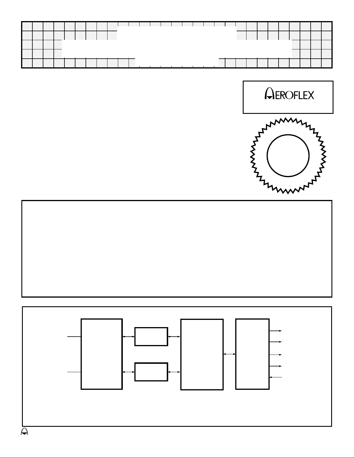
The CT2542 contains 2 transceivers, 2 encoder/decoders, bit processors and complete Remote Terminal (RT)
logic. The device is constructed using Aeroflex advanced VLSI custom chip and hybrid technology. It
functions as a complete dual redundant MIL-STD-1553B RT Unit supporting all 13 mode codes for dual
redundant operation. The CT2542 is a pin-for-pin functional equivalent of the DDC BUS-65142/144 and
performs parallel data transfers with a DMA type handshake. Multiple error flag outputs and host access to
many of the RT Status Word bits are just some of the features that make this part ideal for many RT
applications. The unit has an operating range of -55°C to + 125°C. Aeroflex is a MIL-PRF-38534 Certified
Manufacturer. See "Ordering Information" (last sheet) for CT2543.
DATA BUS A
DATA BUS B
DUAL
TRANSCEIVER
ENCODER/
DECODER
ENCODER/
DECODER
MIL-STD-1553B
PROTOCOL
AND
BIT
PROCESSING
LOGIC
I/O
INTERFACE
DB0-DB15
A0-A11
ERROR FLAG
TIMING FLAGS
STATUS BITS
Figure 1 – Functional Block Diagram
eroflex Circuit Technology – Data Bus Modules For The Future © SCDCT2542 REV E 8/23/00
Page 2
Absolute Maximum Ratings
Parameter Limits Units
Power Supply Voltage (VEE) +0.3 to -18.0 Volts
Power Supply Voltage (V
CCL) -0.3 to +7.0 Volts
Receiver Differential Input ±20 (40Vp-p) Volts
Receiver Input Voltage ±15 Volts
Driver Output Current +200 mA
Transmission Duty Cycle at T
Operating Case Temperature Range (T
C = 125°C 100 %
C) -55 to +125 °C
Power and Thermal Data (Transceiver and Logic Section)
Parameter/Conditions Symbol Min Typ Max Units
Power Supply Voltage
V
EE
V
CCL
-14.25
4.5
-155-15.75
5.5
V
V
Power Dissipation of most critical (hottest) device in
hybrid during continuous transmission (100% Duty
Cycle)
P
C
350 mW
Note 1
Thermal Resistance, most critical device
Ø
JC
60 °C/W
Junction to case temperature rise of most critical device
at 100% duty cycle T
Total supply current standby mode, or transmitting at
less than 1% duty cycle (e.g. 20µs of transmission
every 2ms or longer interval)
Total supply curren transmitting at 1Mhz into a 35-ohm
EE @ 50%
I
load at point A in Figure 2
EE @ 100%
I
I
CCL
I
JC
EE
60 80 °C
mA
mA
Note 2
mA
50
50
70
175
Note 3
270
mA
Note 3
Note 1: Decreases linearly to zero at zero duty cycle.
Note 2: I
Note 3: Decreases linearly to applicable "standby" values at zero duty cycle.
Aeroflex Circuit Technology SCDCT2542 REV E 8/23/00 Plainview NY (516) 694-6700
limit does not change with mode of operation or duty cycle.
CCL
1
Page 3
Electrical Characteristics (Receiver Section)
Parameter/Conditions Symbol Min Typ Max Units
Differential input impedance
DC to 1MHz, Point B, Figure 2
Z
IN
2K Ω
Differential voltage range
Input common mode voltage
range
Common mode rejection ratio
(from point A, Figure 2)
Threshold characteristics
(Sine wave at 1MHz)
Note: Threshold voltages refer to point A, Figure 2.
V
V
DIR
ICR
±20V Vpeak
±10V Vpeak
CMMR 40 dB
V
th
0.6 1.2 Vp-p
Electrical Characteristics (Transmitter Section)
Parameter/Conditions Symbol Min Typ Max Units
Differential output level at point B, Figure 2 (145 ohm load)
Rise and Fall times (10% to 90% of p-p output)
V
T
O
r
24 35 Vp-p
100 300 nS
Output offset at point A in Figure 2 (35-ohm load) 2.5us
after mid-bit crossing of
parity bit of last word of a
660us message
Differential output noise
V
V
OS
NOI
±20 ±90 mV Vpeak
10 mV pp
Aeroflex Circuit Technology SCDCT2542 REV E 8/23/00 Plainview NY (516) 694-6700
2
Page 4

Logic Characteristics
Symbol Parameter Min Typ Max Units Conditions
V
IH
V
IL
I
IL
I
IH
Input l -20 +20 µA Note 2A
I
IL
I
IH
Input l -20 -200 µA
I
IL
I
IH
V
OH
V
OL
Note 1 For INPUT pins 12,13,14,15, 53, 54, 55.
VCC= 5.5V
A. @ VIL = 0.4V
B. @ VIH = 2.4V
Note 2 All remaining INPUTS other than in Note 1.
VCC= 5.5V
A. @ VIL = 0.4V
B. @ VIH = 2.4V
Input "1" 2.4 VDC
Input "0" 0.7 VDC
Input l -80 -400 µA Note 1A
Input l -40 -200 µA Note 1B
Input l -20 +20 µA Note 1B
Input l -40 -400 µA
Output "1" 2.7 VDC Note 3A/4A
Output "0" 0.4 VDC Note 3B/4B
Note 5
Note 3 For OUTPUT pins 4 through 11 and 43 through 50.
A. @ VCC = 4.5V and IOH = 2mA
B. @ VCC = 4.5V and IOL = 4mA
Note 4 All remaining OUTPUTS other than in Note 3.
A. @ VCC = 4.5V and IOH = 1mA
B. @ VCC = 4.5V and IOL = 2mA
Note 5 For INPUT pins 4-11, 43-50.
VCC= 5.5V
A. @ VIL = 0.4V
B. @ VIH = 2.4V
Aeroflex Circuit Technology SCDCT2542 REV E 8/23/00 Plainview NY (516) 694-6700
3
Page 5
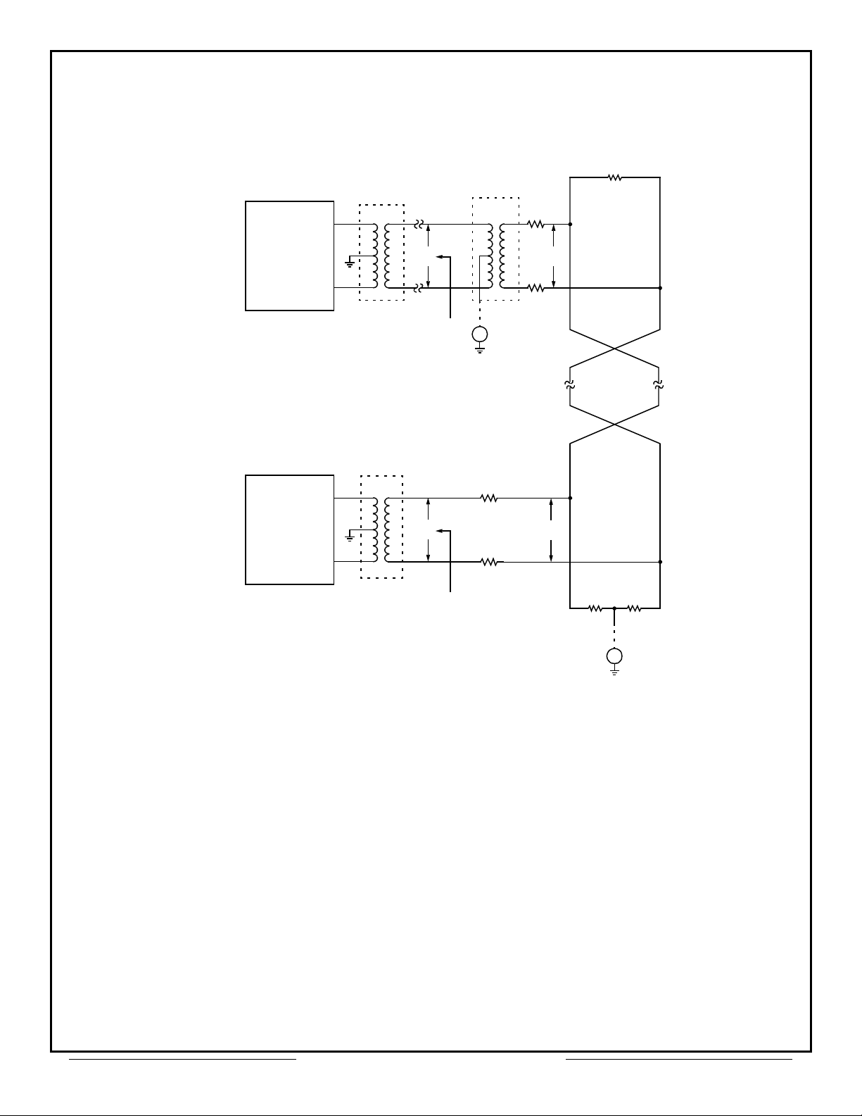
DATA TX/RX
Transformer Coupled Stubs
STUB
2 : 1
ISOLATION
1 : 1.41
55
70Ω
Ω
2542
DATA TX/RX
C
Zoi
Direct Coupled Stubs
STUB
DATA TX/RX
2542
DATA TX/RX
NOTES:
1. Point C, Vo = 18 Vpp Minimum
2. Transformer self Impedance ≥ 3KΩ at 1MHz
CMT for transformer coupled stubs
3. V
CMD for direct coupled stubs
V
1.4 :1
B
55
55Ω
Zoi
A
55Ω
VCMT = ±10 VPK
DC to 2MHZ
Ω
A
35Ω 35Ω
±V
CMD
+
-
Figure 2 – Typical Bus Coupling
Aeroflex Circuit Technology SCDCT2542 REV E 8/23/00 Plainview NY (516) 694-6700
4
Page 6
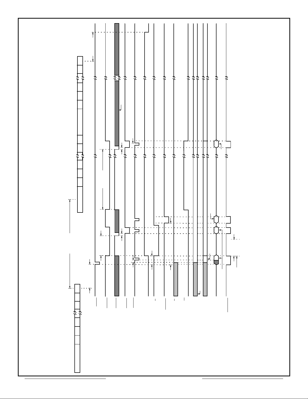
Figure 3 – Timing Diagram, Transmit One Word
NBGT
INCMD
DTREQ
DTGRT
DTACK
STATEN
A5 (D/C)
DTSTB
A11 (T/R)
R/W
A6 - A10
A0 - A4
DB0 - DB4
BUFFENA
TRISTATE
COMMAND WORD
ILLCMD STROBED IN
1.1
µs (STATUS BITS STROBED IN)
(SRQ,BUSY,SSFLAG,RDBC,RTFLAG)
TRISTATE TRISTATE
WORD COUNT
STATUS WORD
DATA WORD FROM SUBSYSTEM
ADDRESS = 00h
ADDRESS = 01h
SUB ADDRESS
PREVIOUS STATE
4.5
µs
1
µs
125n
s
100n
s MAX
2.1µ
s MAX
4.5 ± 0.5µ
s
11µ
s
± .75µ
s
15.5µ
s
max
100n
s MAX
DATA WORD FROM SUBSYSTEM STROBED IN
DON’T CARE
6.5µ
s ±0.5µs
STATUS SYNC 15 14 13 0 P DATA SYNC 15 14 13 0 P
COMMAND SYNC 15 14 13 1 0 P
Aeroflex Circuit Technology SCDCT2542 REV E 8/23/00 Plainview NY (516) 694-6700
5
Page 7

9.5µ
s
± 0.75µ
s
NBGT
INCMD
DTREQ
DTGRT
DTACK
STATEN
A5 (D/C)
DTSTB
A11 (T/R)
R/W
A6 - A10
A0 - A4
DB0 - DB15
BUFFENA
TRISTATE
COMMAND WORD
ILLCMD STROBED IN
1.1
µs (STATUS BITS STROBED IN)
(SRQ,BUSY,SSFLAG,RDBC,RTFLAG)
TRISTATE TRISTATE
WORD COUNT
STATUS WORD
RECEIVE DATA WORD
ADDRESS = 00h
ADDRESS = 01h
SUB ADDRESS
PREVIOUS STATE
1
µs
125n
s
100n
s MAX
2.1µ
s MAX
4.5 ± 0.5µ
s
15.5µ
s
max
100n
s MAX
6.5µ
s ±0.5µs
GBR
STATUS WORD
4.5µ
s
FOR HANDSHAKES < 3.5µ
s
DON’T CARE
STATUS SYNC 8 7 6 5 0 P
4.5 ± 0.5µ
s
250n
s
FOR HANDSHAKES > 3.5µ
s
Figure 4 – Timing Diagram, Receive One Word
COMMAND SYNC 1 0 P DATA SYNC 15 14 13 12 11 0 P
Aeroflex Circuit Technology SCDCT2542 REV E 8/23/00 Plainview NY (516) 694-6700
6
Page 8

NBGT
INCMD
DTREQ
DTGRT
DTACK
STATEN
A5 (D/C)
DTSTB
GBR
R/W
A6 - A10
A11 (T/R)
DB0 - DB15
BUFFENA
TRISTATE
COMMAND WORD
WORD COUNT
ADDRESS = 00h
SUB ADDRESS
PREVIOUS STATE
125n
s
2.1µ
s MAX
4.5 ± 0.5µ
s
100n
s MAX
DON’T CARE
TX STATUS SYNC 15 14 13
TRISTATE TRISTATE TRISTATE
TX COMMAND WORD
4.0 ± 0.5µ
s
250n
s MAX
1µs
A0 - A4
TRANSMITTING RT
RESPONSE TIME
Figure 5 – Timing Diagram, RT to RT Receive One Word (Part A)
RX COMMAND SYNC 15 14 13 1 0 P TX COMMAND SYNC 15 14 13 12 11 10 0 P
Aeroflex Circuit Technology SCDCT2542 REV E 8/23/00 Plainview NY (516) 694-6700
7
Page 9

0 P DATA SYNC 15 14 13 1 0 P
STATUS SYNC 8 7 6 5 1 0 P
NBGT
INCMD
DTREQ
DTGRT
DTACK
STATEN
A5 (D/C)
DTSTB
GBR
R/W
A6 - A10
A11 (T/R)
DB0 - DB15
BUFFENA
500n
s TYP
4.5 ± 0.5µ
s
100n
s MAX
DON’T CARE
TRISTATE
250n
s FOR HANDSHAKES > 3.5µs
A0 - A4
TRISTATE
TX RT STATUS RESPONSE
RECEIVE DATA WORD STATUS WORD
ADDRESS = 01h
4.5 ± 0.5µ
s
4.5 µs
FOR HANDSHAKES < 3.5µs
6.5 ± 0.5µ
s
15.5µ
s MAX
9.5µ
s ±0.75µs
Figure 5 – Timing Diagram, RT to RT Receive One Word (Part B)
Aeroflex Circuit Technology SCDCT2542 REV E 8/23/00 Plainview NY (516) 694-6700
8
Page 10

NBGT
125ns
DTREQ
DTGRT
DTACK
DTSTB
INCMD
A5 (D/C
A11 (T/R
)
)
635ns
1µs
125ns
0ns MIN
125ns
VALID
2.1µs MAX
100ns MAX
375ns
125ns
WHEN T/R = 0
NOTE:
1. R/W
A6 - A10
A0 - A4
WORD
COUNT
SUB ADDRESS
ADDRESS = 00h OR MODE
75ns MAX 75ns MAX
DB0 - DB15
TRISTATE TRISTATETRISTATE
75ns
75ns MAX
MAX
COMMAND WORD
BUFFENA
= LOGIC 0
Figure 6 – TIMING DIAGRAM, COMMAND WORD TRANSFER
Aeroflex Circuit Technology SCDCT2542 REV E 8/23/00 Plainview NY (516) 694-6700
9
Page 11

STATEN
NOTE:
1. R/W
DB0 - DB15
BUFFENA
= LOGIC 0
Figure 7 – Timing Diagram, Status Word Transfer
GBR
DTSTB
Receive Only
375ns
125ns
125ns
75ns
TRISTATE TRISTATE
STATUS
75ns
NOTE:
1. R/W
DB0 - DB15
BUFFENA
= LOGIC 0
BITEN
DTSTB
375 ns
125ns
125ns
75ns
TRISTATE TRISTATE
BIT WORD
75ns
Figure 8 – Timing Diagram, Bit Word Transfer
Aeroflex Circuit Technology SCDCT2542 REV E 8/23/00 Plainview NY (516) 694-6700
10
Page 12

DTREQ
DTGRT
0ns MIN
DON’T CARE
100ns MAX
DTACK
DTSTB
DB0 - DB15
BUFFENA
NOTES:
1. R/W
2. (*) = Non-Mode Only
3. BUFFENA
A0 - A4
= Logic 0
= DTACK
DTREQ
375ns TYP
125ns TYP
125ns TYP
75ns MAX
VALID
75ns MAX
TRISTATE
RECEIVED DATA WORD
50ns MAX
ADDRESS or MODE *ADDRESS +1
Figure 9 – Timing Diagram, Data to Subsystem
0ns MIN
DON’T CARE
DTGRT
DTACK
DTSTB
R/W
DB0 - DB15
TRANSMIT DATA WORD VALID
NOTES:
1. (*) = Non-Mode Only
2. Word Count for Mode Code
3. BUFFENA
A0 - A4
= Don’t Care
Figure 10 – Timing Diagram, Data from Subsystem
100ns MAX
375ns TYP
125ns TYP
125ns TYP
50ns MIN
50ns MAX
50ns MAX
ADDRESS or MODE *ADDRESS +1
Aeroflex Circuit Technology SCDCT2542 REV E 8/23/00 Plainview NY (516) 694-6700
11
Page 13

Figure 11 – Timing Diagram, Data Transfers to Subsystem (No Handshake)
125ns TYP
125ns MIN
125ns MIN
VALID DON’T CAREDON’T CARE
RECEIVED DATA
TRISTATE
ADDRESS OR MODE FIELD
TRISTATE
DTSTB
BUFFENA
DB0 - DB15
A0 - A4
NOTES:
1. R/W = LOGIC 0
2. DTGRT = DTREQ = LOGIC 1
3. INCMD = DAT/CMD ARE LOGIC 1
Aeroflex Circuit Technology SCDCT2542 REV E 8/23/00 Plainview NY (516) 694-6700
12
Page 14

CT2542 Pin Out Description (DDIP)
1
41
2
42
3
43
4
44
5
45
6
46
7
47
8
48
9
49
10
50
11
51
12
52
13
53
14
54
15
55
16
56
17
57
18
58
19
59
20
A10
A9
A8
A7
A6
DB0
DB1
DB2
DB3
DB4
DB5
DB6
DB7
DB8
DB9
DB10
DB11
DB12
DB13
DB14
DB15
+5V
BRO ENA
GND
ADDRE
ADDRD
ADDRC
ADDRB
ADDRA
ADDRP
RTADERR
TXDATA B
TXDATA
-V
B
EE B
N/C
+5V B
GND B
RXDATA
B
RXDATA B
CT2542
MIL-STD-1553B
REMOTE TERMINAL
PROTOCOL UNIT
A3
A2
A1
A0
DTGRT
DTACK
INCMD
A4
HSFAIL
R/W
DISTR
GBR
A5(DAT/CMD)
16MHz IN
RTFAIL
BUF ENA
DTREQ
RESET
ADBC
RTFLAG
TP2
TP1
A11(T/R
BUSY
ILLCMD
SSFLAG
SRQ
ME
BITEN
RXDATA A
RXDATA
A
GND A
+5V A
N/C
EE A
-V
TXDATA
A
TXDATA A
STATEN
NBGT
Pin
21
60
22
61
23
62
24
63
25
64
26
65
27
66
28
67
29
68
30
69
31
70
32
)
71
33
72
34
73
35
74
36
75
37
76
38
77
39
78
40
Function
#
1 A10 40 NBGT
2 A8 41 A9
3 A6 42 A7
4 DB1 43 DB0
5 DB3 44 DB2
6 DB5 45 DB4
7 DB7 46 DB6
8 DB9 47 DB8
9 DB11 48 DB10
10 DB13 49 DB12
11 DB15 50 DB14
12 BRO ENA 51 +5V
13 ADDRE 52 GND
14 ADDRC 53 ADDRD
15 ADDRA 54 ADDRB
16 RTADERR
17 TXDATA
18 N/C 57 -V
19 GND B 58 +5V B
20 RXDATA B 59 RXDATA
21 A3 60 A2
22 A1 61 A0
23 DTGRT
24 INCMD 63 A4
25 HSFAIL
26 DTSTR 65 GBR
27 A5 (DAT/CMD) 66 16MHz IN
28 RTFAIL
29 DTREQ 68 RESET
30 ADBC 69 RTFLAG
31 TP2 (NC) 70 TP1 (NC)
32 A11 (T/R
33 ILLCMD 72 SSFLAG
34 SRQ 73 ME
35 BITEN 74 RXDATA A
36 RXDATA
37 +5V A 76 N/C
38 -V
39 TXDATA A 78 STATEN
EE A 77 TXDATA A
Pin
55 ADDRP
B 56 TXDATA B
62 DTACK
64 R/W
67 BUF ENA
) 71 BUSY
A 75 GND A
#
Function
EE B
B
Figure 12 – DDIP Pin Connection Diagram, CT2542 and Pinout Table
Aeroflex Circuit Technology SCDCT2542 REV E 8/23/00 Plainview NY (516) 694-6700
13
Page 15

CT2542 Pin Out Description (FP)
1
2
3
4
5
6
7
8
9
10
11
12
13
14
15
16
17
18
19
20
21
22
23
24
25
26
27
28
29
30
31
32
33
34
35
36
37
38
39
40
41
N/C
A10
A9
A8
A7
A6
DB0
DB1
DB2
DB3
DB4
DB5
DB6
DB7
DB8
DB9
DB10
DB11
DB12
DB13
DB14
DB15
+5V
BR0 ENA
GND
ADDRE
ADDRD
ADDRC
ADDRB
ADDRA
ADDRP
RTADERR
TXDATA B
TXDATA
-V
B
EE B
N/C
+5V B
GND B
RXDATA
B
RXDATA B
N/C
CT2542-FP
MIL-STD-1553B
REMOTE TERMINAL
PROTOCOL UNIT
N/C
A3
A2
A1
A0
DTGRT
DTACK
INCMD
A4
HSFAIL
R/W
DISTR
GBR
A5(DAT/CMD)
16MHz IN
RTFAIL
BUF ENA
DTREQ
RESET
ADBC
RTFLAG
TP2
TP1
A11(T/R
BUSY
ILLCMD
SSFLAG
SRQ
ME
BITEN
RXDATA A
RXDATA
A
GND A
+5V A
N/C
EE A
-V
TXDATA
A
TXDATA A
STATEN
NBGT
N/C
Pin
82
81
80
79
78
77
76
75
74
73
72
71
70
69
68
67
66
65
64
63
62
61
60
)
59
58
57
56
55
54
53
52
51
50
49
48
47
46
45
44
43
42
Function
#
1 NC 42 NC
2 A10 43 NBGT
3 A9 44 STATEN
4 A8 45 TXDATA A
5 A7 46 TXDATA
6 A6 47 V
7 DB0 48 N/C
8 DB1 49 +5V A
9 DB2 50 GND A
10 DB3 51 RXDATA
11 DB4 52 RXDATA A
12 DB5 53 BITEN
13 DB6 54 ME
14 DB7 55 SRQ
15 DB8 56 SSFLAG
16 DB9 57 ILLCMD
17 DB10 58 BUSY
18 DB11 59 A11 (T/R)
19 DB12 60 TP1
20 DB13 61 TP2
21 DB14 62 RTFLAG
22 DB15 63 ADBC
23 +5V 64 RESET
24 BRO ENA 65 DTREQ
25 GND 66 BUF ENA
26 ADDRE 67 RTFAIL
27 ADDRD 68 16MHz IN
28 ADDRC 69 A5 (DAT/CMD
29 ADDRB 70 GBR
30 ADDRA 71 DTSTR
31 ADDRP 72 R/W
32 RTADERR 73 HSFAIL
33 TXDATA B 74 A4
34 TXDATA
35 -V
36 +15V B 77 DTGRT
37 N/C 78 A0
38 GND B 79 A1
39 RXDATA
40 RXDATA B 81 A3
41 NC 82 NC
EE B 76 DTACK
Pin
B 75 INCMD
B 80 A2
#
Function
EE A
A
A
)
Figure 13 – Flat package Pin Connection Diagram, CT2542 and Pinout Table
Aeroflex Circuit Technology SCDCT2542 REV E 8/23/00 Plainview NY (516) 694-6700
14
Page 16

Plug In Package Outline
Lead 1 & ESD
Designator
2.100
1.870
.110
Pin 1
1.650
Pin 21
Flat Package Outline
Pin 82
.100
1.500
.050
Pin 2
Pin 41
Pin 60
Pin 22
2.200
MAX
1.900
.100
TYP
1.800
.050
TYP
.015
Pin 19
Pin 39
Pin 42
Pin 20
Pin 59
.018 DIA
TYP
Pin 78
Pin 40
.250
MAX
.250
.010
±.002
.181
MAX
1.610
MAX
MAX
Lead 1 & ESD
Designator
Designator
.400
MIN
.095
(4 Places)
2.000
.050 Lead Centers
Pin 41
.080
41 Leads/Side
Aeroflex Circuit Technology SCDCT2542 REV E 8/23/00 Plainview NY (516) 694-6700
15
Page 17

CIRCUIT TECHNOLOGY
Ordering Information
Model Number Screening
CT2542 Military Temperature, -55°C to +125°C,
CT2542-FP - Flat Package
CT2542-701
CT2542-FP-701 - Flat Package
CT2542 - 5962–8979803XA Plug in
CT2542 - 5962–8979803XC Plug in
CT2542-FP - 5962–8979803YA Flat Package
CT2542-FP - 5962–8979803YC Flat Package
CT2543 Military Temperature, -55°C to +125°C,
CT2543-FP - Flat Package
CT2543-701
CT2543-FP-701 - Flat Package
Screened to the individual test methods
of MIL-STD-883
Industrial Temperature, -40°C to +85°C,
No Burn-in
Screened to the individual test methods
of MIL-STD-883
Industrial Temperature, -40°C to +85°C,
No Burn-in
Power
Supplies
+5V & -15V - Plug in
+5V & -12V - Plug in
DESC SMD # Package
- Plug in
- Plug in
CT2543 - 5962–8979804XA Plug in
CT2543 - 5962–8979804XC Plug in
CT2543-FP - 5962–8979804YA Flat Package
CT2543-FP - 5962–8979804YC Flat Package
Aeroflex Circuit Technology
35 South Service Road
Plainview New York 11803
Specifications subject to change without notice.
Aeroflex Circuit Technology SCDCT2542 REV E 8/23/00 Plainview NY (516) 694-6700
16
Toll Free Inquiries: 1-(800)THE-1553
Telephone: (516) 694-6700
FAX: (516) 694-6715
 Loading...