

Page 1
www.aeroflex.com
CT1698
F
E
I
D
C
E
R
T
A
E
R
O
F
L
E
X
L
A
B
S
I
N
C
.
MIL-STD-1397 Type E 10MHz
Low Level Serial Interface
Features
• Optional transformer isolation
• Internally set threshold
• Matched to 50 ohm system impedance power on and off
• Operates with ±5 volt supplies
• Power management
• External output level adjustment
• Accepts synchronous input data
• Unique Manchester decoder requires no clock
• Generates one clock per received bit
• May be used for serial decoding of indefinite word lengths
• Interfaces directly to the CT2500 protocol device
• Other Wire and Fiber Optic types available
General Description
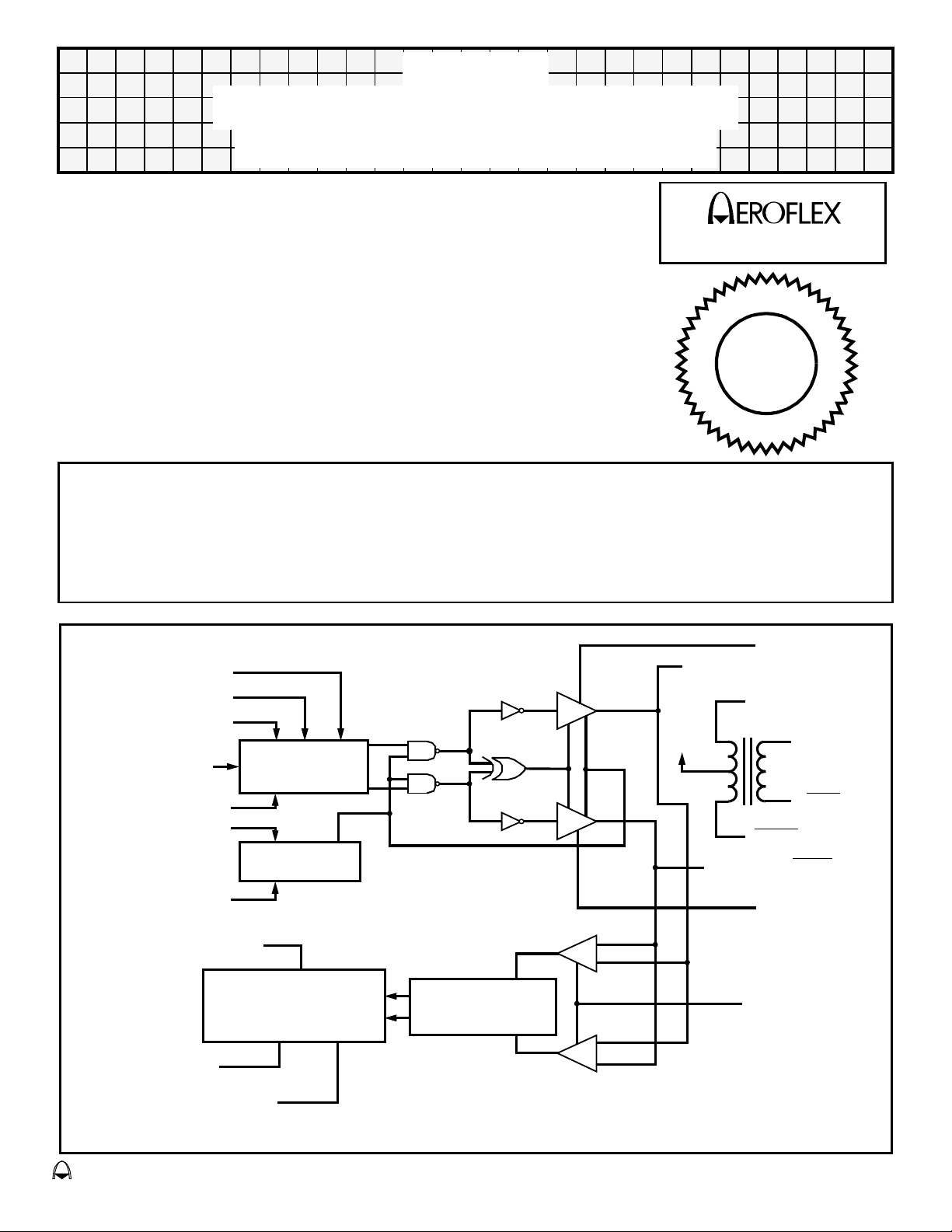
CT1698 is a single hybrid microcircuit which incorporates a serial encoder, transceiver, and Manchester decoder in one package.
The encoder accepts serial NRZ data in conjunction with two synchronous clocks. The CT1698 receiver section accepts bipolar
Manchester encoded signals and passes level detected signals to the serial decoder. The CT1698 has a power management function
and a variable drive level option. The transmitter standby mode is available to reduce the overall power consumption of the CT1698.
The variable drive level output is externally programmable for testing purposes. Aeroflex Circuit Technology is a 80,000 square foot
MIL-PRF-38534 certified facility in Plainview, N.Y.
CIRCUIT TECHNOLOGY
ISO
900
I
1
Serial NRZ Data
10 MHz Shift Clock
20 MHz Gated Clock
Envelope
Master Reset
Encoder Enable
Power Management
Decoded Data Envelope
Clock Regeneration
Clock
R
Serial
Manchester
Encoder
Power
Management
Manchester
Decoder
and
Data
Reconstruction
Drive 1
XFMR SEC/DATA Input
XFMR SEC
Primary
+5V
Primary
XFMR SEC
XFMR SEC/DATA
Drive 2
Rx Strobe
Data
Output
Data
Output
Input
Decoded Data
R
Figure 1 – Block Diagram
eroflex Circuit Technology – Data Bus Modules For The Future © SCDCT1698 REV A 6/12/98
Page 2
Transmission
Reception
The CT1698 accepts synchronous NRZ Data in
conjunction with two clocks signals. The NRZ data
stream is then converted to Manchester code which
is transformer coupled to a 50 ohm Tri-axial cable for
transmission up to 1000 ft.
The transmitter may be placed into standby
condition. This reduces power consumption by
approximately 600mW. Power management is made
available via two standard TTL input pins. The
Receiver is always active and is not affected by the
power management circuitry.
The drive level of the transmitter may be changed
by adding external resistors to the drive pins. These
pins allow the designer to externally program the
transmitter output level from 0.7 to 2.8 Volts peak to
peak.
The transceiver is matched for 50 ohm operation
over a wide band of frequencies. This condition is
maintained with power on and off.
Encoding Timing / Transmitter Specification
The CT1698 receiver section accepts a bipolar
signal which is level detected and passed to the
serial decoder. The decoder section reconstructs
the data and strips the clock from the serial stream.
An NRZ decoded data stream is then produced
synchronously with a recovered clock. The receiver
is designed to meet the MIL-STD-1397 Type E
requirements.
Electrical Requirements
The specification detailed herein encompasses a
hybrid Transceiver/Encoder-Decoder designed to
meet the requirements of the MIL-STD-1397 Type E.
The transceiver is transformer coupled to the
specified triaxial cable.
See Figure 1 for Block Diagram. Inputs and
Outputs are all Synchronous NRZ DATA STREAMS.
The transformer is internal to the package with its
use being optional.
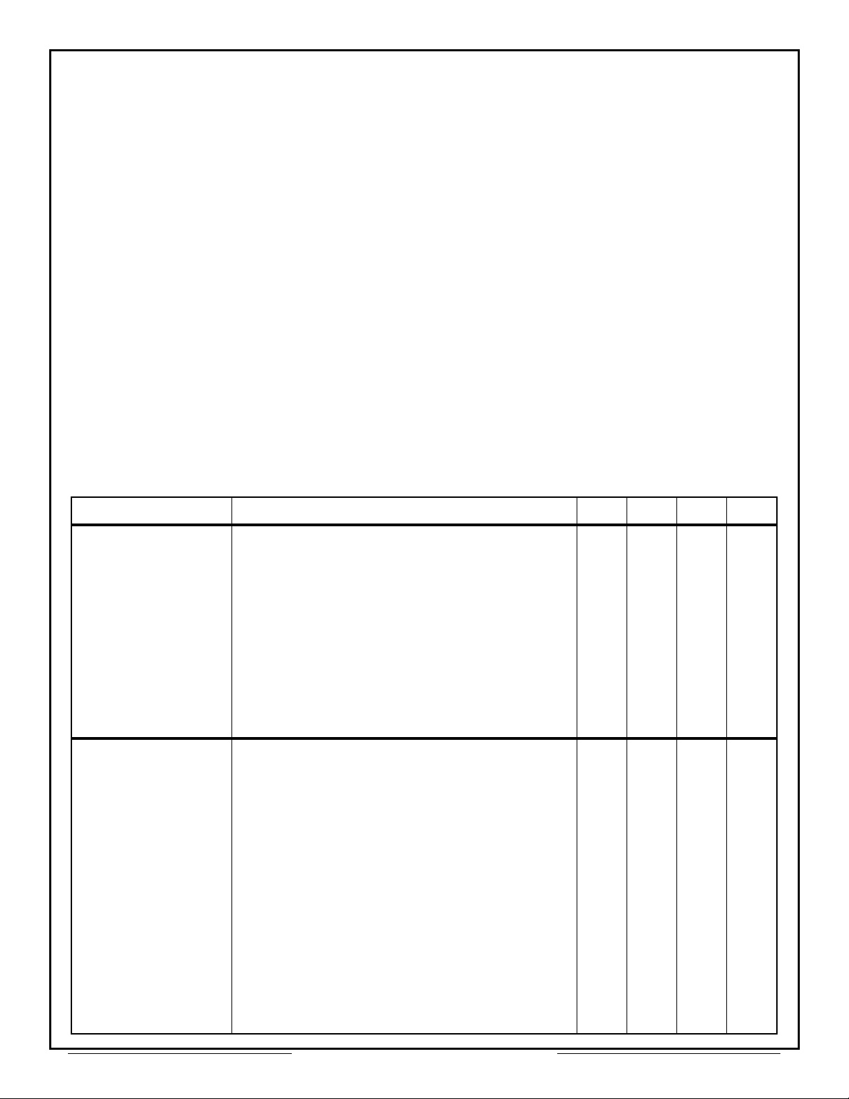
Symbol Parameter / Condition Min Typ Max Unit
Encode Timing
t1 Input data set-up time
t2 Encode clock set-up time
t3 Encode envelope set-up time
t4 Encode envelope turn-off time
t5 Transmitter activation set-up time
t6 Transmitter deactivation hold-time
tw1 20 MHz gated CK pulse width high
tw2 Encoder shift CK pulse width high
Output Signals
Va Output amplitude (see Figure 2)
T Pulse period
Ts Width of 1st positive half bit
Te Width of last half bit
T/2 Half pulse period
Tr Pulse rise time
Tf Pulse fall time
Vs Voltage overshoot
Tos Offset Voltage 2T after last zero crossing
Tdtx Delay from 20 MHz clock input to data output on
TXFMR secondary
Zo Output Impedance
10 40 ns
10 40 ns
10 40 ns
10 35 ns
100 ns
50 ns
20 30 ns
45 55 ns
.45 .7 .8 V
97 100 103 ns
45 65 ns
47 65 ns
47 50 53 ns
.05 .3 V/ns
.05 .3 V/ns
100 mV
30 mV
20 55 ns
45 50 55 Ω
Aeroflex Circuit Technology SCDCT1698 REV A 6/12/98 Plainview NY (516) 694-6700
2
Page 3
Aeroflex Circuit Technology SCDCT1698 REV A 6/12/98 Plainview NY (516) 694-6700
3
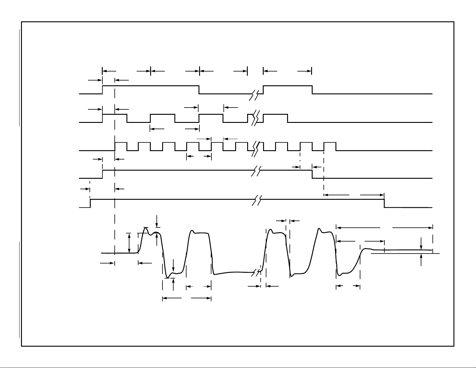
P1 = 50ns ±0.1%
P2 = 100ns ±0.1%
NRZ
BIT NBIT 2BIT 1BIT 0
t
1
Serial Input
t
Encoder
t
2
W2
Shift Clock Input
P2
t
20 MHz
W1
GATED Clock
P1
t
4
NRZ
t
3
Envelope
t
Encoder Enable
5
t
6
Power Management
Pin
T
f
2T
Transmitter
Output
T
dTX
V
a
V
S
V
US
90%
10%
90%
10%
T
T
OS
T/2
T
r
T
Figure 2 Encoder – Transmitter Timing
T
e
Page 4

Manchester II
Receiver Data
1st Data
BIT
2nd Data
BIT
3rd Data
BIT
4th Data
BIT
5th Data
BIT
Decoded
Data
Envelope
R
Data
X
Data
CK
t
1
t
7
R
R
t
2
t
3
t
4
t
5
t
6
t
5
Figure 3 Receiver / Decode Timing
Symbol Parameter / Condition Min Nom Max Units
t1 Envelope delay time - - 100 nsec
t2 Data decode delay - 115 125 nsec
t3 Clock low transition delay - 130 - nsec
t4 Clock
t5 Clock
high time 35 50 65 nsec
R
low time 35 50 65 nsec
R
t6 Envelope off delay 120 - 270 nsec
t7 Receiver strobe enable to input data set-up time 5 nsec
t8 Receiver strobe disable to input data hold-time 20 ?
Power Management Functional Table
Encoder
Enable
(Pin 10)
Power Management
Input
(Pin 9)
Receiver
Status
0 0 Active Standby
X 1 Active Active
1 X Active Active
Power management timing see Figure 2.
Transmitter
Status
Aeroflex Circuit Technology SCDCT1698 REV A 6/12/98 Plainview NY (516) 694-6700
4
Page 5

Drive Level Control Pins
External Resistors may be connected from pins 5 and 6 to VEE or GND to change the Transmitter Output
Level. If pins 5 and 6 are left open the CT1698 operates within the MIL-STD-1397 Type E specification.
Resistors connected from pins 5 and 6 to V
transmitter output offset level.
or Ground must be equal. Unequal resistors will result in a
EE
The formula for peak to peak transmitter output swing with resistors connected between 5 and 6 to V
is:
V
OUT
= 1.39 + 125 ± 15% Volts, R
pk-pk
R
EXT
EXT
> 90Ω
The formula for peak to peak transmitter output swing with resistors connected between pins 5 and 6 to
ground is:
V
OUT
= 1.39 - 50 (VEE -2.5) ± 15% Volts, R
pk-pk
R
EXT
> 180Ω
EXT
Functional Description and Pinout
Pin
Pin Name Function
#
1 XFMR primary/
TX data output
Transformer lead for connection to center conductor of tri-axial
cable
2 XFMR secondary Secondary isolated winding, same phase as center conductor
3 TXDATA output/
Transmitter-receiver I/O pin (usually connected to pin 2)
RX data input
4 No connection
Load or
Drive
EE
5 Drive 2 Output level adjustment selected by resistor to GND or V
6 Drive 1 Output level ajustment selected by resistor to GND or V
EE
EE
7 -5 Volts
8 R
9 Power management
strobe Low level disables receiver 3 S loads
X
Controls transmitter power consumption in conjunction with pin 10 1 S load
input
10 Encoder enable Controls transmitter power consumption in conjunction with pin 9 1 S load
11 Case/signal GND
12 Case/signal GND
13 Decoded data
envelope
High after reception of first half bit; goes low after reception of last
half bit (normally low in inactive state)
4 S drive
14 TP3 test point Alignment point: no electrical connection permitted
15 TP1 test point Alignment point: no electrical connection permitted
16 TP2 test point Alignment point: no electrical connection permitted
17 -5 Volts
18 TP4 test point Alignment point: no electrical connection permitted
19 Clock
R
Reconstructed clock; one clock pulse per input bit received 3 S drive
20 No connection
21 Decoded Data
Aeroflex Circuit Technology SCDCT1698 REV A 6/12/98 Plainview NY (516) 694-6700
R
NRZ reconstructed data. Sampled on clockR rising edge 3 S drive
5
Page 6

Functional Description and Pinout (continued)
Pin
Pin Name Function
#
Load or
Drive
22 No connection
23 +5 volts
24 +5 volts
25 10 MHz encoder shift
One cycle required per data bit. Must be high in first half of bit cell 1 S load
clock
26 NRZ serial input data Serial input to be Manchester encoded with the 20 MHz gated CK 1 S load
27 Encode envelope Must be high to enable transmission; must go low before reception
1 S load
of last 20 MHz positive edge to complete transmission
28 20 MHz gated clock
(encoder)
Each bit to be encoded requires two positive edges of the 20 MHz
CK. These edges must occur at 25ns and 75ns into the bit cell.
1 S load
The end of transmission requires an additional edge in conjunction
29 Master reset
with a logic low on the encode envelope. t
Logic low resets encoder 2 S load
, tF < 5nsec.
R
reset pulse <15 nsec
30 No connection
31 No connection
32 TXDATA output/
RX DATA
input
Transmitter-Receiver I/O pin (usually connected to pin 33)
33 XFMR
34 XFMR
TX DATA
Load and Drive Definitions
1 S load: requires
1 S drive:
Power Consumption
I
CC
I
EE
I
CC
I
EE
secondary Secondary isolated winding, same phase as outer signal
primary/
output
= -2mA max., VIL = 0.8V max
I
IL
= 50µA max., VIH = 2.5V min CIN < 15 pf
I
IH
= 50µA min., VOH = 2.5V min
I
OH
= -2 mA min., VOL = 0.5V max
I
OL
Standby mode 325 450
Standby mode 85 105
100% Transmission 380 510
100% Transmission 125 160
conductor
Transformer lead for connection to outer signal conductor of
tri-axial
Absolute Maximum Ratings
V
(Pins 23, 24) +7 Volts Max
CC
(Pins 7, 17) -7 Volts Max
V
EE
Logic Input Voltage Applied:
Logic Low -1.2V @ 10mA Max
Logic High +5.5 Volts
When used with the internal transformer, the
CT1698 will not be damaged by cable open circuits
or by short circuits of the following types:
Current (mA)
Typ Max
• Line-to-line
• Line-to-ground
• To voltage sources of 0 to 115 volts
alternating current, 60 hertz, line-to-ground
Environmental Parameters
Operating Temperature -55°C to +100°C Case
Storage Temperature -55°C to +150°C
Screened per individual test methods of
MIL-STD-883
Aeroflex Circuit Technology SCDCT1698 REV A 6/12/98 Plainview NY (516) 694-6700
6
Page 7

CIRCUIT TECHNOLOGY
Plainview New York 11830
Toll Free Inquiries: 1-(800)THE-1553
Ordering Information
Model Number Package
CT1698
CT1698FP
Plug-In Package Outline
Pin 1 & ESD
Designator
.270 ±.010
.100 ±.005
TYP
Flat Package Outline
.015 ±.003 .100 ±.005
1.810
MAX
.018 ±.002
DIA
(17 Pins/Side)
.200
.120 ±.010
Both Sides
Plug-in Package
Flat Package
1.200 ±.005
.100 TYP
Both Sides
.180 MAX
.400 MIN
1.410
MAX
Lead 1 & ESD
Designator
1.810
MAX
Aeroflex Circuit Technology
35 South Service Road
Specifications subject to change without notice.
Aeroflex Circuit Technology SCDCT1698 REV A 6/12/98 Plainview NY (516) 694-6700
7
Telephone: (516) 694-6700
FAX: (516) 694-6715
.010 ±.002
 Loading...