

Page 1
www.aeroflex.com
F
E
I
D
C
E
R
T
A
E
R
O
F
L
E
X
L
A
B
S
I
N
C
.
CT1469-2
MIL-STD-1397 Type E 10MHz Transceiver
Features
• Low Level ±0.65V output
• Optional transformer isolation
• Internally set threshold
• Operates with ±5 volt supply
• Matched to 50 ohms system impedance power on or off
• Bipolar construction for radiation resistance
• Power management
• Interfaces directly to the CT1496-2 (Manchester Encoder)
and CT1508-2 (Manchester Decoder)
• MIL-PRF-38534 compliant devices available
General Description
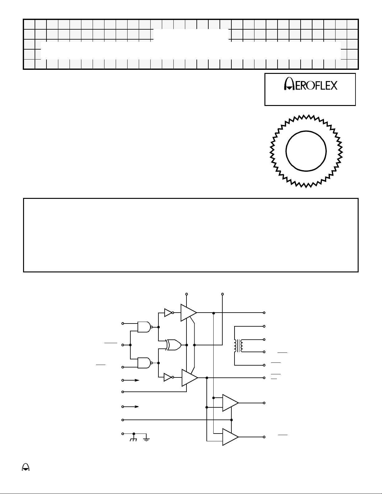
CT1469-2 is a hybrid microcircuit which incorporates a MIL-STD 1397 Type E 10MHz transceiver in
a single package. The transmitter section accepts 10MHZ serial Manchester encoded TTL NRZ data
from the encoder and transformer couples a bipolar ±0.65 volt (nominal) signal level to a 50 ohm
triaxial cable for transmission up to 1000 ft. The CT1469-2 receiver accepts a bipolar signal level
and outputs an NRZ TTL serial data or SIS/SOS signal to the decoder (CT1508-2). Aeroflex Circuit
Technology is a 80,000 square foot MIL-PRF-38534 certified facility in Plainview, N.Y.
CIRCUIT TECHNOLOGY
ISO
900
I
1
TX Data Input
TX Inhibit
TX Data
Input
+5V
Drive 1
-5V
Receiver
Strobe
Digital and Analog
Gnd
Power
Linear
Amp
Linear
Amp
Conditioner
Drive 2
Figure 1 – Block Diagram
Level
Detector
Level
Detector
Xfmr Sec/
RX Data Input
Xfmr Sec
Xfmr Primary/
TX Data Output
Xfmr Primary/
TX Data
Output
Xfmr
Sec
Xfmr
Sec/
RX
Data Input
RX Data
RX Data
eroflex Circuit Technology – Data Bus Modules For The Future © SCDCT1469 REV A 3/22/00
Page 2

Introduction
The specification detailed herein encompasses a hybrid transceiver designed to meet
the requirements of STANAG 4153 and Type E requirements of MIL-STD-1397. The
transceiver is transformer coupled to the specified triaxial cable and is available
compliant to MIL-PRF 38534.
Electrical Requirements
See Figure 1 for block diagram. All input and output signals are manchester encoded.
The transformer is internal to the package with its use being optional.
Aeroflex Circuit Technology SCDCT1469 REV A 3/22/00 Plainview NY (516) 694-6700
2
Page 3
Absolute Maximum Ratings
Parameter Rating Units
Supply Voltage
Vcc
V
EE
Input Voltage
Digital V
Receiver V
IN(D)
IN(R)
+0.5 to +7.0
-0.5 to -7.0
-0.5 to +5.5
±2
V
V
V
V
Power Dissipation P
Storage Temperature Range T
Operating Case Temperature Range T
D 2.0 W
STG -60 to +150 °C
C -55 to +100 °C
DC Electrical Characteristics
(VCC = 5V ±10%, VEE = -5V ±10%, TC = -55 °C to +100°C, unless otherwise specified)
SYMBOL PARAMETER LIMIT
RX DATA (7), RX DATA
V
OH Logic High Output Voltage 2.4V min @ IOH = -80µA, VCC = +4.5V,
V
OL Logic Low Output Voltage 0.4V max @ IOL = 3.2mA, VCC = +4.5V,
(8)
V
EE = -4.5V
V
EE = -4.5V
TX DATA INPUT (22), TX DATA
INPUT (24) 1/
IIH Logic High Input Current 50µA max @ VIH = 2.4V, VCC = +5.5V, VEE
= -5.5V
I
IL Logic Low Input Current -2mA max @ VIL = 0.4V, VCC = +5.5V, VEE
= -5.5V
TX INHIBIT
INPUT (23) 1/
IIH Logic High Input Current 100µA max @ VIH = 2.4V, VCC = +5.5V,
V
EE = -5.5V
I
IL Logic Low Input Current -4mA max @ VIL = 0.4V, VCC = +5.5V, VEE
= -5.5V
Aeroflex Circuit Technology SCDCT1469 REV A 3/22/00 Plainview NY (516) 694-6700
3
Page 4

DC Electrical Characteristics (con’t)
RX STROBE 45 pF max
(VCC = 5V ±10%, VEE = -5V ±10%, TC = -55 °C to +100°C, unless otherwise specified)
SYMBOL PARAMETER LIMIT
RECEIVER STROBE (21) 1/
IIH Logic High Input Current 40µA max @ VIH = 2.4V, VCC = +5.5V,
V
EE = -5.5V
I
IL Logic Low Input Current -3mA max @ VIL = 0.4V, VCC = +5.5V,
V
EE = -5.5V
Power Supply Currents
STANDBY
I
CC VCC = +5.5V, VEE = -5.5V,
V
IEE
23 = GND, V26 = -VEE
90mA max
70mA max
100% Transmission
I
CC VCC = +5.5V, VEE = -5.5V,
V
IEE
Notes:
/ Maximum total capacitance loads allowable on these pins are:
1
DATA, DATA 10 pF max
TX INHIBIT
23 = 2.4V min, fIN = 10MHZ
15 pF max
150mA max
125mA max
Transmitter Timing Characteristics
(VCC = 5V ±10%, VEE = -5V ±10%, TC = -55 °C to +100°C, See Figure 2 and 3, unless otherwise specified)
Symbol Parameter / Condition Min Max Unit
V
A
Output amplitude
T Pulse period 97 103 nsec
T
S Width of 1ST positive half bit 45 65 nsec
1
0.45 0.8 V
T
E Width of last half bit 47 65 nsec
T/2 Half pulse period 47 53 nsec
T
R Pulse rise time 0.05 0.3 V/nsec
T
F Pulse fall time 0.05 0.3 V/nsec
Aeroflex Circuit Technology SCDCT1469 REV A 3/22/00 Plainview NY (516) 694-6700
4
Page 5

Transmitter Timing Characteristics (con’t)
(VCC = 5V ±10%, VEE = -5V ±10%, TC = -55 °C to +100°C, See Figure 2 and 3, unless otherwise specified)
Symbol Parameter / Condition Min Max Unit
VS Voltage overshoot - 100 mV
V
US Voltage undershoot - 100 mV
T
OS Offset Voltage – 2T after last zero crossing - 30 mV
T
DTX Delay from data input to transformer secondary - 50 nsec
V
N Transmitter noise output with transmitter inhibited - 35 mV
Zo Output impedance 45 55
Inhibit External-TTL low inhibits outputs
Internal-Equal input signals inhibit output
1. Pins 25 and 27 are not used for MIL-STD-1397 Type E nominal output signal levels.
Receiver Timing Characteristics
(VCC = 5V ±10%, VEE = -5V ±10%, TC = -55 °C to +100°C, See Figure 4, unless otherwise specified)
Symbol Parameter / Condition Min Max Unit
V
IN Input signal to receiver ±0.22 ±0.88 VPK
VCM Common Mode Rejection
DC to 1.0MHz
2.0MHZ to 20MHz
VT Signal rejection
No response to single ended signals
TD1 Delay from 50% point of positive input
signal to 50% point of data output
-
-
-
-
20
5
-9
10
±0.13
V
PK-TO-PK
VPK-TO-PK
Volts-Seconds
PK
V
- 30 nsec
Ω
T
D2 Delay from 50% point of negative input
- 30 nsec
signal to 50% point of data output
V
O Output signal
Complementary TTL drive capability
of 2 TTL Loads
T
RSU To input data, setup time Receiver Strobe
High
Low
2.4
-
-
0.4
5 - nsec
V
V
Enable
T
RSH Receiver Strobe hold time 20 - nsec
Strobe Strobe – Forces outputs low, logic low
inhibits reception
Aeroflex Circuit Technology SCDCT1469 REV A 3/22/00 Plainview NY (516) 694-6700
5
Page 6

Output Function Table
D D TX INH OUTPUT
D = D
D = D X Inactive
X X 0 Inactive
Active Active 1 Active
Aeroflex Circuit Technology SCDCT1469 REV A 3/22/00 Plainview NY (516) 694-6700
6
Page 7

TX Data Input
Volts
TX Data Input
TX Inhibit
TX Output
VA
PH
PP
VS
S
T
T
50%
V
US
T T/2
DTX
TR
90% 90%
TF
10%
10%
TX Input Requirements
RISE, TFALL < 5nsec
T
P = 100 ±2 nsec
PH = 50 ±2 nsec
2T
T
OS
E
T
T
Figure 2 – Transmitter Logic Waveforms
Shaded Area is acceptable region of operation
100 ±3nsec
V
A Max
0.80
0.45
V
B Min
0
-0.45
50 ±3nsec
0.3 V/nSec
0.30
0.05 V/nSec
-0.40
-0.80
Figure 3 – Transmitter Waveshape Envelope
Aeroflex Circuit Technology SCDCT1469 REV A 3/22/00 Plainview NY (516) 694-6700
7
Page 8

Line to
Line Input
Data
Output
Data
Output
50% 50%
TD1
50%
+.6V
0V
50%
–.6V
D1
T
TD2
VOH
VOL
TD2
V
OH
50%
VOL
Strobe
T
TRSH
3V
0V
RSU
Figure 4 – Receiver Logic Waveforms
Aeroflex Circuit Technology SCDCT1469 REV A 3/22/00 Plainview NY (516) 694-6700
8
Page 9

Pin
#’s
Functions
Pin
#’s
Functions
1
2
3
4
5
6
7
8
9
10
11
12
Vee (-5V)
NC
NC
NC
DIGITAL GND
V
CC (+5V)
RX DATA OUTPUT
RX DATA
OUTPUT
NC
NC
NC
CASE GND (ANALOG)
16
17
18
19
20
21
22
23
24
25
26
27
XFMR PRIMARY/TX DATA OUTPUT
XFMR SEC
XFMR SEC/RX DATA INPUT
NC
NC
RECEIVER STROBE
TX DATA INPUT
TX INHIBIT
TX DATA
INPUT
DRIVE 2
POWER CONDITIONER
DRIVE 1
13
14
15
XFMR
XFMR
SEC/RX DATA INPUT
SEC
XFMR PRIMARY/TX DATA
NC = No Connection
OUTPUT
28
29
30
NC
NC
NC
Aeroflex Circuit Technology SCDCT1469 REV A 3/22/00 Plainview NY (516) 694-6700
9
Page 10

CIRCUIT TECHNOLOGY
Ordering Information
Model Number Package
CT1469-2 Flat Package
Flat Package Outline
1.590 MAX
Lead 1 & ESD
Designator
.015 ±.003 .100 TYP
Specifications subject to change without notice.
(15 Leads/Side on .050 centers)
1.400
1.015
MAX
.450
MIN
.175 MAX
.010 ±.002
Aeroflex Circuit Technology
35 South Service Road
Plainview New York 11803
Aeroflex Circuit Technology SCDCT1469 REV A 3/22/00 Plainview NY (516) 694-6700
10
Toll Free Inquiries: 1-(800)THE-1553
Telephone: (516) 694-6700
FAX: (516) 694-6715
 Loading...