

Page 1
CALIFORNIA MICRO DEVICES
Chip Scale DDR Termination Array
CSPDDR100
Features
• 16 Integrated High frequency Series/Parallel
Terminations
• Ultra small footprint Chip Scale Package
• Ceramic substrate
• 0.35mm Eutectic Solder Bumps, 0.65mm Pitch
Product Description
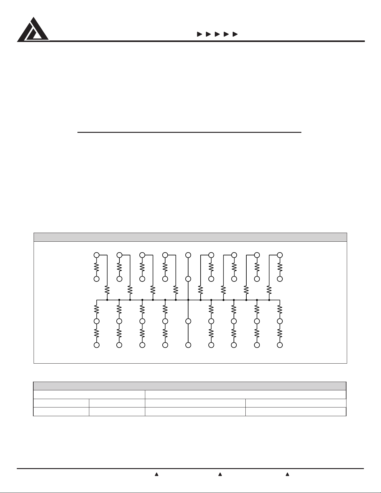
The CSPDDR100 is a high performance Integrated
Passive Device (IPD) which provides Series/Parallel
terminations suitable for use in SSTL and DDR termination applications. Sixteen (16) Series/Parallel termination
channels are provided for a total of 32 integrated
resistors. These resistors provide excellent high frequency performance in excess of 3GHz and are manufactured to an absolute tolerance of ±1%. The Chip
SCHEMATIC DIAGRAM
D
R1
R1
R1
R1
Applications
• DDR Memory bus termination
• SSTL Termination
Scale Package provides an ultra small footprint for
this Integrated Passive Device and provides minimal
parasitics compared to conventional packaging. Typical
bump inductance is less than 25pH. The large solder
bumps and ceramic substrate allow for standard attachment to laminate printed circuit boards without the use
of underfill. The 4X9 Bump pattern is arranged for easy
flow through routing on the pcb.
R1
R1
R1
R1
C
R2
R2
B
R1
A
12 34
R2
R1
R2
R2
R2
R1
R2
R1
R2
R2
5
R2
R2
R1
67 89
R2
R1
R2
R2
R2
R1
NOITAMROFNIGNIREDROTRAPDRADNATS
egakcaP rebmuNtraPgniredrO
elytSspmuBleeR&epaTgnikraMtraP
elacSpihC63001RDDPSC1ApmubkramottodknI
R2
R1
© 2000 California Micro Devices Corp. All rights reserved.
7/21/2000
215 Topaz Street, Milpitas, California 95035 Tel: (408) 263-3214 Fax: (408) 263-7846 www.calmicro.com
C1260700
1
Page 2

CALIFORNIA MICRO DEVICES
Package Diagram (Bumps Up View)
0.65
0.297mm
D
mm
CSPDDR100
5.79mm
0.35mm
Dia.
Bumps
C
B
A
1
23456789
BCPnoeziSdaPmm003.0
epahSdaPdnuoR
noitinifeDdaP )DMSN(sdaPdenifeDksaMredloSnoN
gninepOksaMredloSmm053.0
ssenkcihTlicnetSredloSmm251.0
oitaRxulFredloS05/05
etsaPredloSnaelCoN
hsiniFecarTdnoB)A601sulPuCketnE(PSO
gninepOerutrepAlicnetSredloS).qs(mm063.0
0.65
mm
0.245
mm
2.44mm
0.381mm
0.875mm
SNOITADNEMMOCERDRAOBTIUCRICDETNIRP
Typical PCB Routing Diagram (Bumps Down View)
1
A
B
C
D
©2000 California Micro Devices Corp. All rights reserved.
2
9
7/21/2000215 Topaz Street, Milpitas, California 95035 Tel: (408) 263-3214 Fax: (408) 263-7846 www.calmicro.com
Page 3
CALIFORNIA MICRO DEVICES
(1R )Ω)Ω)Ω)Ω)Ω (2R )Ω)Ω)Ω)Ω)Ω edoC
5205001
eulaVrotsiseR52=1R ,Ω 05=2R ,Ω
RecnareloTetulosbA%1±
srotsiseRfoRCTmpp001±
rotsiseR/gnitaRrewoPWm001
egnaRerutarepmeTgnitarepOC°58otC°04–
CSPDDR100
(seulaVrotsiseR ΩΩΩΩΩ )
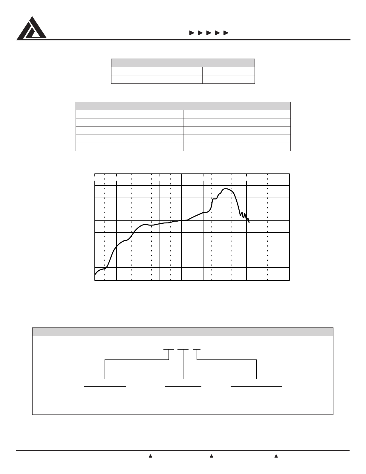
SEULAVDRADNATS
250
225
200
175
C)
o
150
125
100
Temperature (
75
50
25
0 48 97 145
Typical Solder Reflow Thermal Profile (No Clean Flux)
Z4EXH PH Z2 Z3 CD
194 242 290 339 387 435
Time (s)
PART NUMBER KEY
CSP DDR 100
EXHRFZ5
PACKAGE TYPE APPLICATION
CSP = Chip Scale Package DDR = Double Data Rate
© 2000 California Micro Devices Corp. All rights reserved.
7/21/2000
215 Topaz Street, Milpitas, California 95035 Tel: (408) 263-3214 Fax: (408) 263-7846 www.calmicro.com
Memory Termination
Resistor Value Code
100 = R
25Ω; R2 50Ω
1
3
Page 4
CALIFORNIA MICRO DEVICES
Applications
CSPDDR100
The CSPDDR100, Chip Scale DDR Termination Array,
provides sixteen (16) channels of series/parallel termination for SSTL termination applications such as DDR
memory systems. SSTL is the bus standard for DDR
SDRAM systems. Applying terminating resistors to DDR
SDRAM’s interconnections is a necessity to avoid signal
integrity problems in the memory system’s operation.
Improper or no termination on an interconnection that is
a transmission line will cause reflections which in turn
will affect the performance of the system due to ringing,
delays, exceeding IC voltage specifications, or
crosstalk. [1]
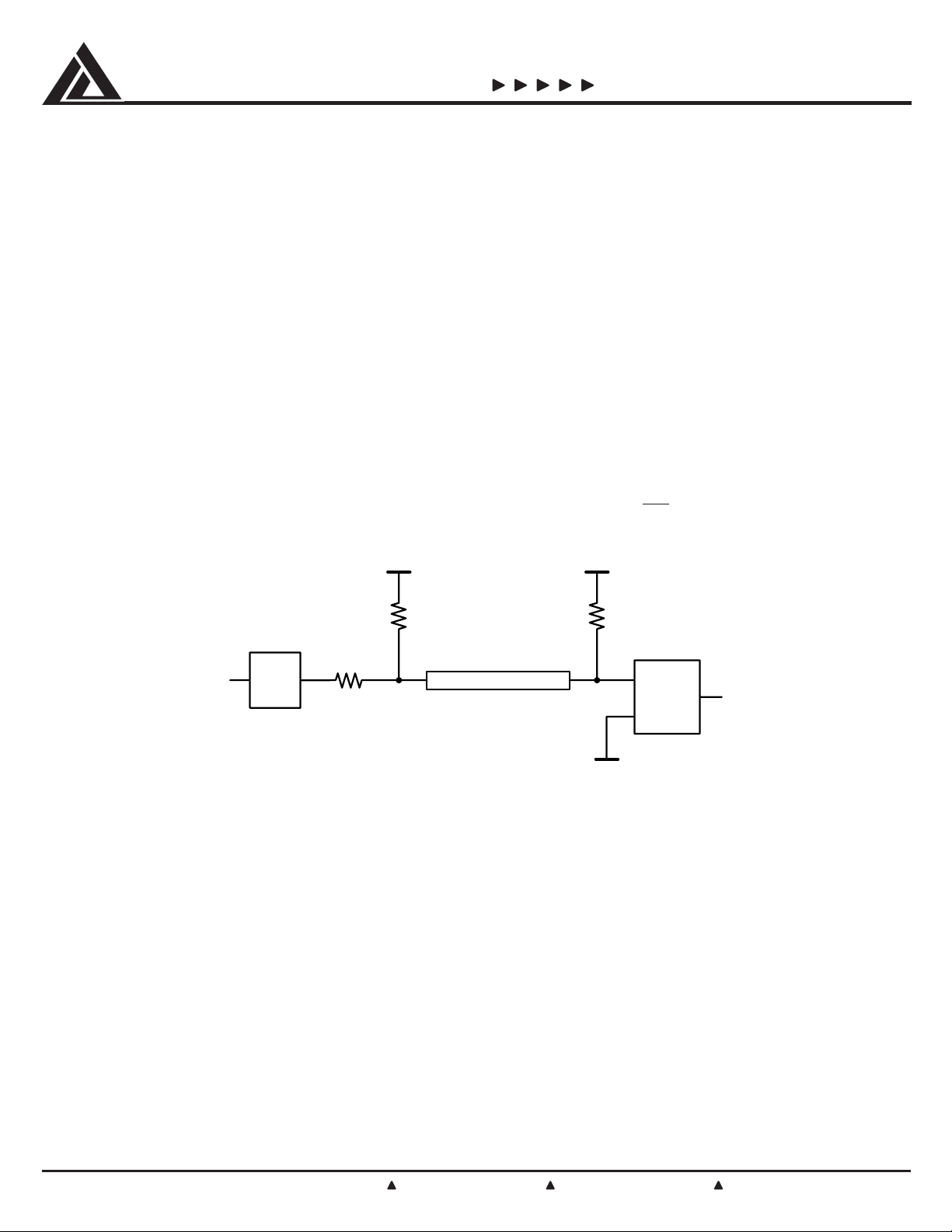
SSTL has four possible configurations. One of them
calls for both a series termination resistor and a parallel
termination at one end of the bus, as shown in Figure 1.
This is the application that the CSPDDR100 satisfies.
When a full level signal is sent down the transmission
line and no reflection is desired, the parallel load
VTT = 0.5 x V
DDQ
RT = 50Ω RT = 50Ω
resistance should equal the characteristic impedance
(Z
) of the transmission line. When a less than full level
0
signal is sent down a transmission line, it is desirable to
have an intentional mismatch of the parallel termination
load resistor so that the higher level reflection voltage
(resulting from having R
> Z0) raises the signal to the
T
full signal level so that load switching occurs in only one
propagation delay time. The use of a series termination
resistor at the source enables the sending of a reduced
level signal on the first incident wave. A reduced level
signal is beneficial in reducing rise times and EMI.
The values of the resistors for DDR/SSTL terminations
are user determined. If values different from the ones in
the CSPDDR100 specification are desired, please
contact California Micro Devices for quotations on other
values.
[1] James Sutherland, “Understanding Transmission Lines, and
High Speed Terminations”,
VTT = 0.5 x V
EDN, October 9, 1999
DDQ
R
V
OUT
SERIES
V
REF
= 0.5 x V
+
–
DDQ
V
IN
Figure 1. SSTL_2 Class II,
Symmetrically Double Parallel Terminated Output Load with Series Resistor
©2000 California Micro Devices Corp. All rights reserved.
4
7/21/2000215 Topaz Street, Milpitas, California 95035 Tel: (408) 263-3214 Fax: (408) 263-7846 www.calmicro.com
 Loading...