

Page 1
CSD04060
TM
ZERO RECOVERY
RECTIFIER
Features Benefits _________
• 600 Volt Schottky Rectifier • Replace Bipolar with Unipolar Rectifiers
• Zero Reverse Recovery • Essentially No Switching Losses
• Zero Forward Recovery • Higher Efficiency
• High Frequency Operation • Reduction Of Rectifier Heat Sink
• Temperature Independent Switching Behavior • Parallel Devices without Thermal Runaway
• Extremely Fast Switching
• Positive Temperature Coefficient on V
F
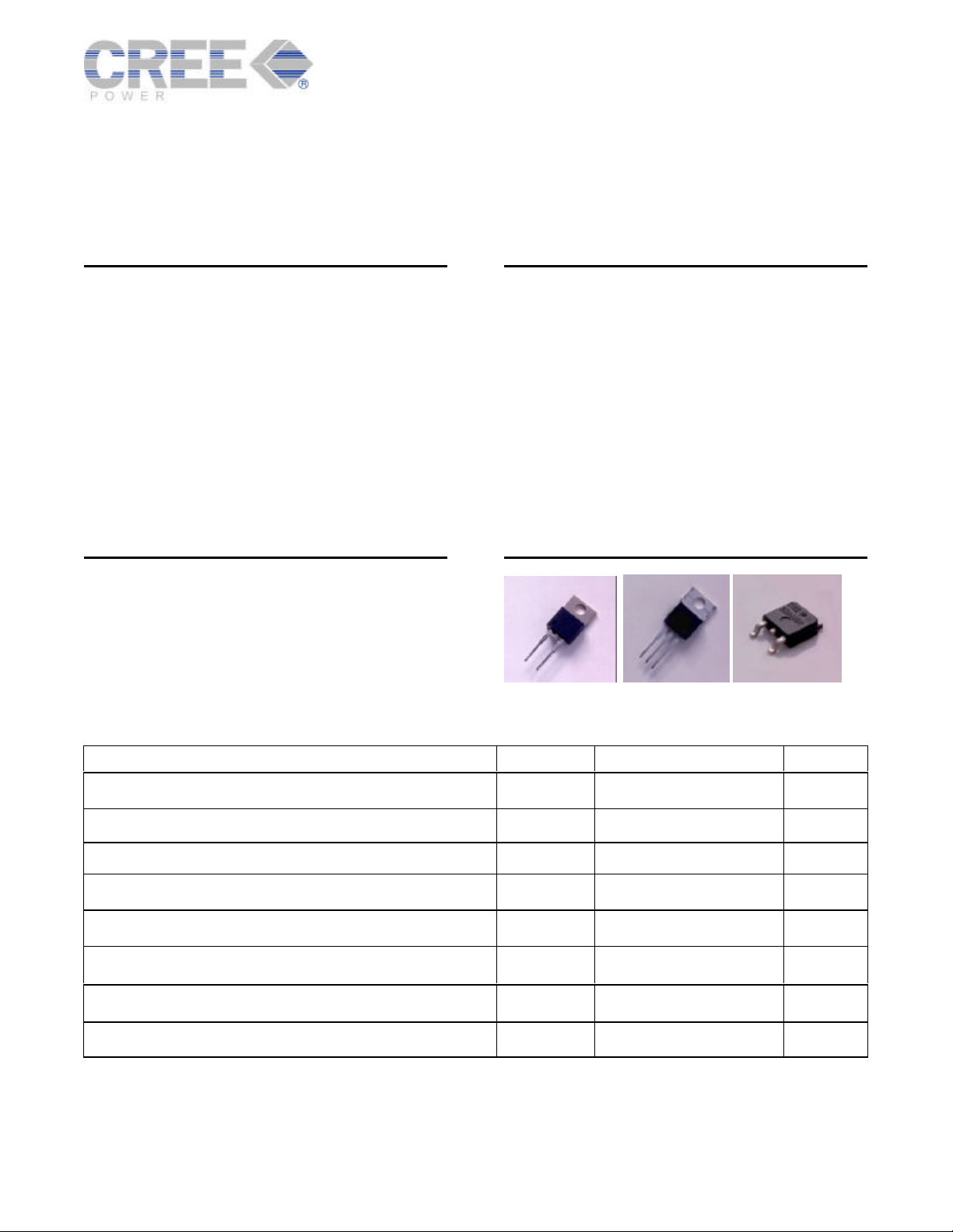
Applications Package ______ ______
• Switch Mode Power Supplies
• Power Factor Correction
• Motor Control
Maximum Ratings
Parameter Symbol Value Unit
Repetitive Peak Reverse Voltage V
Surge Peak Reverse Voltage V
DC Blocking Voltage V
Average Forward Current
TC=150°C
Repetitive Peak Forward Surge Current
TC=25°C, tP=8.3ms, Half Sine Wave
Non-Repetitive Peak Forward Surge Current
TC=25°C, tP=10µs, Pulse
Power Dissipation
TC = 25 °C
I
RRM
RSM
DC
F(AV)
I
FRM
I
FSM
P
tot
600 V
600 V
600 V
4 A
20 A
110 A
62.5 W
Operating Junction and Storage Temperature TJ , T
Page 1 • CSD04060, Rev C
stg
-55 to +175 °C
Page 2
CSD04060
Forward Voltage (V)
ELECTRICAL CHARACTERISTICS
Parameter
Forward Voltage
IF = 4A TJ=25°C
IF = 4A TJ=175°C
Reverse Current
VR = 600V TJ=25°C
VR = 600V TJ=175°C
Symbol Min Typ Max Units
V
F
2.0
25
I
1.6
R
50
1.8
2.4
200
1000
Total Capacitive Charge
VR = 600V,IF = 4A, di/dt = 500 A/µs, TJ = 25°C
Q
C
9 nC
Total Capacitance
VR = 0V, TJ = 25°C, f =1MHz
VR = 200V, TJ = 25°C, f =1MHz
VR = 400V, TJ = 25°C, f =1MHz
C
220
26
20
NOTE:
1. This is a majority carrier diode, so there is no reverse recovery charge.
THERMAL CHARACTERISTICS
Characteristic Symbol Min Typ Max Units
Thermal Resistance from Junction to Case R
θJC
2.4 °C/W
V
µA
pF
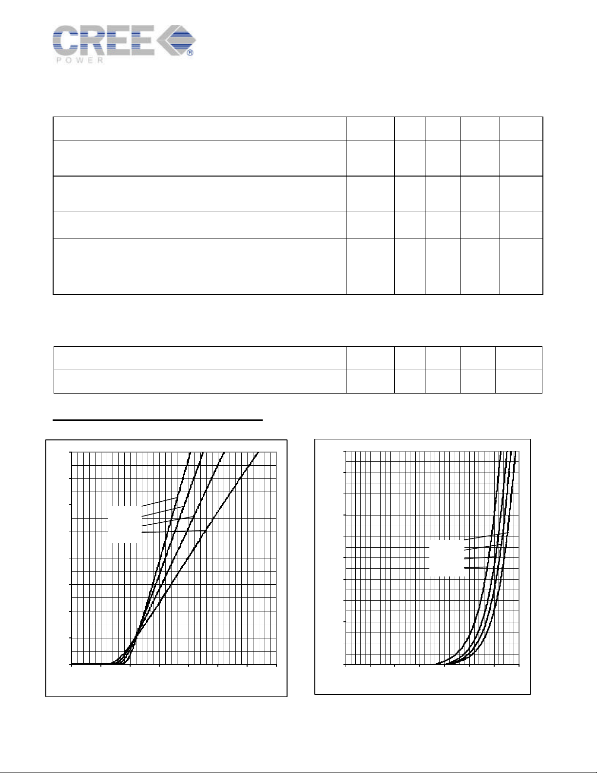
Typical Performance
Figure 1. Forward Characteristics Figure 2. Reverse Characteristics
8
7
6
5
4
3
F
V
2
1
0
0.0 0.5 1.0 1.5 2.0 2.5 3.0 3.5
TJ = 25°C
TJ = 75°C
TJ = 125°C
TJ = 175°C
IF Forward Current (A)
100
90
80
70
A)
µ
60
50
40
Reverse Current (
R
I
30
20
10
0
0 100 200 300 400 500 600 700
VR Reverse Voltage (V)
TJ = 25°C
TJ = 75°C
TJ = 125°C
TJ = 175°C
Page 2 • CSD04060, Rev C
Page 3

CSD04060
Reverse Voltage(V)
C Capacitance (pF)
Zth [°C/W]
Figure 3. Current Derating Figure 4. Capacitance vs. Reverse Voltage
14
12
10
8
6
Forward Current (A)
F(AV)
I
4
2
0
25 50 75 100 125 150 175 200
TC Case Temperature (°C)
Figure 5. Transient Thermal Impedance
160
140
120
100
80
60
40
20
0
1 10 100 1000
V
R
1.00E+01
1.00E+00
1.00E-01
1.00E-02
1.00E-03
1.00E-07 1.00E-06 1.00E-05 1.00E-04 1.00E-03 1.00E-02 1.00E-01 1.00E+00
time [s]
Page 3 • CSD04060, Rev C
Page 4

CSD04060
W
P
A
B
C
F
PIN 1
PIN 2
CASE
NOTE:
Min
Max
Min
MaxA.160
.190
4.06
4.83B.025
.040
0.63
1.02C.015
.022
0.38
0.56
D
.560
.590
14.22
14.99
E
.385
.415
9.78
10.54F.090
.110
2.29
2.79
G
.190
.210
4.83
5.33
H
.045
.055
1.14
1.40J.045
.055
1.14
1.40K.234
.258
5.94
6.55L.090
.115
2.29
2.92
M
.146
.156
3.71
3.96
N
.103
.113
2.62
2.87P.540
.560
13.72
14.22
Q3°7°3°7°
R
.045
.060
1.14
1.52
S
Inches
Millimeters
.243 REF
6.17 REF
NOTE:
PIN 2
PIN 3
CASE
PIN
1 NC
Package Dimensions
Package TO-220-2
D
E
K
H
J
L
N
¡
¡
POS
Q
S
T
G
M
R
U
V
X (2X)
Y
1. Dimension L, M, W apply for Solder Dip Finish.
Inches Millimeters
Min Max Min Max
A .402 .408 10.211 10.364
B .120 .124 3.048 3.150
C .106 .110 2.692 2.794
D .245 .251 6.223 6.375
E .335 .345 8.509 8.763
F .149 .153 3.784 3.886
G .220 .240 5.588 6.096
H .540 .550 13.716 13.970
J
.100 REF 2.540 REF
K .080 2.032
L .050 .056 1.270 1.422
M .032 .038 .813 .956
N .197 .203 5.004 5.156
P .170 .180 4.318 4.572
Q .048 .052 1.219 1.321
R .583 .593 14.808 15.062
S 6.5° 8.5° 6.5° 8.5°
T 6.5° 8.5° 6.5° 8.5°
U 6.5° 8.5° 6.5° 8.5°
V .103 .107 2.616 2.718
W .015 .021 .381 .533
X 2.0° 4.0° 2.0° 4.0°
Y .396 .406 10.058 10.312
----
¡
Package TO-220-3
N
K
P
E
R
H
F
S
B
G
¡
¡
¡
M
Q(5X)
D
C
L
A
J
POS
1. Dimension C apply for Solder Plate Finish.
¡
Page 4 • CSD04060, Rev C
Page 5

CSD04060
ABCDEFGHJKLMNPQRSTU
Min
Max
Min
MaxA.255
.265
6.477
6.731B.197
.205
5.004
5.207C.027
.033
.686
.838
D
.292
.322
7.417
8.179
E
.178
.182
4.521
4.623F.025
.035
.635
.889G44°
46°
44°
46°H.382
.397
9.703
10.084
J
K6°8°6°8°L.086
.094
2.184
2.388
M
.030
.034
.762
.864
N
.040
.044
1.016
1.118
P
.235
.245
5.969
6.223
Q
0.00
.004
0.00
.102
R
S
.017
.023
.428
.588
T
.040
.044
1.016
1.118
U
.021
.027
.534
.686
R0.01TYP
R0.31TYP
Inches
Millimeters
.090TYP
2.286TYP
PIN 1
PIN 2
CASE
Package Dimensions (Cont.)
Package TO-252-2
POS
¡
¡
¡
Part Number Package Marking
CSD04060A TO-220-2 CSD04060
CSD04060B TO-220-3 CSD04060
CSD04060E TO-252-2 SD04060
This product has not been designed or tested for
use in, and is not intended for use in, applications
implanted into the human body nor in applications in
which failure of the product could lead to death,
personal injury or property damage, including but not
limited to equipment used in the operation of nuclear
facilities, life-support machines, cardiac defibrillators
or similar emergency medical equipment, aircraft
navigation or communication or control systems, air
traffic control systems, or weapons systems.
Power Products
4600 Silicon Drive • Durham, NC 27703 • USA
Tel: 919-313-5300 • Fax: 919-313-5451
www.cree.com
Copyright © 2001 Cree, Inc. All rights reserved.
Permission is given to reproduce this document
provided the entire document (including this
copyright notice) is duplicated.
The information in this document is subject to
change without notice.
Cree and the Cree logo are trademarks of Cree, Inc.
Cree, Inc.
Page 5 • CSD04060, Rev C
 Loading...