

Page 1
P O W E R
®
PRELIMINARY CSD01060
TM
ZERO RECOVERY
RECTIFIER
Features Benefits _________
• 600 Volt Schottky Rectifier • Replace Bipolar with Unipolar Rectifiers
• Zero Reverse Recovery • Essentially No Switching Losses
• Zero Forward Recovery • Higher Efficiency
• High Frequency Operation • Reduction Of Rectifier Heat Sink
• Temperature Independent Switching Behavior • Parallel Devices without Thermal Runaway
• Extremely Fast Switching
• Positive Temperature Coefficient on V
F
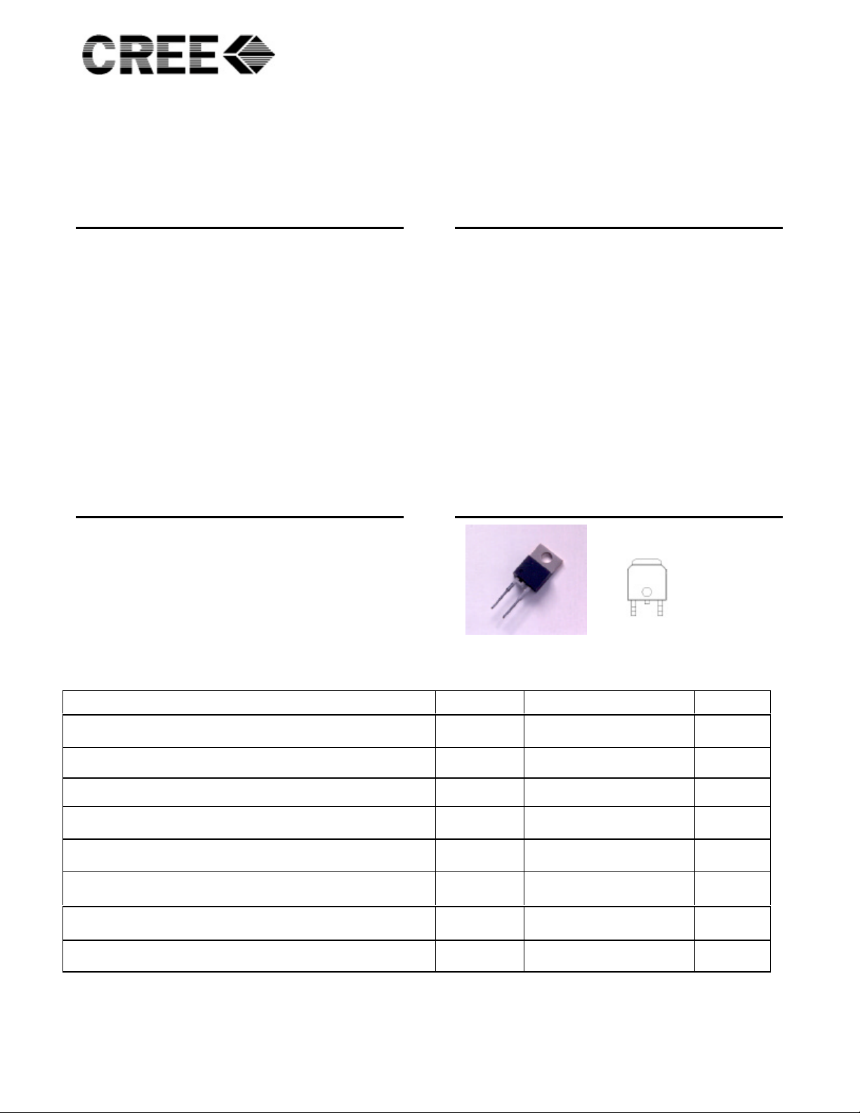
Applications Package _____________
• Switch Mode Power Supplies
• Power Factor Correction
• Motor Control
Maximum Ratings
Parameter Symbol Value Unit
Repetitive Peak Reverse Voltage V
Surge Peak Reverse Voltage V
DC Blocking Voltage V
Average Forward Current
TC=150°C
Repetitive Peak Forward Surge Current
TC=25°C, tP=8.3ms, Half Sine Wave
Non-Repetitive Peak Forward Surge Current
TC=25°C, tp=10µs, Pulse
Power Dissipation
TC = 25°C
I
RRM
RSM
DC
F(AV)
I
FRM
I
FSM
P
tot
600 V
600 V
600 V
1 A
5 A
20 A
21.4 W
Operating Junction and Storage Temperature TJ , T
Page 1 • CSD01060, Rev -
stg
-55 to +175 °C
Page 2
P O W E R
Reverse Voltage (V)
µ
Forward Voltage (V)
F
®
PRELIMINARY CSD01060
ELECTRICAL CHARACTERISTICS
Parameter
Forward Voltage
IF = 1A TJ=25°C
IF = 1A TJ=150°C
Reverse Current
VR = 600V TJ=25°C
VR = 600V TJ=150°C
Symbol Min Typ Max Units
V
F
2.0
20
I
1.6
R
40
1.8
2.4
100
500
Total Capacitive Charge
VR = 600V,IF = 1A, di/dt = 500 A/µs, TJ = 25°C
Q
C
3.3 nC
Total Capacitance
VR = 0V, TJ = 25 °C, f =1MHz
VR = 200V, TJ = 25 °C, f =1MHz
VR = 400V, TJ = 25 °C, f =1MHz
C
80
11
8.5
NOTE:
1. This is a majority carrier diode, so there is no reverse recovery charge.
THERMAL CHARACTERISTICS
Characteristic Symbol Min Typ Max Units
Thermal Resistance from Junction to Case R
Thermal Resistance from Junction to Ambient R
θJC
θJA
7 °C/W
60 °C/W
V
µA
pF
Typical Performance
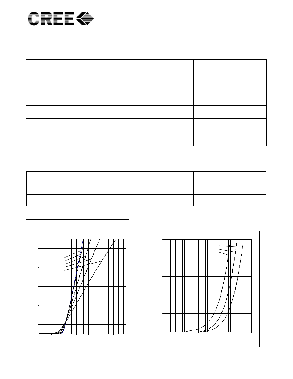
Figure 1. Forward Characteristics Figure 2. Reverse Characteristics
2.0
1.8
1.6
1.4
1.2
1.0
0.8
Forward Current (A)
I
0.6
0.4
0.2
0.0
0.0 0.5 1.0 1.5 2.0 2.5 3.0 3.5
TJ 25 ° C
TJ 50 ° C
TJ 100 ° C
TJ 150 ° C
TJ 200 ° C
V
F
Page 2 • CSD01060, Rev -
50
TJ 25 ° C
TJ 100 ° C
TJ 200 ° C
40
A)
30
20
Reverse Current (
R
I
10
0
0 200 400 600 800 1000
V
R
Page 3

P O W E R
Forward Current (A)
®
PRELIMINARY CSD01060
Figure 3. Current Derating Figure 4. Capacitance vs. Reverse Voltage
1.2
1
0.8
0.6
0.4
F(AV)
I
0.2
0
0 25 50 75 100 125 150 175
TC Case Temperature (°C)
50
45
40
35
30
25
20
C Capacitance (pF)
15
10
5
0
1 10 100 1000
VR Reverse Voltage (V)
Page 3 • CSD01060, Rev -
Page 4

P O W E R
NOTE:
B
A
C
F
PIN 1
PIN 2
CASE
W
P
ABCDEFGHJ
PIN 1
PIN 2
CASE
KLMNPQRST
U
Min
Max
Min
MaxA.255
.265
6.477
6.731B.197
.205
5.004
5.207C.027
.033
.686
.838
D
.292
.322
7.417
8.179
E
.178
.182
4.521
4.623F.025
.035
.635
.889G44°
46°
44°
46°H.382
.397
9.703
10.084
J
K6°8°6°8°L.086
.094
2.184
2.388
M
.030
.034
.762
.864
N
.040
.044
1.016
1.118
P
.235
.245
5.969
6.223
Q
0.00
.004
0.00
.102
R
S
.017
.023
.428
.588
T
.040
.044
1.016
1.118
U
.021
.027
.534
.686
R0.01TYP
R0.31TYP
Inches
Millimeters
.090TYP
2.286TYP
®
PRELIMINARY CSD01060
Package Dimensions
Package TO-220-2
D
E
K
H
J
L
N
¡
¡
Inches Millimeters
POS
A .402 .408 10.211 10.364
Q
S
T
G
M
R
U
V
X (2X)
Y
B .120 .124 3.048 3.150
C .106 .110 2.692 2.794
D .245 .251 6.223 6.375
E .335 .345 8.509 8.763
F .149 .153 3.784 3.886
G .220 .240 5.588 6.096
H .540 .550 13.716 13.970
J
K .080 2.032
L .050 .056 1.270 1.422
M .032 .038 .813 .956
N .197 .203 5.004 5.156
P .170 .180 4.318 4.572
Q .048 .052 1.219 1.321
R .583 .593 14.808 15.062
S 6.5° 8.5° 6.5° 8.5°
T 6.5° 8.5° 6.5° 8.5°
U 6.5° 8.5° 6.5° 8.5°
V .103 .107 2.616 2.718
W .015 .021 .381 .533
X 2.0° 4.0° 2.0° 4.0°
Y .396 .406 10.058 10.312
1. Dimension L, M, W apply for Solder Dip Finish.
Max Min Max
Min
.100 REF 2.540 REF
¡
Package TO-252-2
¡
¡
POS
¡
Page 4 • CSD01060, Rev -
Page 5

P O W E R
®
PRELIMINARY CSD01060
Part Number Package Marking
CSD01060A TO-220-2 SD01060
CSD01060E TO-252-2 SD01060
Cree, Inc.
Power Products
4600 Silicon Drive
Durham, NC 27703 • USA
tel: 919-313-5300
fax: 919-313-5451
www.cree.com
Page 5 • CSD01060, Rev -
Copyright © 2001 Cree, Inc. All rights reserved.
Permission is given to reproduce this document
provided the entire document (including this
copyright notice) is duplicated.
The information in this document is subject to
change without notice.
Cree and the Cree logo are trademarks of Cree,
Inc.
 Loading...