

Page 1
CS8952
CrystalLAN™ 100BASE-X and 10BASE-T Transceiver
Features
! Single-Chip IEEE802.3Physical Interface IC
for 100BASE-TX, 100BASE-FX and
10BASE-T
! Adaptive Equalizer provides Extended
Length Operation (>160 m) with Superior
Noise Immunity and NEXT Margin
! Extremely Low Transmit Jitter (<400 ps)
! Low Common Mode Noise on TX Driver for
Reduced EMI Problems
! Integrated RX and TX Filters for 10BASE-T
! Compensation for Back-to-Back “Killer
Packets”
! Digital Interfaces Supported
– Media Independent Interface (MII) for
100BASE-X and 10BASE-T
– Repeater 5-bit code-group interface
(100BASE-X)
– 10BASE-T Serial Interface
! Register Set Compatible with DP83840A
! IEEE802.3Auto-Negotiationwith Next Page
Support
! Six LED drivers (LNK, COL, FDX, TX, RX,
and SPD)
! Low power (135 mA Typ) CMOS design
operates on a single 5 V supply
Description
The CS8952 uses CMOS technology to deliver a highperformance, low-cost 100BASE-X/10BASE-T Physical
Layer (PHY) line interface. It makes use of an adaptive
equalizer optimized for noise and near end crosstalk
(NEXT) immunity to extend receiver operation to cable
lengths exceeding 160 m. In addition, the transmit circuitry has been designed to provide extremely low
transmit jitter (<400 ps) for improved link partner performance. Transmit driver common mode noise has been
minimized to reduce EMI for simplified FCC certification.
The CS8952 incorporates a standard Media Independent Interface (MII) for easy connection to a variety of 10
and 100 Mb/s Media Access Controllers (MACs). The
CS8952 also includes a pseudo-ECL interface for use
with 100Base-FX fiber interconnect modules.
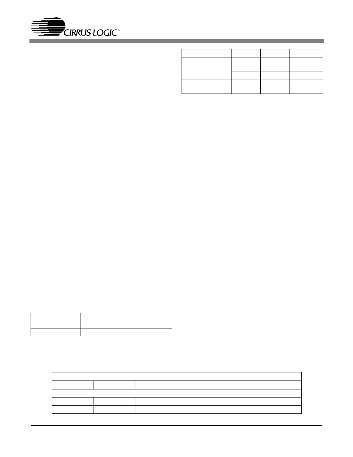
ORDERING INFORMATION
CS8952-CQ 0 to 70 °C 100-pin TQFP
CDB8952 Evaluation Board
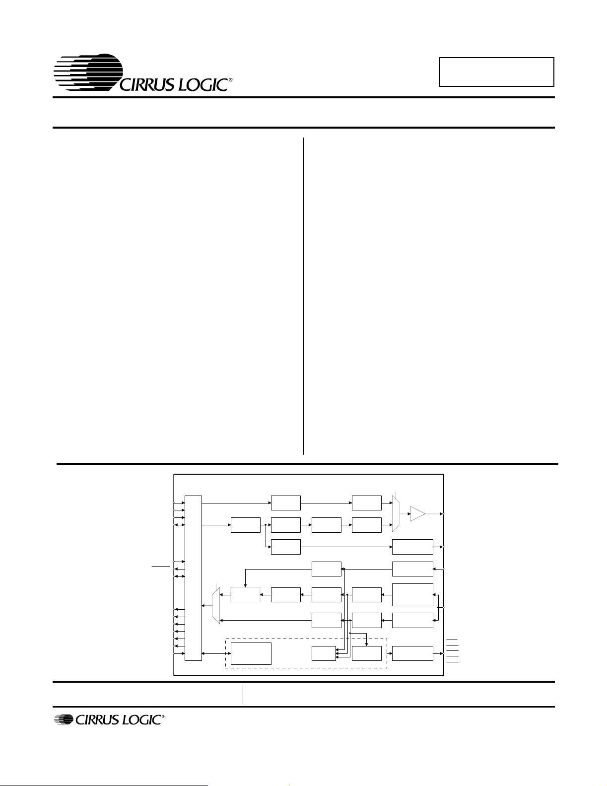
CS8952 10BaseT/100Base-X
Transceiver
TX_EN
TX_ER/TXD4
TXD[3:0]
TX_CLK
MDC
MII_IRQ
MDIO
CRS
COL
RX_ER/RXD4
RX_DV
RXD[3:0]
RX_CLK
RX_EN
10/100
(MII)
M
U
Media Independent Interface
X
Preliminary Product Information
P.O. Box 17847, Austin, Texas 78760
(512) 445 7222 FAX: (512) 445 7581
http://www.cirrus.com
10/100
10BaseT
Filter
Slew Rate
Control
100BaseT
Slicer
10BaseT
Slicer
Auto
Negotiation
M
U
X
ECL Driver
ECL Receiver
Adaptive Eq. &
Baseline Wander
Compensation
10BaseT
Filter
LED
Drivers
TX+,
TX-
TX_NRZ+,
TX_NRZ-
RX_NRZ+,
RX_NRZ-
RX+,
RX-
LED1
LED2
LED3
LED4
LED5
4B/5B
Encoder
4B/5B
Decoder
MII
Control/Status
Registers
Manchester
Encoder
Scrambler
Fiber NRZI
Interface
Descrambler
Link
Management
MLT-3
Encoder
Fiber NRZI
Interface
MLT-3
Decoder
Manchester
Decoder
Timing
Recovery
This document contains information for a new product.
Cirrus Logic reserves the right to modify this product without notice.
Copyright Cirrus Logic, Inc. 2001
(All Rights Reserved)
DS206PP3
1
OCT ‘01
Page 2

TABLE OF CONTENTS
SPECIFICATIONS AND CHARACTERISTICS............................................................. 4
ABSOLUTE MAXIMUM RATINGS .......................................................................4
RECOMMENDED OPERATING CONDITIONS ...................................................4
QUARTZ CRYSTAL REQUIREMENTS ...............................................................4
DC CHARACTERISTICS ..................................................................................... 5
10BASE-T CHARACTERISTICS .........................................................................7
100BASE-X CHARACTERISTICS ....................................................................... 8
100BASE-TX MII RECEIVE TIMING - 4B/5B ALIGNED MODES ........................ 9
100BASE-TX MII RECEIVE TIMING - 5B BYPASS ALIGN MODE ................... 10
100BASE-TX MII TRANSMIT TIMING - 4B/5B ALIGN MODES ........................ 11
100BASE-TX MII TRANSMIT TIMING - 5B BYPASS ALIGN MODE ................ 12
10BASE-T MII RECEIVE TIMING ...................................................................... 13
10BASE-T MII TRANSMIT TIMING ...................................................................14
10BASE-T SERIAL RECEIVE TIMING ..............................................................15
10BASE-T SERIAL TRANSMIT TIMING ............................................................16
AUTO NEGOTIATION / FAST LINK PULSE TIMING ........................................ 17
SERIAL MANAGEMENT INTERFACE TIMING ................................................. 18
INTRODUCTION ..........................................................................................................19
High Performance Analog ...................................................................................19
Low Power Consumption ....................................................................................19
Application Flexibility...........................................................................................19
Typical Connection Diagram ...............................................................................19
FUNCTIONAL DESCRIPTION ....................................................................................21
Major Operating Modes.......................................................................................21
100BASE-X MII Application (TX and FX) ..................................................... 21
Symbol Encoding and Decoding ...........................................................22
100 Mb/s Loopback ............................................................................... 23
100BASE-X Repeater Application ............................................................... 23
10BASE-T MII Application ...........................................................................24
Full and Half Duplex operation .............................................................. 24
Collision Detection ................................................................................. 24
Jabber ................................................................................................... 24
Link Pulses ............................................................................................ 24
Receiver Squelch .................................................................................. 25
10BASE-T Loopback ............................................................................. 25
Carrier Detection ................................................................................... 25
CS8952
Contacting Cirrus Logic Support
For a complete listing of Direct Sales, Distributor, and Sales Representative contacts, visit the Cirrus Logic web site at:
http://www.cirrus.com/corporate/contacts/sales.cfm
Preliminary product information describes products which are in production, but for which full characterization data is not yet available. Advance product information describes products whichare in development and subject to development changes. Cirrus Logic, Inc. has made best effortsto ensure that the information
contained in this document is accurate and reliable. However, the information is subject to change without notice and is provided “AS IS” without warranty of
any kind (express or implied). Customers are advised to obtain the latest version of relevant information to verify, before placing orders, that information being
relied on is current and complete. All products are sold subject to the terms and conditions of sale supplied at the time of order acknowledgment, including those
pertainingto warranty, patent infringement,and limitation of liability. No responsibility is assumed by Cirrus Logic, Inc. for the use of this information, including
use of this information as the basis for manufacture or sale of any items, nor for infringements of patents or other rights of third parties. This document is the
property of Cirrus Logic, Inc. and by furnishing this information, Cirrus Logic, Inc. grants no license, express or implied under any patents, mask work rights,
copyrights, trademarks, trade secrets or other intellectual property rights of Cirrus Logic, Inc. Cirrus Logic, Inc., copyright owner of the information contained
herein, gives consent for copies to be made of the information only for use within your organization with respect to Cirrus Logic integrated circuits or other parts
of Cirrus Logic, Inc. The same consent is given for similar information contained on any Cirrus Logic website or disk. This consent does not extend to other
copying such as copying for general distribution, advertising or promotional purposes, or for creating any work for resale. The names of products of Cirrus Logic,
Inc. or other vendors and suppliers appearing in this document may be trademarks or service marks of their respective owners which may be registered in some
jurisdictions. Alist of Cirrus Logic, Inc. trademarks and service marks can be found at http://www.cirrus.com
2 CrystalLAN™ 100BASE-X and 10BASE-T Transceiver
.
Page 3

10BASE-T Serial Application ....................................................................... 25
Auto-Negotiation ................................................................................................. 25
Reset Operation.................................................................................................. 26
LED Indicators..................................................................................................... 26
MEDIA INDEPENDENT INTERFACE (MII) ................................................................. 27
MII Frame Structure ............................................................................................ 27
MII Receive Data................................................................................................. 28
MII Transmit Data................................................................................................ 28
MII Management Interface .................................................................................. 29
MII Management Frame Structure...................................................................... 29
CONFIGURATION ...................................................................................................... 30
Configuration At Power-up/Reset Time............................................................... 30
Configuration Via Control Pins............................................................................ 30
Configuration via the MII ..................................................................................... 30
CS8952 REGISTERS .................................................................................................. 31
Basic Mode Control Register - Address 00h ..................................................... 32
Basic Mode Status Register - Address 01h ...................................................... 34
PHY Identifier, Part 1 - Address 02h ................................................................. 36
PHY Identifier, Part 2 - Address 03h ................................................................. 37
Auto-Negotiation Advertisement Register - Address 04h .................................. 38
Auto-Negotiation Link Partner Ability Register - Address 05h ........................... 39
Auto-Negotiation Expansion Register - Address 06h ........................................ 40
Auto-Negotiation Next-Page Transmit Register - Address 07h ......................... 41
Interrupt Mask Register - Address 10h ............................................................. 42
Interrupt Status Register - Address 11h ............................................................ 45
Disconnect Count Register - Address 12h ........................................................ 48
False Carrier Count Register - Address 13h ..................................................... 49
Scrambler Key Initialization Register - Address 14h ......................................... 50
Receive Error Count Register - Address 15h .................................................... 51
Descrambler Key Initialization Register - Address 16h ..................................... 52
PCS Sub-Layer Configuration Register - Address 17h ..................................... 53
Loopback, Bypass, and Receiver Error Mask Register - Address 18h ............. 56
Self Status Register - Address 19h ................................................................... 59
10BASE-T Status Register - Address 1Bh ........................................................ 61
10BASE-T Configuration Register - Address 1Ch ............................................ 62
DESIGN CONSIDERATIONS ...................................................................................... 64
Twisted Pair Interface ......................................................................................... 64
100BASE-FX Interface........................................................................................ 64
Internal Voltage Reference ................................................................................. 64
Clocking Schemes .............................................................................................. 65
Recommended Magnetics .................................................................................. 66
Power Supply and Decoupling............................................................................ 66
General Layout Recommendations..................................................................... 66
PIN DESCRIPTIONS ................................................................................................... 69
PACKAGE DIMENSIONS ........................................................................................... 81
CS8952
CrystalLAN™ 100BASE-X and 10BASE-T Transceiver 3
Page 4
CS8952
1. SPECIFICATIONS AND CHARACTERISTICS
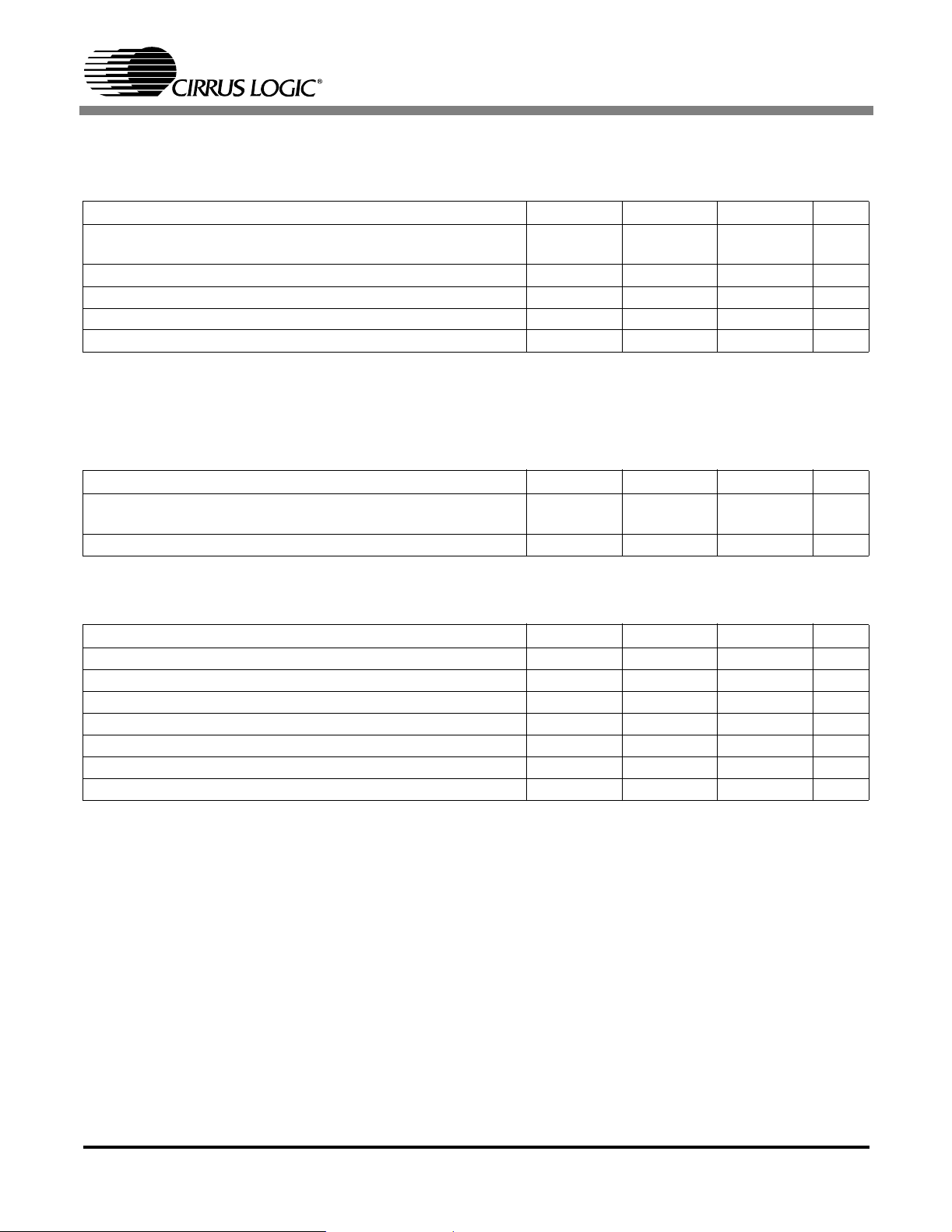
ABSOLUTE MAXIMUM RATINGS (AVSS,DVSS = 0 V, all voltages with respect to 0 V.)
Parameter Symbol Min Max Unit
Power Supply V
Input Current Except Supply Pins - +/-10.0 mA
Input Voltage -0.3 V
Ambient Temperature Power Applied -55 +125 °C
Storage Temperature -65 +150 °C
WARNING: Operation at or beyond these limits may result in permanent damage to the device.
Normal operation is not guaranteed at these extremes.
V
DD_MII
DD
RECOMMENDED OPERATING CONDITIONS (AVSS, DVSS = 0 V, all voltages with respect
to 0 V.)
Parameter Symbol Min Max Unit
Power Supply Core
MII
Operating Ambient Temperature T
V
V
DD_MII
DD
A
-0.3
-0.3
4.75
3.0
070°C
6.0
6.0
+0.3 V
DD
5.25
5.25
V
V
V
QUARTZ CRYSTAL REQUIREMENT S (If a 25 MHz quartz crystal is used, it must meet the fol-
lowing specifications.)
Parameter Min Typ Max Unit
Parallel Resonant Frequency - 25.0 - MHz
Resonant Frequency Error (CL = 15 pF) -50 - +50 ppm
Resonant Frequency Change Over Operating Temperature -40 - +40 ppm
Crystal Load Capacitance - 15 - pF
Motional Crystal Capacitance - 0.021 - pF
Series Resistance - - 18 Ω
Shunt Capacitance - - 7 pF
4 CrystalLAN™ 100BASE-X and 10BASE-T Transceiver
Page 5
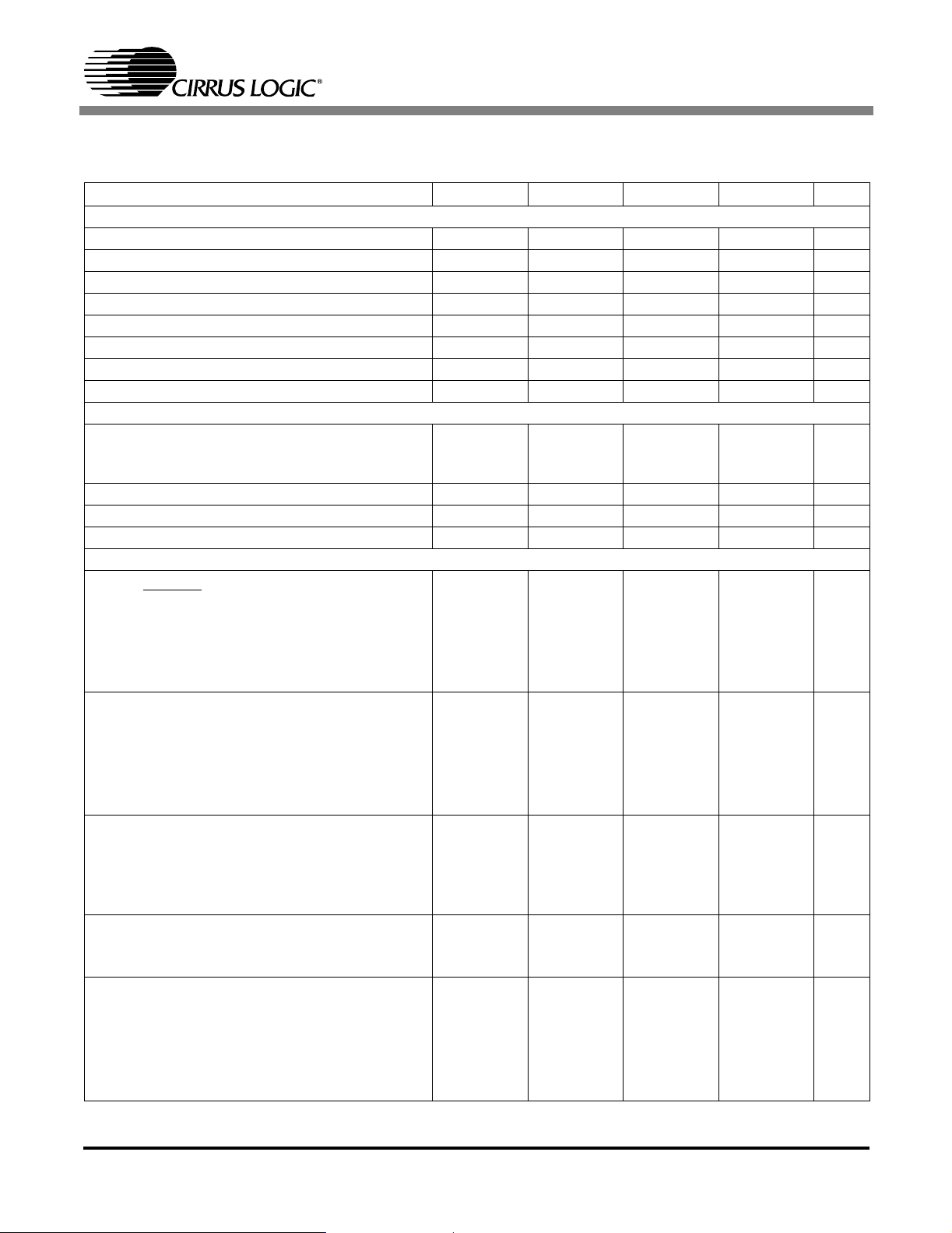
DC CHARACTERISTICS (Over recommended operating conditions)
Parameter Symbol Min Typ Max Unit
External Oscillator
XTAL_I Input Low Voltage V
XTAL_I Input High Voltage V
XTAL_I Input Low Current I
XTAL_I Input High Current I
XTAL_I Input Capacitance C
XTAL_I Input Cycle Time t
XTAL_I Input Low Time t
XTAL_I Input High Time t
Power Supply
Power Supply Current 100BASE-TX (Note 1)
I
100BASE-FX (Note 1)
10BASE-T (Note 1)
Hardware Power-Down (Note 1)I
Software Power-Down (Note 1)I
Low Power Power-Up (Note1)I
DDHPDN
DDSPDN
DDSLPUP
Digital I/O
Output Low Voltage
CLK25, MII_IRQ
, SPD10, SPD100 IOL=4.0mA
V
IXH
IXH
IXL
IXH
L
IXC
IXL
XH
DD
OL
-0.3 - 0.5 V
3.5 - VDD+0.5 V
-40 - - µA
--40µA
39.996 - 40.004 ns
18 - 22 ns
18 - 22 ns
-
-
-
-900-µA
-20-mA
-900-µA
-
CS8952
-35pF
135
90
80
-
145
-
-
0.4
mA
V
LED[4:0] I
Output Low Voltage (MII_DRV = 1)
COL, CRS, MDIO, RXD[3:0],
RX_CLK, RX_DV, RX_ER,
TX_CLK I
VDD_MII = 5V; I
VDD_MII = 3.3V, I
Output Low Voltage (MII_DRV = 0)
COL, CRS, MDIO, RXD[3:0],
RX_CLK, RX_DV, RX_ER,
TX_CLK I
Output High Voltage
CLK25, SPD10, SPD100 I
Output High Voltage (MII_DRV = 1)
COL, CRS, MDIO, RXD[3:0],
RX_CLK, RX_DV, RX_ER,
TX_CLK I
VDD_MII=5V;I
VDD_MII=3.3V,I
OH
OH
=10.0mA
OL
=4.0mA
OL
=43.0mA
OL
=26.0mA
OL
=4.0mA
OL
=-4.0mA
OH
=-4.0mA
OH
=-20.0mA
=-20.0mA
-
V
OL
-
-
-
V
OL
-
0.4
V
-
-
-
0.4
3.05
2.1
V
--0.4
V
OH
V
2.4 - -
V
OH
2.4
1.1
1.1
-
-
-
-
-
-
V
CrystalLAN™ 100BASE-X and 10BASE-T Transceiver 5
Page 6
DC CHARACTERISTICS (CONTINUED) (Over recommended operating conditions)
Parameter Symbol Min Typ Max Unit
Output High Voltage (MII_DRV = 0)
COL, CRS, MDIO, RXD[3:0],
RX_CLK, RX_DV, RX_ER,
TX_CLK I
=-4.0mA
OH
V
OH
2.4 - -
CS8952
V
Input Low Voltage
All Inputs Except AN[1:0], TCM, TXSLEW[1:0]
Input High Voltage
All Inputs Except AN[1:0], TCM, TXSLEW[1:0]
Tri-Level Input Voltages
AN[1:0], TCM, TXSLEW[1:0]
Input Low Current
MDC, TXD[3:0], TX_CL K, TX_EN,
TX_ER V
MDIO V
=0.0V
I
=0.0V
I
Input High Current
MDC, TXD[3:0], TX_CL K, TX_EN,
TX_ER V
MDIO V
=5.0V
I
=5.0V
I
V
IL
V
IH
V
IL
--0.8V
2.0 - - V
-
-
1/3 V
DD_MII
V
-20%
V
IM
1/3 V
DD_MII
-
+20%
V
IH
2/3 V
DD_MII
-
2/3 V
-20%
DD_MII
-
+20%
I
IL
-20
-3800
I
IH
-
-
-
-
-
-
-
-
200
20
µA
µA
Input Leakage Current
All Other Inputs 0<=V<=V
DD
I
LEAK
µA
-10 - +10
Notes: 1. With digital outputs connected to CMOS loads.
6 CrystalLAN™ 100BASE-X and 10BASE-T Transceiver
Page 7
CS8952
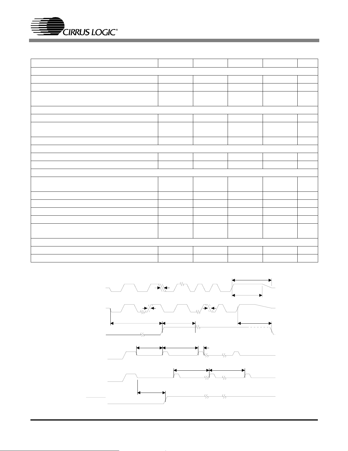
10BASE-T CHARACTERISTICS
Parameter Symbol Min Typ Max Unit
10BASE-T Interface
Transmitter Differential Output Voltage (Peak) V
Receiver Normal Squelch Level (Peak) V
Receiver Low Squelch Level (LoRxSquelch bit
V
OD
ISQ
SQL
set)
10BASE-T Transmitter
TXD Pair Jitter into 100 ΩLoad t
TXD Pair Return to ≤50 mV after Last Positive
TTX1
t
TTX2
Transition
TXD Pair Positive Hold Time at End of Packet t
TTX3
10BASE-T Receiver
Allowable Received Jitter at Bit Cell Center t
Allowable Received Jitter at Bit Cell Boundary t
TRX1
TRX2
10BASE-T Link Integrity
First Transmitted Link Pulse after Last Transmit-
t
LN1
ted Packet
Time Between Transmitted Link Pulses t
Width of Transmitted Link Pulses t
Minimum Received Link Pulses Separation t
Maximum Received Link Pulse Separation t
Last Receive Activity to Link Fail (Link Loss
LN2
LN3
LN4
LN5
t
LN6
Timer)
10Base-T Jabber/Unjabber Timing
Maximum Transmit Time - 105 - ms
Unjabber Time - 406 - ms
2.2 - 2.8 V
300 - 525 mV
125 - 290 mV
--8ns
--4.5µs
250 - - ns
- - +/-13.5 ns
- - +/-13.5 ns
15 16 17 ms
15 16 17 ms
60 - 200 ns
257ms
25 52 150 ms
50 52 150 ms
t
TTX2
TXD±
t
RXD±
Carrier Sense
(Internal)
TXD±
RXD±
LINKLED
t
RTX3
t
RTX1
t
LN1
t
LN6
TTX1
RTX4
t
t
RTX2
t
LN2
t
LN4
t
LN3
t
LN5
t
TTX3
CrystalLAN™ 100BASE-X and 10BASE-T Transceiver 7
Page 8
CS8952
100BASE-X CHARACTERISTICS
Parameter Symbol Min Typ Max Unit
100BASE-TX Transmitter
TX Differential Output Voltage (Peak) V
Signal Amplitude Symmetry V
Signal Rise/Fall Time t
Rise/Fall Symmetry t
Duty Cycle Distortion t
Overshoot/Undershoot t
Transmit Jitter t
TX Differential Output Impedance Z
OP
SYM
RF
RFS
DCD
OS
JT
OUT
100BASE-TX Receiver
Receive Signal Detect Assert Threshold - - 1.0 V
Receive Signal Detect De-assert Threshold 0.2 - - V
Receive Signal Detect Assert Time - - 1000 µs
Receive Signal Detect De-assert Time - - 350 µs
100BASE-FX Transmitter
TX_NRZ+/- Output Voltage - Low V
TX_NRZ+/- Output Voltage - High V
Signal Rise/Fall Time T
1
2
RF
100Base-FX Receiver
RX_NRZ+/- Input Voltage - Low V
RX_NRZ+/- Input Voltage - High V
Common Mode Input Range V
3
4
CMIP
0.95 - 1.05 V
98 - 102 %
3.0 - 5.0 ns
--0.5ns
--+/-0.5ns
--5%
- 400 1400 ps
-100-ohms
-1.830 - -1.605 V
-1.035 - -0.880 V
--1.6ns
-1.830 - -1.605 V
-1.035 - -0.880 V
-3.56-V
p-p
p-p
RX/TX Signaling for 100Base-FX
V
DD
TX_NRZ+/-
V
V
1
2
V
3
RX_NRZ+/-
V
4
0
8 CrystalLAN™ 100BASE-X and 10BASE-T Transceiver
Page 9
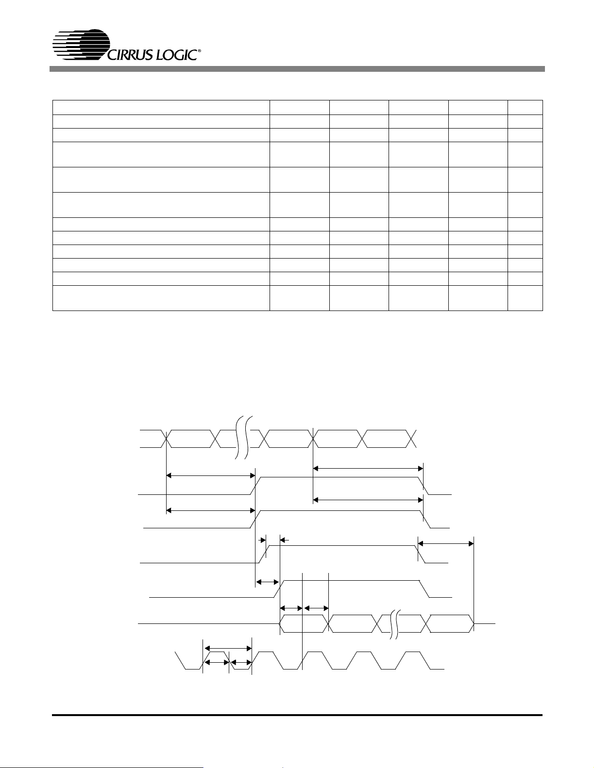
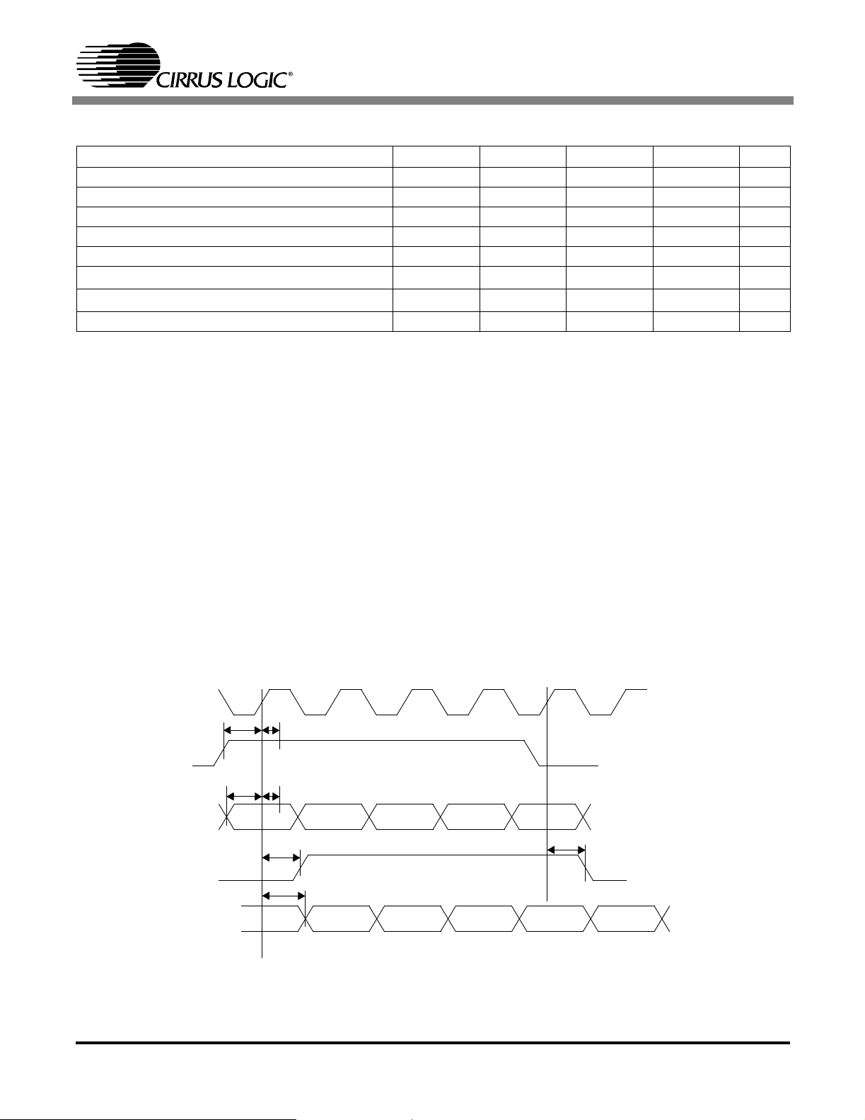
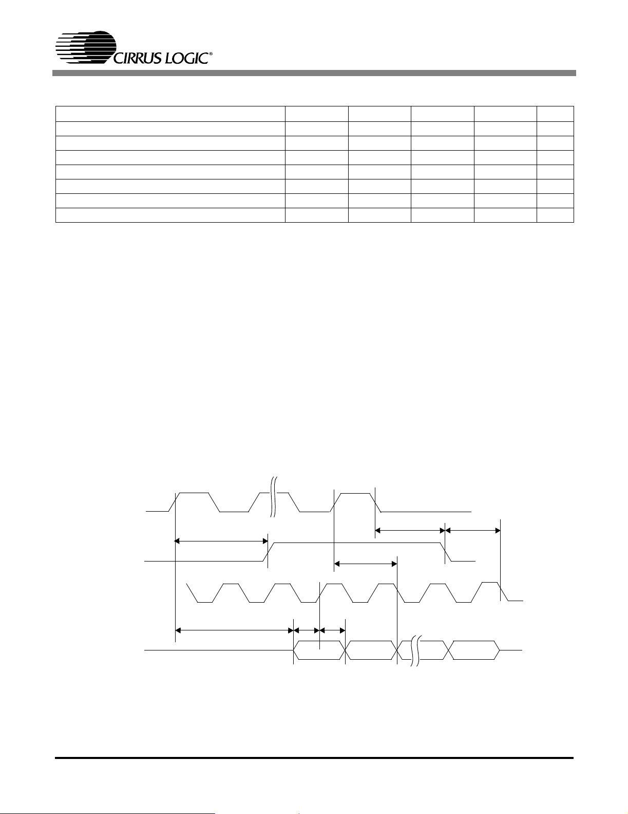
100BASE-TX MII RECEIVE TIMING - 4B/5B ALIGNED MODES
Parameter Symbol Min Typ Max Unit
RX_CLK Period t
RX_CLK Pulse Width t
WL,tWH
RXD[3:0],RX_ER/RXD4,RX_DV setup to rising
edge of RX_CLK
RXD[3:0],RX_ER/RXD4,RX_DV hold from rising
edge of RX_CLK
CRStoRXDlatency 4BAligned
t
5B Aligned
“Start of Stream” to CRS asserted t
“End of Stream” to CRS de-asserted t
“Start of Stream” to COL asserted t
“End of Stream” to COL de-asserted t
CRS1
CRS2
COL1
COL2
RX_EN asserted to RX_DV, RXD[3:0] valid t
RX_EN de-asserted to RX_DV, RXD[3:0].
RX_ER/RXD4 in high impedance state
P
t
SU
t
HD
DLAT
EN
t
DIS
-40-ns
-20-ns
10 - - ns
10 - - ns
2
2
3-6
3-6
-1011BT
--21BT
--11BT
--21BT
-TBD-ns
-TBD-ns
CS8952
8
8
BT
RX+/-
CRS
COL
RX_EN
RX_DV
RXD[3:0],
RX_ER/RXD4
RX_CLK
Start of
Stream
t
CRS1
t
COL1
t
WL
t
RLAT
t
P
t
WH
End of
Stream
t
CRS2
t
COL2
t
EN
t
DIS
t
t
HD
SU
IN
OUT
OUT
IN
OUT
OUT
OUT
CrystalLAN™ 100BASE-X and 10BASE-T Transceiver 9
Page 10
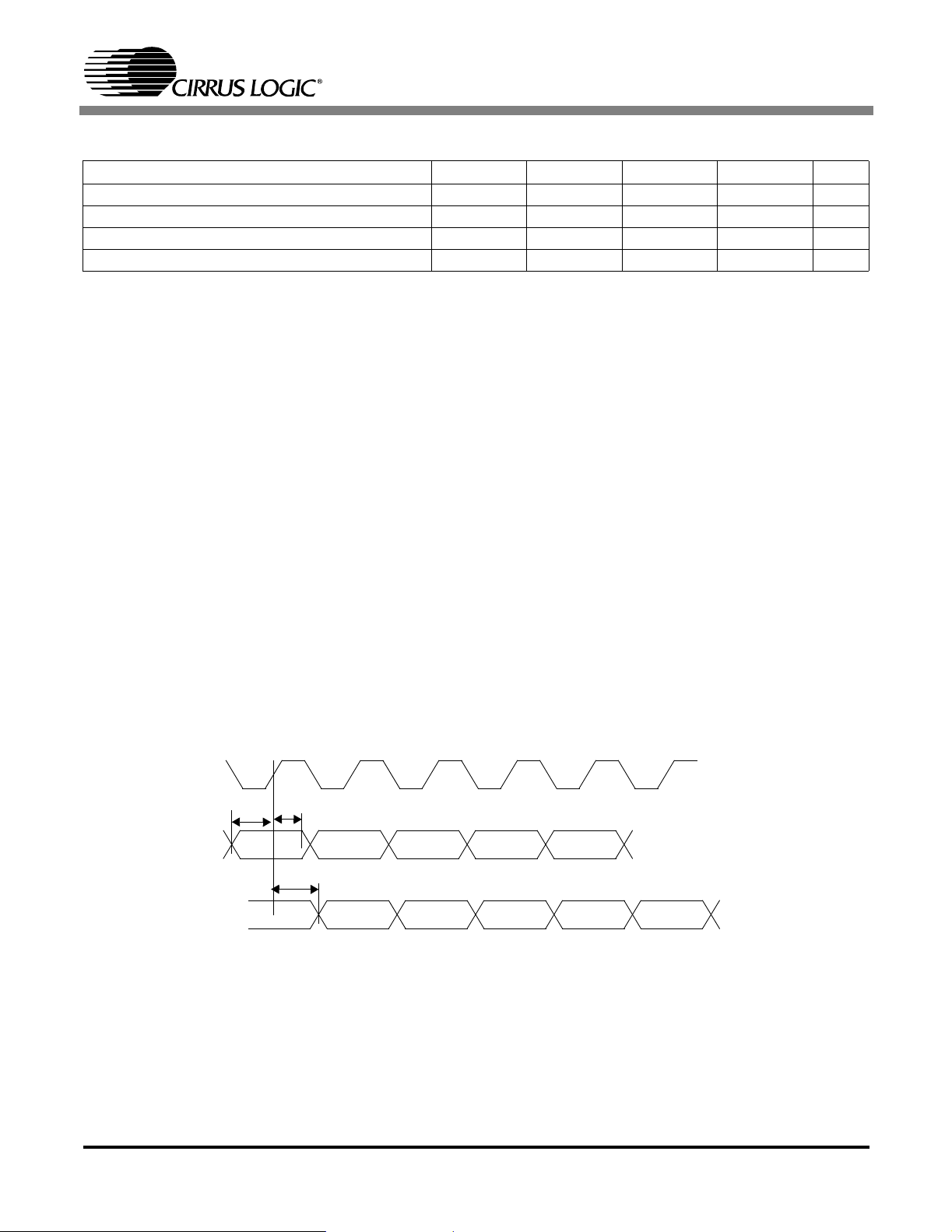
100BASE-TX MII RECEIVE TIMING - 5B BYPASS ALIGN MODE
Parameter Symbol Min Typ Max Unit
RX_CLK Period t
RX_CLK Pulse Width t
WL,tWH
RXD[4:0]setuptorisingedgeofRX_CLK t
RXD[4:0] hold after rising edge of RX_CLK t
Start of 5B symbol to symbol output on RX[4:0]
t
5B Mode
P
SU
HD
RLAT
-40-ns
-20-ns
10 - - ns
10 - - ns
5-9BT
CS8952
RX+/-
RXD[4:0],
RX Symbol
0
t
RLAT
RX Symbol
N-1
t
SU
t
P
t
HD
RX Data
0
RX Symbol
N
RX Data
1
IN
OUT
RX_CLK
OUT
t
t
WL
WH
10 CrystalLAN™ 100BASE-X and 10BASE-T Transceiver
Page 11
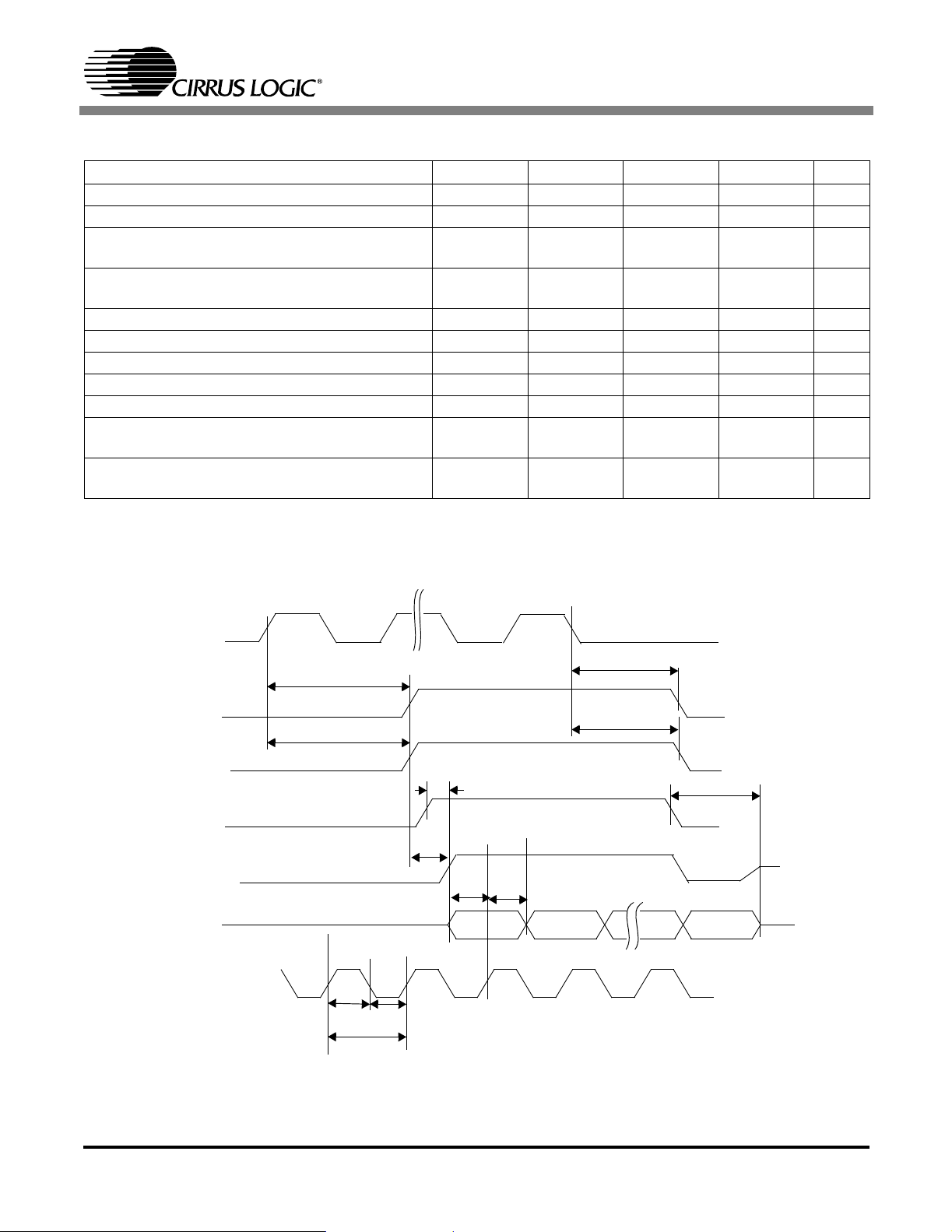
100BASE-TX MII TRANSMIT TIMING - 4B/5B ALIGN MODES
Parameter Symbol Min Typ Max Unit
TXD[3:0] Setup to TX_CLK High t
TX_EN Setup to TX_CLK High t
TXD[3:0] Hold after TX_CLK High t
TX_ER Hold after TX_CLK High t
TX_EN Hold after TX_CLK High t
TX_EN “high” to CRS asserted latency t
TX_EN “low” to CRS de-asserted latency t
TX_EN “high” to TX+/- output (TX Latency) t
SU1
SU2
HD1
HD2
HD3
CRS1
CRS2
LAT
10 - - ns
10 - - ns
0--ns
0--ns
0--ns
-8BT
-8BT
678BT
CS8952
TX_CLK
TX_EN
TXD[3:0],
TX_ER/TXD4
CRS
TX+/-
t
SU2
t
SU1
Data
IN
t
CRS1
t
HD2
t
HD1
t
LAT
Symbol
Out
t
CRS2
Input/Output
Input
Input
Output
Output
CrystalLAN™ 100BASE-X and 10BASE-T Transceiver 11
Page 12
100BASE-TX MII TRANSMIT TIMING - 5B BYPASS ALIGN MODE
Parameter Symbol Min Typ Max Unit
TXD[4:0] Setup to TX_CLK High t
TXD[4:0] Hold after TX_CLK High t
TX_ER Hold after TX_CLK High t
TXD[4:0] Sampled to TX+/- output (TX Latency) t
SU1
HD1
HD2
LAT
10 - - ns
0--ns
0--ns
-67ns
CS8952
TX_CLK
TXD[4:0]
TX+/-
t
SU1
Data
IN
t
LAT
t
HD1
Symbol
OUT
Input/Output
Input
Output
12 CrystalLAN™ 100BASE-X and 10BASE-T Transceiver
Page 13
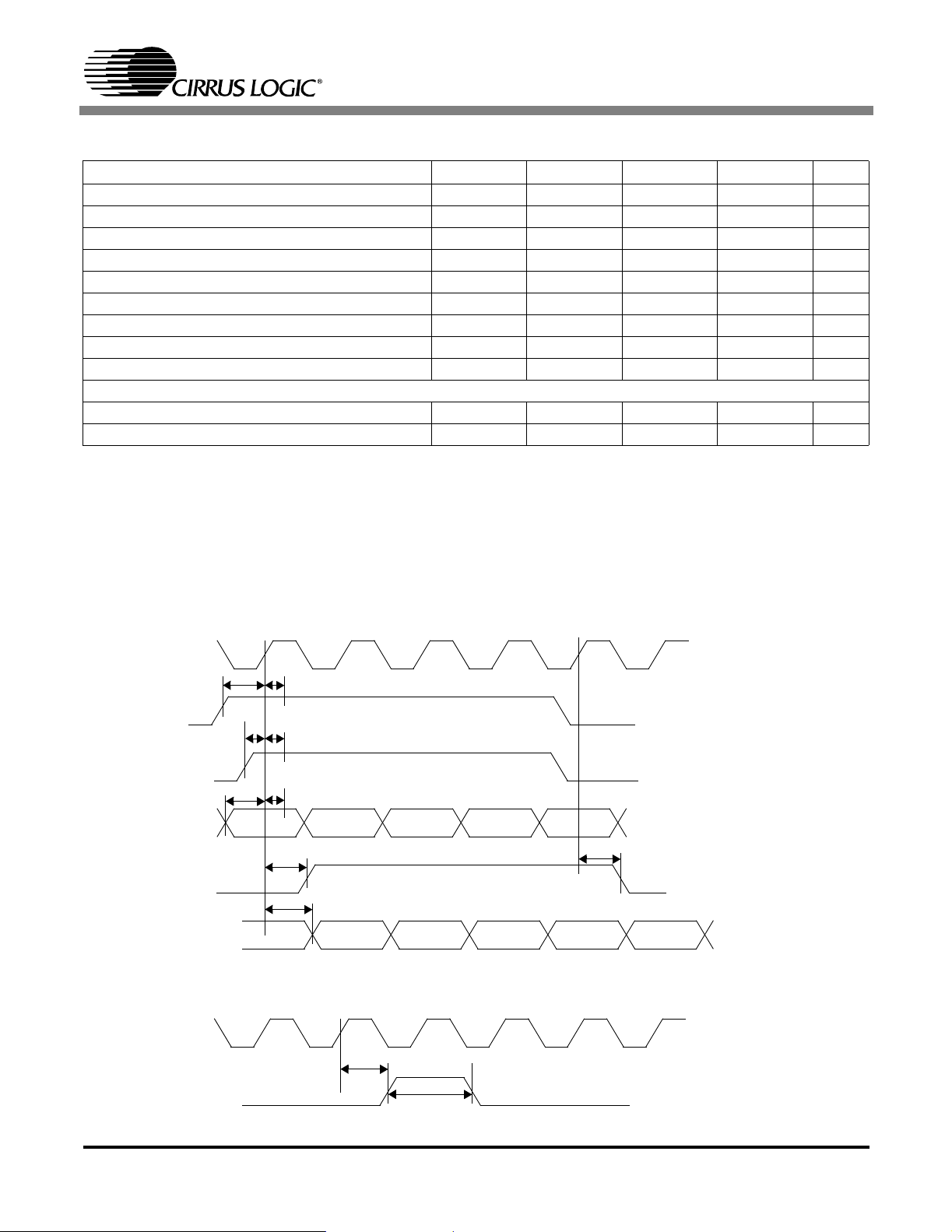
10BASE-T MII RECEIVE TIMING
Parameter Symbol Min Typ Max Unit
RX_CLK Period t
RX_CLK Pulse Width t
RXD[3:0],RX_ER,RX_DVsetuptorisingedgeof
RX_CLK
RXD[3:0], RX_ER, RX_DV hold from rising edge
of RX_CLK
RX data valid from CRS t
RX+/- preamble to CRS asserted t
RX+/- end of packet to CRS de-asserted t
RX+/- preamble to COL asserted t
RX+/- end of packet to COL de-asserted t
RX_EN asserted to RX_DV, RXD[3:0], RX_ER
valid
RX_ENde-assertedto RX_DV, RXD[3:0]. RX_ER
in high impedance state
WL,tWH
P
t
SU
t
HD
RLAT
CRS1
CRS2
COL1
COL2
t
EN
t
DIS
CS8952
-400-ns
-200-ns
30 - - ns
30 - - ns
-810BT
-57BT
2.5 3 BT
0-7BT
--3BT
- - 60 ns
- - 60 ns
RX+/-
CRS
COL
RX_EN
RX_DV
RXD[3:0],
RX_ER
RX_CLK
t
CRS1
t
COL1
t
WL
t
RLAT
t
t
P
WH
IN
t
CRS2
t
COL2
t
EN
t
DIS
t
t
HD
SU
OUT
OUT
IN
OUT
OUT
OUT
CrystalLAN™ 100BASE-X and 10BASE-T Transceiver 13
Page 14
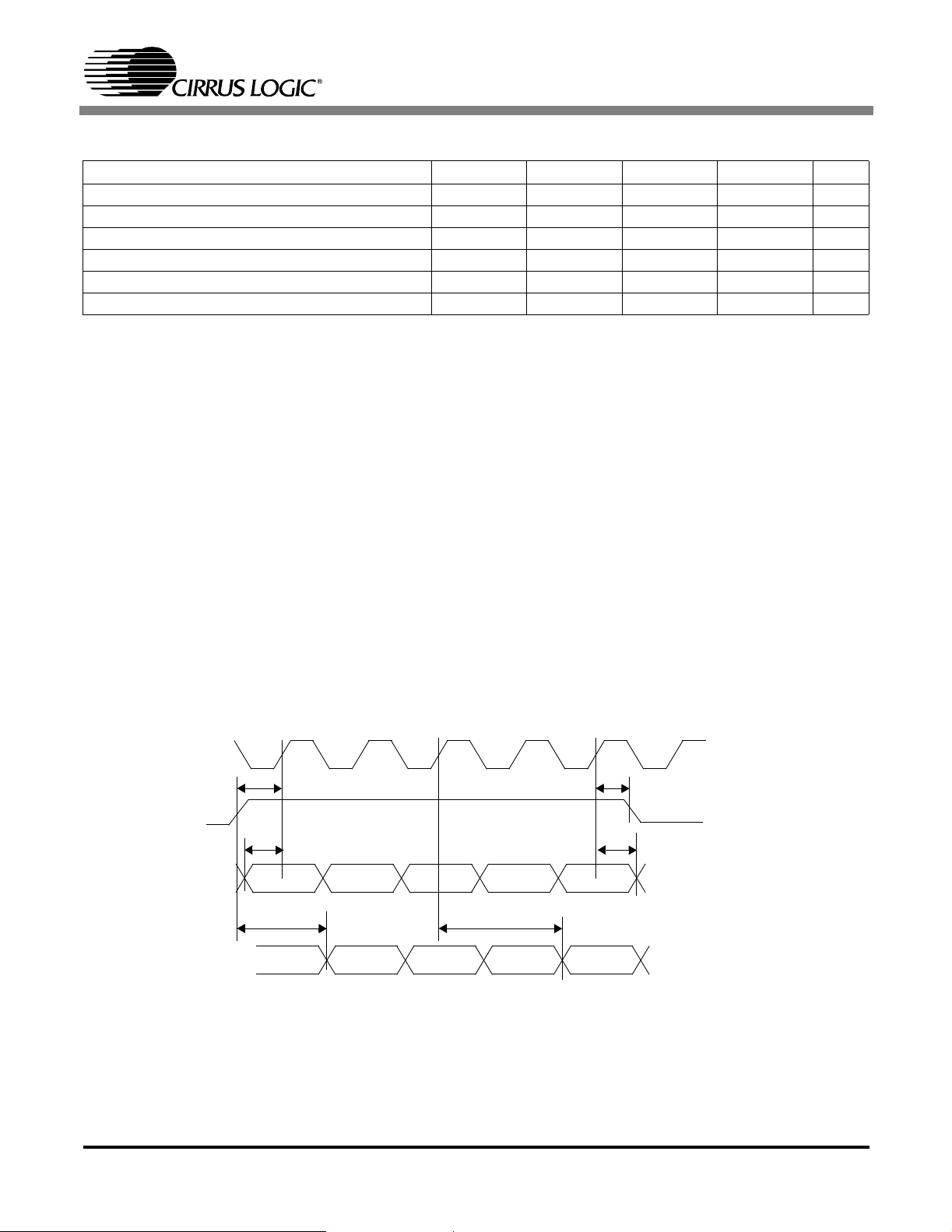
10BASE-T MII TRANSMIT TIMING
Parameter Symbol Min Typ Max Unit
TXD[3:0] Setup to TX_CLK High t
TX_ER Setup to TX_CLK High t
TX_EN Setup to TX_CLK High t
TXD[3:0] Hold after TX_CLK High t
TX_ER Hold after TX_CLK High t
TX_EN Hold after TX_CLK High t
TX_EN “high” to CRS asserted latency t
TX_EN “low” to CRS de-asserted latency t
TX_EN “high” to TX+/- output (TX Latency) t
SQE Timing
COL (SQE) Delay after CRS de-asserted t
COL (SQE) Pulse Duration t
SU1
SU2
SU3
HD1
HD2
HD3
CRS1
CRS2
LAT
COL
COLP
CS8952
10 - - ns
10 - - ns
10 - - ns
0--ns
0--ns
0--ns
0-4BT
0-16BT
6-14BT
0.65 0.9 1.6 µs
0.65 1.0 1.6 µs
TX_CLK
TX_EN
TX_ER
TXD[3:0]
CRS
TX+/-
TX_CLK
t
t
SU3
SU1
t
SU2
t
CRS1
t
t
HD2
t
HD3
HD1
10BASE-T Transmit Timing
t
LAT
Valid
Data
SQE Timing
t
CRS2
Input/Output
Input
Input
Input
Output
Output
Input/Output
t
COL
SQE
t
SQEP
Output
14 CrystalLAN™ 100BASE-X and 10BASE-T Transceiver
Page 15
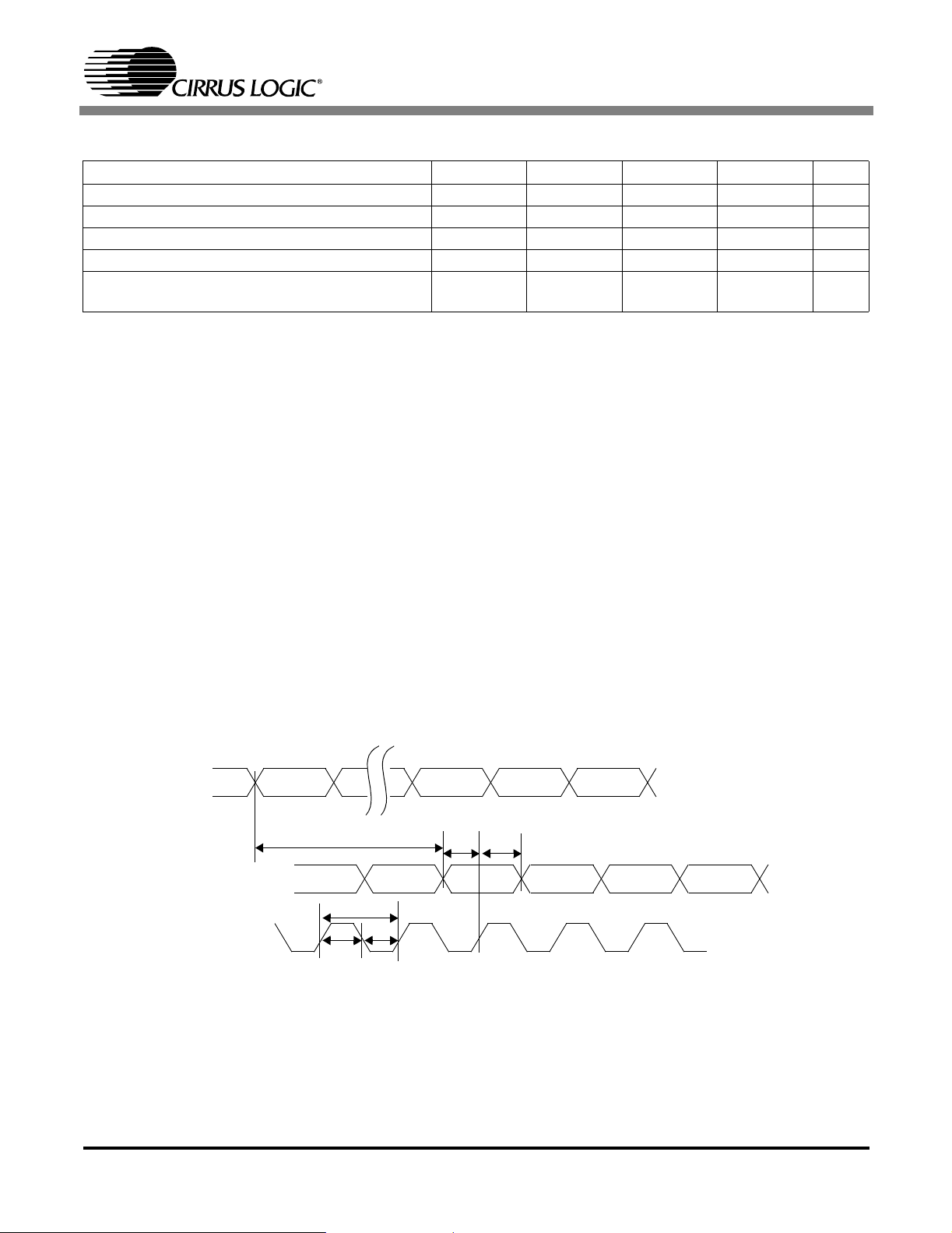
10BASE-T SERIAL RECEIVE TIMING
Parameter Symbol Min Typ Max Unit
RX+/- active to RXD[0] active t
RX+/- active to CRS active t
RXD[0] setup from RX_CLK t
RXD[0] hold from RX_CLK t
RX_CLK hold after CRS off t
RXD[0] throughput delay t
CRS turn off delay t
DATA
CRS
RDS
RDH
RCH
RD
CRSOFF
CS8952
- - 1200 ns
--600ns
35 - - ns
50 - - ns
5--ns
--250ns
--400ns
RX+/-
CRS
t
CRS
t
RD
t
CRSOFF
t
RCH
IN
OUT
RX_CLK
OUT
t
t
HD
SU
OUT
RXD[0]
t
DATA
CrystalLAN™ 100BASE-X and 10BASE-T Transceiver 15
Page 16
10BASE-T SERIAL TRANSMIT TIMING
Parameter Symbol Min Typ Max Unit
TX_EN Setup from TX_CLK t
TX_EN Hold after TX_CLK t
TXD[0] Setup from TX_CLK t
TXD[0] Hold after TX_CLK t
Transmit start-up delay t
Transmit throughput delay t
EHCH
CHEL
DSCH
CHDU
STUD
TPD
CS8952
10 - - ns
10 - - ns
10 - - ns
10 - - ns
--500ns
--500ns
TX_CLK
TX_EN
TXD[3:0]
TX+/-
t
EHCH
t
STUD
t
DSCH
Valid
Data
t
CHEL
t
CHDU
t
PD
Input/Output
Input
Input
Output
16 CrystalLAN™ 100BASE-X and 10BASE-T Transceiver
Page 17

AUTO NEGOTIATION / FAST LINK PULSE TIMING
Parameter Symbol Min Typ Max Unit
FLP burst to FLP burst t
FLP burst width t
Clock/Data pulses per burst
Clock/Data pulse width t
Clock pulse to Data pulse t
Clock pulse to clock pulse t
BTB
FLPW
-
PW
CTD
CTC
15 16 17 ms
-2-ms
17 - 33 ea.
-100-ns
55.5 64 69.5 µs
111 128 139 µs
CS8952
TX+/-
t
FLPW
t
BTB
Clock
Pulse
Data
Pulse
Clock
Pulse
TX+/-
t
t
t
PW
CTD
CTC
t
PW
CrystalLAN™ 100BASE-X and 10BASE-T Transceiver 17
Page 18
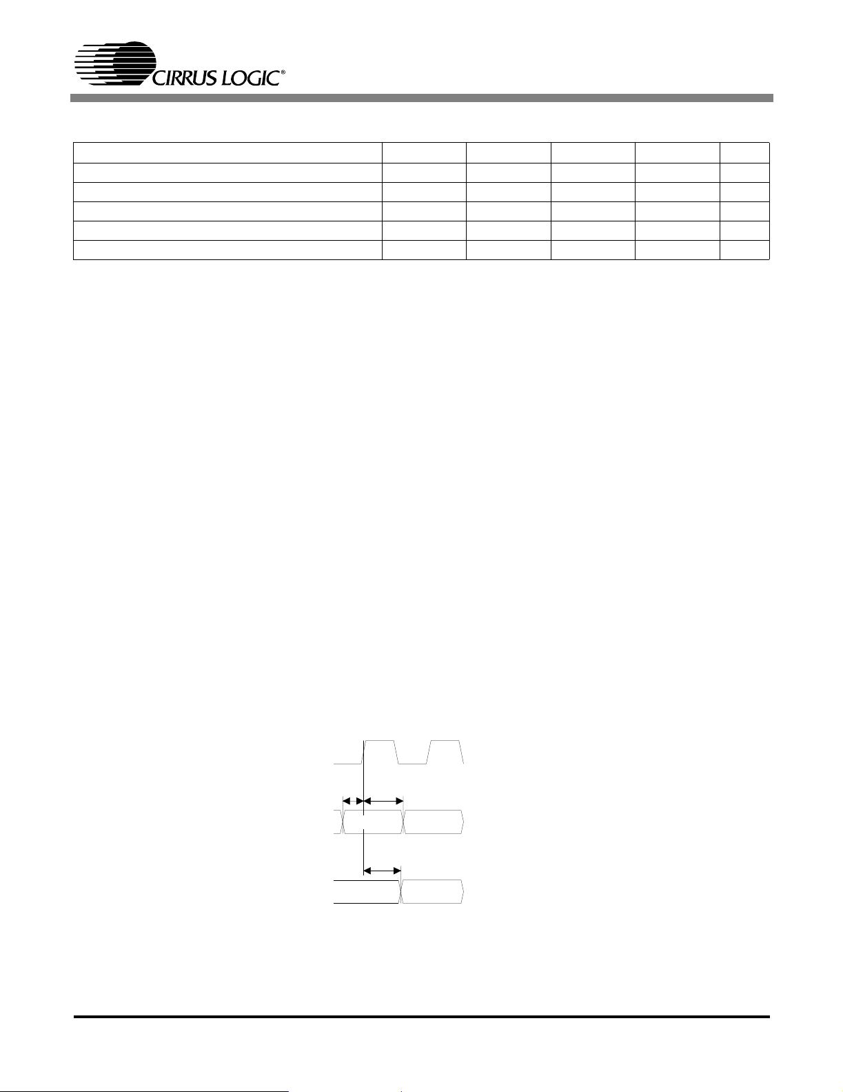
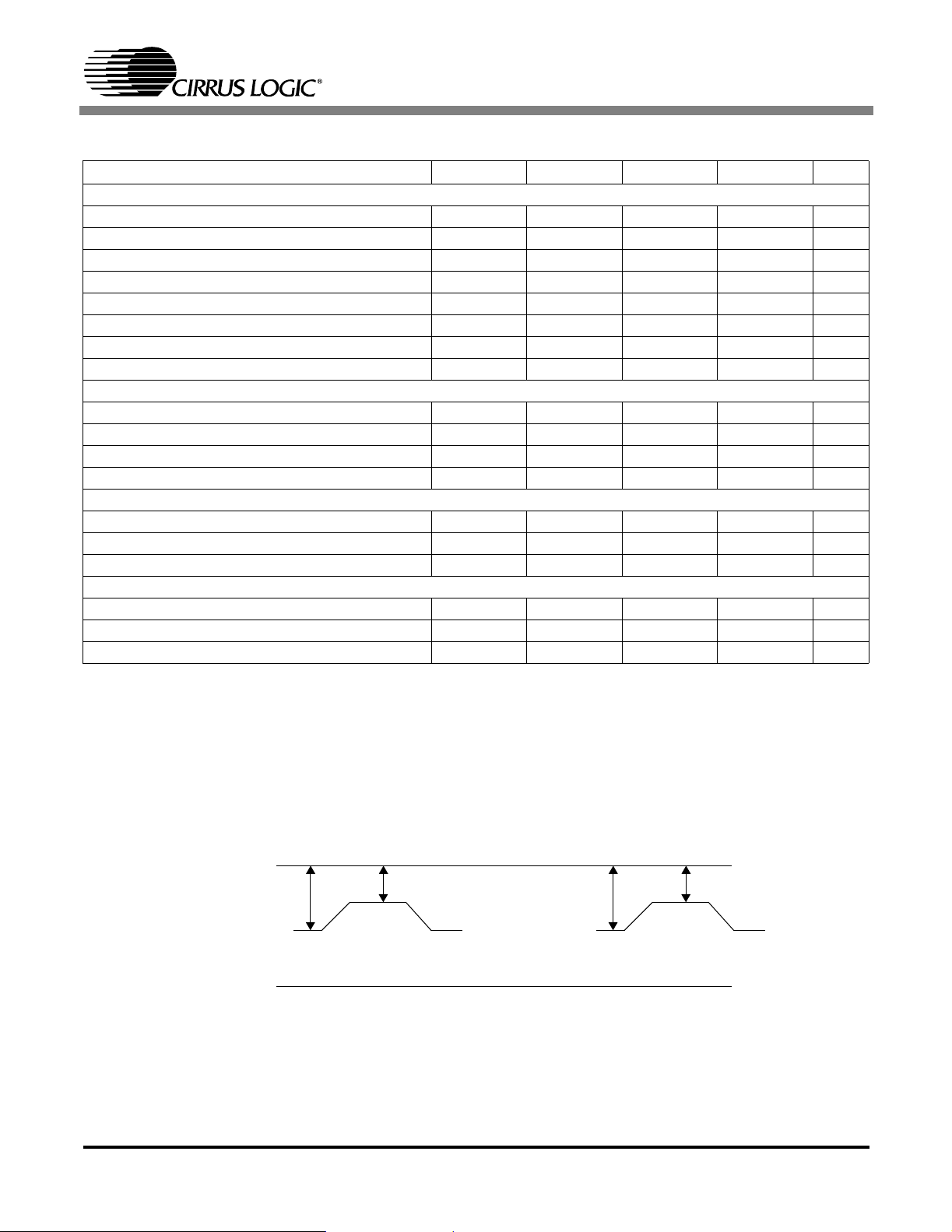
SERIAL MANAGEMENT INTERFACE TIMING
Parameter Symbol Min Typ Max Unit
MDC Period t
MDC Pulse Width t
MDIO Setup to MDC (MDIO as input) t
MDIO Hold after MDC (MDIO as input) t
MDC to MDIO valid (MDIO as output) t
p
WL,tWH
MD1
MD2
MD3
CS8952
60 - - ns
40 - 60 %
10 - - ns
10 - - ns
0 - 40 ns
DIRECTION:
IN or OUT of chip
MDC
MDIO
MDIO
t
MD1tMD2
Valid Data
t
MD3
Valid Data
Valid Data
IN
IN
OUT
18 CrystalLAN™ 100BASE-X and 10BASE-T Transceiver
Page 19

CS8952
2. INTRODUCTION
The CS8952 is a complete physical-layer transceiver for 100BASE-TX and 10BASE-T applications.
Additionally, the CS8952 can be used with an external optical module for 100BASE-FX.
2.1 High Performance Analog
The highly integrated mixed-signal design of the
CS8952 eliminates the need for external analog circuitry such as external transmit or receive filters.
The CS8952 builds upon Cirrus Logic’s experience
in pioneering the high-volume manufacturing of
10BASE-T integrated circuits with “true” internal
filters. The CS8952, CS8920, CS8904, and
CS8900 include fifth-order, continuous-time Butterworth 10BASE-T transmit and receive filters, allowing those products to meet 10BASE-T wave
shape, emission, and frequency content requirements without external filters.
2.2 Low Power Consumption
The CS8952 is implemented in low power CMOS,
consuming only 135 mA typically. Three low-power modes are provided to make the CS8952 ideal
for power sensitive applications such as CardBus.
2.3 Application Flexibility
The CS8952’s digital interface and operating
modes can be tailored to efficiently support a wide
variety of applications. For example, the Media Independent Interface (MII) supports 100BASE-TX,
100BASE-FX and 10BASE-T NIC cards, switch
ports and router ports. Additionally, the low-latency “repeater” interface mode minimizes data delay
through the CS8952, facilitating system compliance with overall network delay budgets. To support 10BASE-T applications, the CS8952 provides
a 10BASE-T serial port (Seven-wire ENDEC interface).
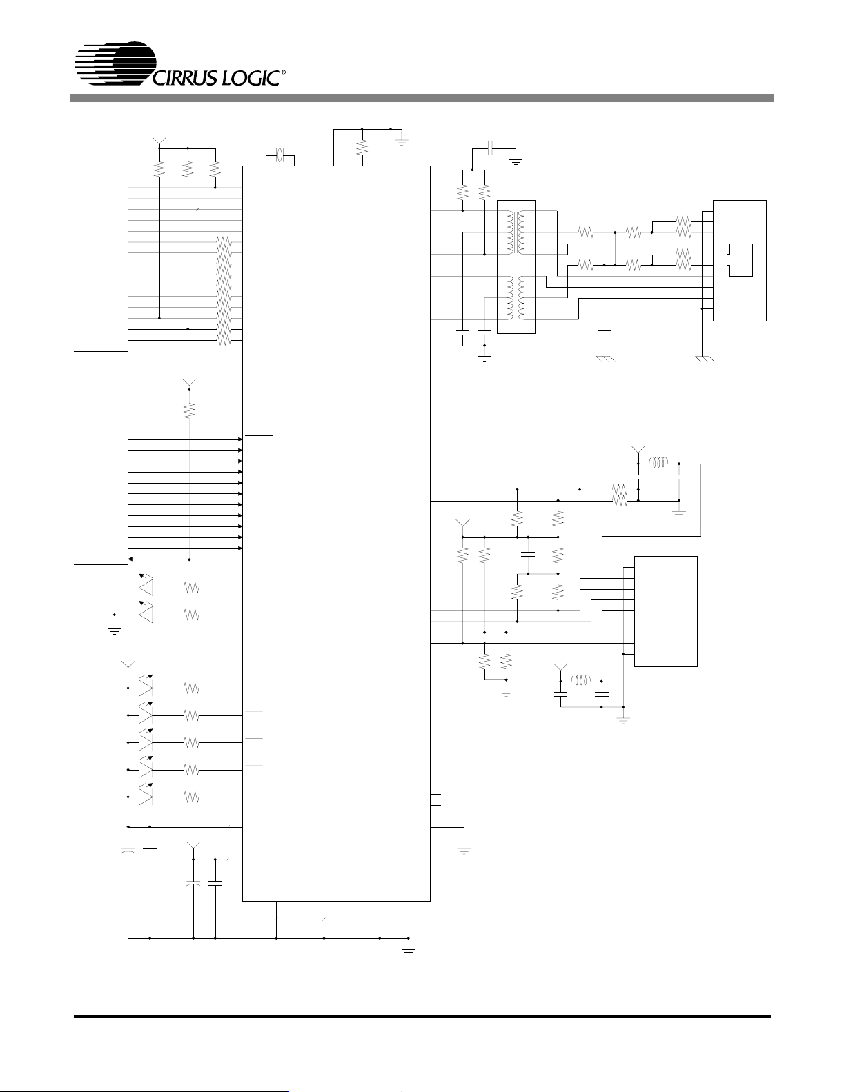
2.4 Typical Connection Diagram
Figure 1 illustrates a typical MII to CS8952 appli-
cation with twisted-pair and fiber interfaces. Refer
to the Analog Design Considerations section for
detailed information on power supply requirements
and decoupling, crystal and magnetics requirements, and twisted-pair and fiber transceiver connections.
3. FUNCTIONAL DESCRIPTION
The CS8952is a complete physical-layer transceiver for 100BASE-TX and 10BASE-T applications.
It provides a Physical Coding Sub-layer for communication with an external MAC (Media Access
Controller). The CS8952 also includes a complete
Physical Medium Attachment layer and a
100BASE-TX and 10BASE-T Physical Medium
Dependent layer. Additionally, the CS8952 provides a PECL interface to an external optical module for 100BASE-FX applications.
The primary digital interface to the CS8952 is an
enhanced IEEE 802.3 Media Independent Interface
(MII). The MII supports parallel data transfer, access to the CS8952 Control and Status registers,
and several status and control pins. The CS8952's
operating modes can be tailored to support a wide
variety of applications, including low-latency
100BASE-TX repeaters, switches and MII-based
network interface cards.
For 100BASE-TX applications, the digital data interface can be either 4-bit parallel (nibbles) or 5-bit
parallel (code-groups). For 10BASE-T applications, the digital data format can be either 4-bit parallel (nibbles) or one-bit serial.
The CS8952 is controlled primarily by configuration registers via the MII Management Interface.
Additionally, a number of the most fundamental
register bits can be set at power-up and reset time
by connecting pull-up or pull-down resistors to external pins.
The CS8952's MII interface is enhanced beyond
IEEE requirements by register extensions and the
addition of pins for MII_IRQ
DEF signals. The MII_IRQ
,RX_EN,andISO-
pin provides an inter-
CrystalLAN™ 100BASE-X and 10BASE-T Transceiver 19
Page 20
CS8952
MII
I/F
CONTROL
I/F
10 µF 0.1µF
VDD_MII
VDD_MII
4.7 k
1.5 k
4.7 k
Ω
Ω
4
Ω
33
33
Ω
33
Ω
33
Ω
33
Ω
33
Ω
Ω
33
Ω
33
Ω
33
33
Ω
VDD_MII
4.7 k
Ω
680
Ω
680
680
Ω
680
Ω
Ω
680
680
Ω
Ω
680
+5 V
10 µF 0.1 µF
25 MHz
Ω
XTAL_I XTAL_O
MDIO
MDC
TXD
TX_ER/TXD[4]
TX_EN
TX_CLK
RX_CLK
RXD[0]
RXD[1]/PHYAD[1]
RXD[2]
RXD[3]/PHYAD[3]
RX_ER/RXD[4]/PHYAD[4]
RX_DV/MII_DRV
COL/PHYAD0
CRS/PHYAD[2]
LPSTRT
RX_EN
PWRDN
REPEATER
BPSCR
BP4B5B
BPALIGN
LPBK
ISODEF
10BT_SER
RESET
MII_IRQ
SPEED10
SPEED100
LED1
LED2
LED3
LED4
LED5
3
VDD_MII
11
VDD
RSVD VSS TEST0 TEST1
7 21
VSS18 RES VSS17
CS8952
4.99 k
Ω
49.9
RX+
RX-
TX+
TX-
0.1 µF 0.1 µF
SIGNAL+
SIGNAL-
82
TX_NRZTX_NRZ+
RX_NRZ-
RX_NRZ+
TXSLEW0
TXSLEW1NCNC
AN0
AN1NCNC
TCM
Ω
+5 V
Ω
130
0.1 µF
49.9
82
82
49.9Ω49.9
Ω
Ω
Ω
0.1 µF
Ω
130
68
Ω
Ω
63.4
Ω
+5 V
Ω
0.1 µF 0.1 µF
51
Ω
0.01 µF
2KV
0.1 µF
Ω
Ω
Ω
51
51
Ω
+5 V
TRANSCEIVER
VEE
SD+
TDTD+
VCC
VCC
RDRD+
VEE
51
51
51
0.1 µF
FIBER
Ω
Ω
Ω
Ω
75
75
Ω
130
191
SHLD
8
7
6
5
4
3
2
1
SHLD
RJ45
Figure 1. Typical Connection Diagram
20 CrystalLAN™ 100BASE-X and 10BASE-T Transceiver
Page 21
CS8952
rupt signal to the controller when a change of state
has occurred in the CS8952, eliminating the need
for the system to poll the CS8952 for state changes.
The RX_EN signal allows the receiver outputs to
be electrically isolated. The ISODEF pin controls
the value of register bit ISOLATE in the Basic
Mode Control Register (address 00h) which in turn
electrically isolates the CS8952's MII data path.
3.1 Major Operating Modes
The following sections describe the four major operating modes of the CS8952:
- 100BASE-X MII Modes (TX and FX)
- 100BASE-X Repeater Modes
- 10BASE-T MII Mode
- 10BASE-T Serial Mode
The choice of operating speed (10 Mb/s versus
100 Mb/s) is made using the auto-negotiation input
pins (AN0, AN1) and/or the auto-negotiation MII
registers. The auto-negotiation capability also is
used to select a duplex mode (full or half duplex).
Both speed and duplex modes can either be forced
or negotiated with the far-end link partner.
The digital interface mode (MII, repeater, or
10BASE-T serial) is selected by input pins
BPALIGN, BP4B5B and 10BT_SER as shown in
Table 1. Speed and duplex selection are made
through the AN[1:0] pins as shown in Table 5.
Operating Mode BPALIGN BP4B5B 10BT_SER
100BASE-X MII 0 0 0
10BASE-T MII 0 0 0
Table 1.
Operating Mode BPALIGN BP4B5B 10BT_SER
100BASE-X
Repeater
10BASE-T Serial Don’t
1Don’t
Care
01 0
Don’t
Care
Table 1.
Care
0
1
3.1.1 100BASE-X MII Application (TX and FX)
The CS8952 provides an IEEE 802.3-compliant
MII interface. Data is transferred across the MII in
four-bit parallel (nibble) mode. TX_CLK and
RX_CLK are nominally 25 MHz for 100BASE-X.
The 100BASE-X mode includes both the TX and
FX modes, as determined by pin BPSCR (bypass
scrambler), or the BPSCR bit (bit 13) in the Loopback, Bypass, and Receiver Error Mask Register
(address 18h). In FX mode, an external optical
module is connected to the CS8952 via pins
TX_NRZ+, TX_NRZ-, RX_NRZ+, RX_NRZ-,
SIGNAL+, and SIGNAL-. In FX mode, the MLT3/NRZI conversion blocks and the scrambler/descrambler are bypassed.
3.1.1.1 Symbol Encoding and Decoding
In 100BASE-X modes, 4-bit nibble transmit data is
encoded into 5-bit symbols for transmission onto
the media as shown in Tables 2 and 3. The encoding is necessary to allow data and control symbols
to be sent consecutively along the same media
transparent to the MAC layer. This encoding causes the symbol rate transmitted across the wire (125
symbols/second) to be greater than the actual data
rate of the system (100 symbols/second).
DATA and CONTROL Codes (RX_ER = 0 or TX_ER = 0)
Name 5-bit Symbol 4-bit Nibble Comments
DATA (Note 1)
0 11110 0000
1 01001 0001
CrystalLAN™ 100BASE-X and 10BASE-T Transceiver 21
Page 22
DATA and CONTROL Codes (RX_ER = 0 or TX_ER = 0)
Name 5-bit Symbol 4-bit Nibble Comments
2 10100 0010
3 10101 001 1
4 01010 0100
5 01011 0101
6 01110 0110
7 01111 0111
8 10010 1000
9 10011 1001
A 10110 1010
B 10111 1011
C 11010 1100
D 11011 1101
E 11100 1110
F 11101 1111
CONTROL (Note 2)
I 11111 0101 IDLE (Note 3)
J 11000 0101 First Start of Stream Symbol
K 10001 0101 Second Start of Stream Symbol
T 01101 0000 First End of Stream Symbol
R 00111 0000 Second End of Stream Symbol
1. DATA code groups are indicated by RX_DV = 1
2. CONTROL code groups areinserted automatically during transmission in response to
TX_EN. They are not generated through any combination of TXD[3:0] or TX_ER.
3. IDLE is indicated by RX_DV = 0.
Table 2. 4B5B Symbol Encoding/Decoding
CS8952
Code Violations (RX_ER = 1 or TX_ER = 1)
Error Report
Normal Mode 4-bit
Name 5-bit Symbol
CONTROL (Note 1)
I 11111 0000 0000 This portion of the table relates received
J 11000 0000 0000
K 10001 0000 0000
T 01101 0000 0000
R 00111 0000 0000
CODE VIOLATIONS
H 00100 0000 0000
V0 00000 0110 or 0101 (Note 2) 0001
V1 00001 0110 or 0101 (Note 2) 0111
V2 00010 0110 or 0101 (Note 2) 1000
V3 00011 0110 or 0101 (Note 2) 1001
V4 00101 0110 or 0101 (Note 2) 1010
V5 00110 0110 or 0101 (Note 2)1011
22 CrystalLAN™ 100BASE-X and 10BASE-T Transceiver
Nibble
Mode 4-bit
Nibble Comments
5-bit symbols to received 4-bit nibbles
only . The control code groups may not
be transmitted in the data portion of the
frame.
Page 23
Code Violations (RX_ER = 1 or TX_ER = 1)
Error Report
Normal Mode 4-bit
Name 5-bit Symbol
V6 01000 0110 or 0101 (Note 2)1100
V7 01100 0110 or 0101 (Note 2)1101
V8 10000 0110 or 0101 (Note 2)1110
V9 11001 0110 or 0101 (Note 2) 1111
1. CONTROL code groups become violations when found in the data portion of the frame.
2. Invalid code groups are mapped to 5h unless the Code Error Report select bit in the Loopback,
Bypass,and Receiver Error Mask Register(address 18h) is set, in which case invalid code groupsare
mapped to 6h.
Nibble
Table3. 4B5BCodeViolationDecoding
Mode 4-bit
Nibble Comments
CS8952
3.1.1.2 100 Mb/s Loopback
One of two internal 100BASE-TX loopback modes
can be selected. Local loopback redirects the
TXD[3:0] input data to RXD[3:0] data outputs
through the 4B5B coders and scramblers. Local
loopback is selected by asserting pin LPBK, by setting the LPBK bit (bit 14) in the Basic Mode Control Register (address 00h) or by setting bits 8 and
11 in the Loopback, Bypass, and Receiver Error
Mask Register (address 18h) as shown in Table 4.
Remote loopback redirects the analog line interface
inputs to the analog line driver outputs. Remote
loopback is selected by setting bit 9 in the Loopback, Bypass, and Receiver Error Mask Register
(address 18h) as shown in Table 4.
Remote
Loopback
(bit 9)
0 0 No Loopback
0 1 Local Loopback (toward MII)
1 0 Remote Loopback (toward line)
1 1 Operation is undefined
When changing between local and non-loopback
modes, the data on RXD[3:0] will be undefined for
approximately 330 µs.
PMD
Loopback
(bit 8)
Function
Table 4.
3.1.2 100BASE-X Repeater Application
The CS8952 provides two low latency modes for
repeater applications. These are selected by asserting either pin BPALIGN or BP4B5B. Both pins
have the effect of bypassing the 4B5B encoder and
decoder. Bypassing the coders decreases latency,
and uses a 5-bit wide parallel code group interface
on pins RXD[4:0] and TXD[4:0] instead of the 4bit wide MII nibble interface on pins RXD[3:0] and
TXD[3:0]. In repeater mode, pin RX_ER is redefined as the fifth receive data bit (RXD4), and pin
TX_ER is redefined as the fifth transmit data bit
(TXD4).
BPALIGN can also be selected by setting bit 12 in
Loopback, Bypass, and Receiver Error Mask Register (address 18h). BP4B5B can be selected by setting bit 14 of the same register.
Pin BPALIGN causes more of the CS8952 to be
bypassed than the BP4B5B pin. BPALIGN also bypasses the scrambler/descrambler, and the NRZI to
NRZ converters (see Figure 1). Also, for repeater
applications, pin REPEATER should be asserted to
redefine the function of the CRS (carrier sense) pin.
The REPEATER function may also be invoked by
setting bit 12 in the PCS Sublayer Configuration
Register (address 17h).
For repeater applications, the RX_EN pin can be
used to gate the receive data pins (RXD[4:0],
CrystalLAN™ 100BASE-X and 10BASE-T Transceiver 23
Page 24

CS8952
RX_CLK, RX_DV, COL, and CRS) onto a shared,
external repeater system bus.
3.1.3 10BASE-T MII Application
The digital interface used in this mode is the same
as that used in the 100BASE-X MII mode except
that TX_CLK and RX_CLK are nominally
2.5 MHz.
The CS8952 includes a full-featured 10BASE-T in-
terface, as described in the following sections.
3.1.3.1 Full and Half Duplex operation
The 10BASE-T function supports full and half duplex operation as determined by pins AN[1:0]
and/or the corresponding MII register bits. (See Table 5).
3.1.3.2 Collision Detection
If half duplex operation is selected, the CS8952 detects a 10BASE-T collision whenever the receiver
and transmitter are active simultaneously. When a
collision is present, the collision is reported on pin
COL. Collision detection is undefined for full-duplex operation.
3.1.3.3 Jabber
The jabber timer monitors the transmitter and disables the transmissionif the transmitter is active for
greaterthan approximately 105 ms. The transmitter
stays disabled until approximately 406 ms after the
internal transmit request is no longer enabled.
3.1.3.4 Link Pulses
To prevent disruption of network operation due to a
faulty link segment, the CS8952 continually monitors the 10BASE-T receive pair (RXD+ and RXD-)
for packets and link pulses. After each packet or link
pulse is received, an internal Link-Loss timer is
started. As long as a packet or link pulse is received
before the Link-Loss timer finishes (between 50 and
100 ms), the CS8952 maintains normal operation. If
no receive activity is detected, the CS8952 disables
packet transmission to prevent “blind” transmissions onto the network (link pulses are still sent
while packet transmission is disabled). To reactivate
transmission, the receiver must detect a single packet (the packet itself is ignored), or two normal link
pulses separated by more than 6 ms and no more
than 50 ms.
The CS8952 automatically checks the polarity of
the receive half of the twisted pair cable. To detect
a reversed pair, the receiver examines received link
pulses and the End-of-Frame (EOF) sequence of
incoming packets. If it detects at least one reversed
link pulse and at least four frames in a row with
negative polarity after the EOF, the receive pair is
considered reversed. If the polarity is reversed and
bit 1 of the 10BASE-T Configuration Register (address 1Ch), is set, the CS8952 automatically corrects a reversal.
In the absence of transmit packets, the transmitter
generates link pulses in accordance with
Section 14.2.1.1 of the Ethernet standard. Transmitted link pulses are positive pulses, one bit time
wide, typically generated at a rate of one every
16 ms. The 16 ms timer also starts whenever the
transmitter completes an End-of-Frame (EOF) sequence. Thus, a link pulse will be generated 16 ms
after an EOF unless there is another transmitted
packet.
3.1.3.5 Receiver Squelch
The 10BASE-T squelch circuit determines when
valid data is present on the RXD+/RXD- pair. Incoming signals passing through the receive filter
are tested by the squelch circuit. Any signal with
amplitude less than the squelch threshold (either
positive or negative, depending on polarity) is rejected.
3.1.3.6 10BASE-T Loopback
When Loopback is selected, the TXD[3:0] pins are
looped back into the RXD[3:0] pins through the
24 CrystalLAN™ 100BASE-X and 10BASE-T Transceiver
Page 25

CS8952
Manchester Encoder and Decoder. Selection is
made via:
- setting bit 14 in the Basic Mode Control
Register (address 00h) or
- setting bits 8 and 11 in the Loopback, Bypass, and Receiver Error Mask Register
(address 18h) or
- asserting the LPBK pin.
3.1.3.7 Carrier Detection
The carrier detect circuit informs the MAC that valid receive data is present by asserting the Carrier
Sense signal (CRS) as soon it detects a valid bit pattern (1010b or 0101b for 10BASE-T). During normal packet reception, CRS remains asserted while
the frame is being received, and is de-asserted
within 2.3 bit times after the last low-to-high transition of the End-of-Frame (EOF) sequence. Whenever the receiver is idle (no receive activity), CRS
is de-asserted.
3.1.4 10BASE-T Serial Application
This mode is selected when pin 10BT_SERis asserted during power-up or reset, and operates similar to the 10BASE_T MII mode except that data is
transferred serially on pins RXD0 and TXD0 using
a10MHzRX_CLKandTX_CLK.Receivedatais
framed by CRS rather than RX_DV.
3.2 Auto-Negotiation
The CS8952 supports auto-negotiation, which is
the mechanism that allows the two devices on either end of an Ethernet link segment to share information and automatically configure both devices
for maximum performance. When configured for
auto-negotiation, the CS8952 will detect and automatically operate full-duplex at 100 Mb/s if the device on the other end of the link segment also
supports full-duplex, 100 Mb/s operation, and
auto-negotiation. The CS8952 auto-negotiation capability is fully compliant with the relevant portions of section 28 of the IEEE 802.3u standard.
The CS8952 can auto-negotiate both operating
speed (10 versus 100 Mb/s), duplex mode (half duplex versus full duplex), and flow control (pause
frames), or alternatively can be set not to negotiate.
At power-up and reset times, the auto-negotiation
mode is selected via the auto-negotiation input pins
(AN[1:0]). This selection can later be changed using the Auto-Negotiation Advertisement Register
(address 04h).
Pins AN[1:0] are three level inputs, and have the
function shown in Table 5.
CrystalLAN™ 100BASE-X and 10BASE-T Transceiver 25
Page 26

AN1 AN0 Forced/
Auto
Low Floating Forced 10 Half
High Floating Forced 10 Full
Floating Low Forced 100 Half
Floating High Forced 100 Full
Floating Floating Auto-Neg 100/10 Full/Half
Low Low Auto-Neg 10 Half
Low High Auto-Neg 10 Full
High Low Auto-Neg 100 Half
High High Auto-Neg 100 Full
Table 5.
Speed
(Mb/s)
Full/Half
Duplex
Auto-Negotiation encapsulates information within
a burst of closely spaced Link Integrity Test Pulses,
referred to as a Fast Link Pulse (FLP) Burst. The
FLP Burst consists of a series of Link Integrity
Pulses which form an alternating clock / data sequence. Extraction of the data bits from the FLP
Burst yields a Link Code Word which identifies the
capability of the remote device.
CS8952
SET bit (bit 15 of the Basic Mode Control Register (address 00h)) is set.
4) Digital circuitry is reset whenever bit 0 of the
PCS Sub-Layer Configuration Register (address 17h) is set. Analog circuitry is unaffected.
5) Analog circuitry is reset and recalibrated whenever the CS8952 enters or exits the powerdown state, as requested by pin PWRDN.
6) Analog circuitry is reset and recalibrated whenever the CS8952 changes between 10 Mb/s and
100 Mb/s modes.
After a reset, the CS8952 latches the signals on various input pins in order to initialize key registers
and goes through a self configuration. This includes calibrating on-chip analog circuitry. Time
required for t he reset calibration is typically 40 ms.
External circuitry may access registers internal to
the CS8952 during this time. Reset and calibration
complete is indicated when bit 15 of the Basic
Mode Control Register (address 00h) is clear.
In order to support legacy 10 and 100 Mb/s devices, the CS8952 also supports parallel detection. In
parallel detection, the CS8952 monitors activity on
the media to determine the capability of the link
partner even without auto-negotiation having occurred.
3.3 Reset Operation
Resetoccurs in responseto six differentconditions:
1) There is a chip-wide reset whenever the RESET pin is high for at least 200 ns. During a
chip-wide reset, all circuitry and registers in the
CS8952 are reset.
2) When power is applied, the CS8952 maintains
reset until the voltage at the VDD supply pins
reaches approximately 3.6 V. The CS8952
comes out of reset once VDD is greater than approximately 3.6 V and the crystal oscillator has
stabilized.
3.4 LED Indicators
The LEDx, SPD100, and SPD10 output pins provide status information that can be used to drive
LEDs or can be used as inputs to external control
circuitry. Indication options include: receive activity, transmit activity, collision, carrier sense, polarity OK, descrambler synchronization status, autonegotiation status, speed (10 vs. 100), and duplex
mode.
4. MEDIA INDEPENDENT INTERFACE (MII)
The Media Independent Interface (MII) provides a
simple interconnect to an external Media Access
Controller (MAC). This connection may be chip to
chip, motherboard to daughterboard, or a connection between two assemblies attached by a limited
length of shielded cable and an appropriate connector.
3) There is a chip-wide reset whenever the RE-
26 CrystalLAN™ 100BASE-X and 10BASE-T Transceiver
The MII interface uses the following pins:
Page 27

CS8952
STATUS Pins
- COL - Collision indication, valid only for
half duplex modes.
- CRS - Carrier Sense indication
SERIAL MANAGEMENT Pins
- MDIO - a bi-directional serial data path
- MDC - clock for MDIO (16.7 MHz max)
- MII_IRQ
- Interrupt indicating change in
the Interrupt Status Register (address 11h)
RECEIVE DATA Pins
- RXD[3:0] - Parallel data output path
- RX_CLK - Recovered clock output
- RX_DV - Indicates when receive data is
present and valid
- RX_ER - Indicates presence of error in received data
- RX_EN - Can be used to tri-state receiver
output pins
TRANSMIT DATA Pins
- TXD[3:0] - Parallel data input path
- TX_CLK - Transmit clock
- TX_EN - Indicates when transmit data is
present and valid
- TX_ER - Request to transmit a 100BASET HALT symbol, ignored for 10BASE-T
operation.
The interface uses TTL signal levels, which are
compatible with devices operating at a nominal
supply voltage of either 5.0 or 3.3 volts. It is capable of supporting either 10 Mb/s or 100 Mb/s data
rates transparently. That is, all signaling remains
identical at either data rate; only the nominal clock
frequency is changed.
4.1 MII Frame Structure
Data frames transmitted through the M II have the
following format:
Preamble
(7 Bytes)
Start of
Frame
Delimiter
(1 Byte)
Data End of
Frame
Delimiter
Each frame is preceded by an inter-frame gap. The
inter-frame gap is an unspecified time during
which no data activity occurs on the media as indicated by the de-assertion of CRS for the receive
path and TX_EN for the transmit path.
The Preamble consists of seven bytes of 10101010.
The Start of Frame Delimiter consists of a single
byte of 10101011.
Data may be any number of bytes.
The End of Frame Delimiter is conveyed by the de-
assertion of RX_DV and TX_EN for receive and
transmit paths, respectively.
Transmission and/or reception of each byte of data
is done one nibble at a time in the following order:
First Bit
MII
Nibble
Stream
MSB
LSB MSB
First Second
LSB
D0
D1
D2
D3
MAC’s Serial Bit Stream
D0
D1 D2 D3 D4 D5 D6 D7
NibbleNibble
4.2 MII Receive Data
The presence of recovered data on the RXD[3:0]
bus is indicated by the assertion of RX_DV.
RX_DV will remain asserted from the beginning of
the preamble (or Start of Frame Delimiter if preamble is not used) to the End of Frame Delimiter.
Once RX_DV is asserted, valid data will be driven
CrystalLAN™ 100BASE-X and 10BASE-T Transceiver 27
Page 28

CS8952
onto RXD[3:0] synchronously with respect to
RX_CLK.
Receive errors are indicated during frame reception
by the assertion of RX_ER. It indicates that an error
was detected somewhere in the frame currently being transferred across the MII. RX_ER will transition synchronously with respect to the RX_CLK,
and willbe held highfor one cyclefor each error received. It is up to the MAC to ensure that a CRC error is detected in that frame by the Logical Link
Control. Figure 2 illustrates reception without errors, and Figure 3 illustrates reception with errors.
4.3 MII Transmit Data
TX_EN is used by the MAC to signal to the
CS8952 that valid nibblesof data are being presented across the MII via TXD[3:0]. TX_EN must be
asserted synchronously with the first nibble of preamble, and must remain asserted as long as valid
data is being presented to the MII.
TX_EN must be de-asserted within one TX_CLK
cycle after the last nibble of data (CRC) has been
presented to the CS8952. When TX_EN is not asserted, data on TXD[3:0] is ignored.
Transmit errors should be signaled by the MAC by
asserting TX_ER for one or more TX_CLK cycles.
TX_ER must be synchronous with TX_CLK. This
will cause the CS8952 to replace the nibble with a
HALT symbol in the frame being transmitted. This
invalid data will be detected by the receiving PHY
and flagged as a bad frame. Figure 4 illustrates
transmission without errors, and Figure 5 illustrates
transmission with errors.
4.4 MII Management Interface
The CS8952 provides an enhanced IEEE 802.3 MII
Management Interface. The interface consists of
three signals: a bi-directional serial data line
(MDIO), a data clock (MDC), and an optional interrupt signal (MII_IRQ). The Management Interfacecanbeusedtoaccessstatusandcontrol
registers internal to the CS8952. The CS8952 implements an extended set of 16-bit MII registers.
Eight of the registers are defined by the IEEE 802.3
RX_CLK
RX_DV
RXD[3:0]
RX_ER
RX_CLK
RX_DV
RXD[3:0]
RX_ER
Preamble/SFD DATA
Figure 2. Reception without errors
Preamble/SFD DATA
Figure 3. Reception with errors
XX
DATA
28 CrystalLAN™ 100BASE-X and 10BASE-T Transceiver
Page 29

TX_CLK
TX_EN
TXD[3:0]
TX_ER
TX_CLK
TX_EN
CS8952
Preamble/SFD DATA
Figure 4. Transmission without errors
TXD[3:0]
Preamble/SFD DATA
TX_ER
Figure 5. Transmission with errors
specification, while the remaining registers provide
enhanced monitoring and control capabilities.
As many as 31 devices may share a single Management Interface. A unique five-bit PHY address is
associated with each device, with all devices responding to PHY address 00000. The CS8952 determines its PHY address at power-up or reset
through the PHYAD[4:0] pins.
4.5 MII Management Frame Structure
Frames transmitted through the MII Management
Interface have the following format (Table 6):
HALT
When the management interface is idle, the MDIO
signal will be tri-stated, and the MAC is required to
keep MDIO pulled to a logic ONE.
At the beginning of each transaction, the MAC will
typically send a sequence of 32 contiguous logic
ONE bits on MDIO with 32 corresponding clock
cycles on MDC to provide the CS8952 with a pattern that it can use to establish synchronization.
Optionally, the CS8952 may be configured to operate without the preamble through bit 9 of the PCS
Sub-Layer Configuration Register (address 17h).
Preamble
(32 bits)
Start of
Frame
(2 bits)
Table 6. Format for Frame Transmitted through the MII Management Interface
Opcode
(2 bits)
PHY
Address
(5 bits)
Register
Address
(5 bits)
Turnaround
(2 bits)
Data
(16 bits)
Idle
The Start of Frame is indicated by a 01 bit pattern.
CrystalLAN™ 100BASE-X and 10BASE-T Transceiver 29
Page 30

CS8952
A read transaction is indicated by an Opcode of 10
andawriteby01.
The PHY Address is five bits, with the most significant bit sent first. If the PHY address included in
the frame is not 00000 or does not match the PHYAD field of the Self Status Register (address 19h),
the rest of the frame is ignored.
The register address is five bits, with the most significant bit sent first, and indicates the CS8952 register to be written to/read from.
The Turnaround time is a two bit time spacing between when the MAC drives the last register address bit onto MDIO and the data field of a
management frame in order to avoid contention
during a read transaction. For a read transaction,
the MAC should tri-state the MDIO pin beginning
on the first bit time, and the CS8952 will begin
driving the MDIO signal to a logic ZERO during
the second bit time. During write transactions,
since the MDIO direction does not need to be reversed, the MAC will drive the MDIO to a logic
ONE for the first bit time and a logic ZERO for the
second.
The data field is always 16 bits in length, with the
most significant bit sent first.
5. CONFIGURATION
The CS8952 can be configured in a variety of ways.
All control and status information can be accessed
via the MII Serial Management Interface. Additionally, many configuration options can be set at
power-up or reset times via individual control lines.
Some configuration capabilities are available at
any time via individual control lines.
5.1 Configuration At Power-up/Reset Time
Pin Name Function
10BT_SER Select 10BASE-T serial mode
AN[1:0] Select auto-negotiation mode
BP4B5B Bypass 4B5B coders
BPALIGN Bypass 4B5B coders and scramblers
BPSCR Bypass scramblers, enter FX mode
ISODEF Electrically isolate MII after reset
LPSTRT Start in low power mode
PHYAD[4:0] Set MII PHY address
REPEATER Control definition of CRS pin, enable
carrier integrity monitor and SQE func-
tion
MII_DRV Set MII driver strength
TCM Set TX_CLK mode
TXSLEW[1:0] Set 100BASE-TX transmitter output
slew rate
5.2 Configuration Via Control Pins
The following pins are for dedicated control signals
and can be used at any time to configure the
CS8952.
Pin Name Function
LPBK Enter loopback mode
PWRDN Enter power-down mode
RESET Reset
5.3 Configuration via the MII
The CS8952 supports configuration by software
control through the use of 16-bit configuration and
status registers accessed via the MDIO/MDC pins
(MII Management Interface). The first seven registers are defined by the IEEE 802.3 specification.
Additional registers extend the register set to provide enhanced monitoring and control capabilities.
6. CS8952 REGISTERS
The CS8952 register set is comprised of the 16-bit
status and control registers described below. A detailed description each register follows.
At power-up and reset time, the following pins are
Register Address Description Type
0h Basic Mode Control Register Read/Write
1h Basic Mode Status Register Read-Only
30 CrystalLAN™ 100BASE-X and 10BASE-T Transceiver
Page 31

Register Address Description Type
2h PHY Identifier #1 Read-Only
3h PHY Identifier #2 Read-Only
4h Auto-Negotiation Advertisement Register Read/Write
5h Auto-Negotiation Link Partner Ability Register Read-Only
6h Auto-Negotiation ExpansionRegister Read-Only
7h Auto-Negotiation Next Page Transmit Register Read/Write
8h through Fh Reserved by IEEE 802.3 Working Group -
10h Interrupt Mask Register Read/Write
11h Interrupt Status Register Read-Only
12h Disconnect Count Register Read-Only
13h False Carrier Count Register Read-Only
14h Scrambler Key Initialization Register Read/Write
15h Receive Error Count Register Read-Only
16h Descrambler Key Initialization Register Read/Write
17h PCS Sub-Layer Configuration Register Read/Write
18h Loopback, Bypass and Receiver Error Mask Register Read/Write
19h Self-Status Register Read/Write
1Ah Reserved 1Bh 10BASE-T Status Register Read-Only
1Ch 10BASE-T Configuration Register Read/Write
1Dh through 1Fh Reserved -
CS8952
CrystalLAN™ 100BASE-X and 10BASE-T Transceiver 31
Page 32

CS8952
6.1 Basic Mode Control Register - Address 00h
15 14 13 12 11 10 9 8
Software
Reset
76543210
Collision Test Reserved
Loopback
BIT NAME TYPE RESET DESCRIPTION
15 Software Reset Read/Set 0 Setting this bit performs a chip-wide reset. All status
14 Loopback Read/Write 0 When set, the CS8952 is placed in a loop back
Speed
Selection
Auto-Neg
Enable
Power Down Isolate
Restart
Auto-Neg
Duplex Mode
and control registers are set to their default states,
and the analog circuitry is re-calibrated. This bit is an
Act-Once bit which is cleared once the reset and recalibrationhave completed.
This bit will also be set automatically while the analog
circuitry is reset and re-calibrated during mode
changes.
mode. Any data sent on the transmit data path is
returned on the receive data path. Loopback mode is
entered regardless of whether 10 Mb/s or 100 Mb/s
operation has been configured.
This bit will be set upon the assertion of the LPBK
pin, and will be automatically cleared upon its deassertion.
13 Speed Selection Read/Write If auto-negotiation
is enabled via the
AN[1:0]pins,reset
to 1; otherwise,
When bit 12 is clear, setting this bit configures the
CS8952 for 100 Mb/s operation. Clearing this bit sets
the configuration at 10 Mb/s. When bit 12 is set, this
bit is ignored.
reset to 0
12 Auto-Neg Enable Read/Write If auto-negotiation
is enabled via the
AN[1:0]pins,reset
to 1; otherwise,
reset to 0
Setting this bit enables the auto-negotiation process.
When this bit is set, bits 13 and 8 have no affect on
the link configuration. The link configuration is determined by the auto-negotiation process. Clearing this
bit disables auto-negotiation.
11 Power Down Read/Write 0 When this bit is set, the CS8952 enters a low power
consumption state. Clearing this bit allows normal
operation.
Note: This bit is disabled, and writes to this bit are
ignored when the National Compatibility Mode bit of
the 10BASE-T Configuration Register (address 1Ch)
is set.
10 Isolate Read/Write If PHYAD =
00000, reset to 1;
otherwise reset to
the value on the
ISODEF pin
Setting this bit causes the MII data path to be electrically isolated by tri-stating all data outputs (i.e.
TX_CLK, RX_CLK, RX_DV,RX_ER, RXD[3:0], COL,
and CRS). In addition the CS8952 will not respond to
the TXD[3:0], TX_EN, and TX_ER inputs. It will, however, respond to MDIO and MDC. Clearing this bit
allows normal operation.
32 CrystalLAN™ 100BASE-X and 10BASE-T Transceiver
Page 33

CS8952
BIT NAME TYPE RESET DESCRIPTION
9 Restart Auto-Neg Read/Set 0 Setting this bit causes auto-negotiation to be
restarted. It is an Act-Once bit which is cleared once
auto-negotiation has begun. Clearing this bit has no
effect on the auto-negotiation process.
8 Duplex Mode R/W If auto-negotiation
is enabled via the
AN[1:0]pins,reset
to 0; otherwise,
reset to 1
7 Collision Test R/W 0 When set, the COL pin will be asserted within 10 bit
6:0 Reserved Read Only 000 0000
When bit 12 is clear, this bit controls the FullDuplex/Half-Duplex operation of the part. When set,
the part is configured for Full-Duplex operation, and
when clear the part is configured for Half Duplex
operation. The setting of this bit is superseded by
auto-negotiation, and thus has no effect if bit 12 is
set.
times in response to the assertion of TX_EN. Upon
the deassertion of TX_EN, COL will be deasserted
within 4 bit times. When Collision Test is clear, COL
functions normally.
CrystalLAN™ 100BASE-X and 10BASE-T Transceiver 33
Page 34

CS8952
6.2 Basic Mode Status Register - Address 01h
15 14 13 12 11 10 9 8
100BASE-T4
76543210
Reserved
100BASE-TX/
Full Duplex
MF Preamble
Suppression
BIT NAME TYPE RESET DESCRIPTION
15 100BASE-T4 Read Only 0 The CS8952 does not support 100BASE-T4 opera-
14 100BASE-TX/Full
Duplex
13 100BASE-TX/Half
Duplex
12 10BASE-T/Full
Duplex
11 10BASE-T/Half
Duplex
10:7 Reserved Read Only 0000
6 MF Preamble Sup-
pression
5 Auto-Neg Complete Read Only 0 This bit is set to a 1 when the auto-negotiation pro-
4 Remote Fault Read Only 0 When auto-negotiation is enabled, this bit is set if the
100BASE-TX/
Half Duplex
Auto-Neg
Complete
10BASE-T/
Full Duplex
Remote Fault
10BASE-T/
Half Duplex
Auto-Neg
Ability
Reserved
Link Status Jabber Detect
Extended
Capability
tion, so this bit will always read 0.
Read Only 1 When this bit is set, it indicates that the CS8952 is
capable of 100BASE-TX Full-Duplex operation. This
bit reflects the status of the 100BASE-TX/Full-Duplex
bit in the Auto-Negotiation Advertisement Register
(address 04h).
Read Only 1 When this bit is set, it indicates that the CS8952 is
capable of 100BASE-TX Half-Duplex operation. This
bit reflects the status of the 100BASE-TX/Half
Duplex bit in the Auto-Negotiation Advertisement
Register (address 04h).
Read Only 1 When this bit is set, it indicates that the CS8952 is
capable of 10BASE-T Full-Duplex operation. This bit
reflects the status of the 10BASE-T/Full Duplex bit in
the Auto-Negotiation Advertisement Register
(address 04h).
Read Only 1 When this bit is set, it indicates that the CS8952 is
capable of 10BASE-T Half-Duplex operation. This bit
reflects the status of the 10BASE-T/Half Duplex bit in
the Auto-Negotiation Advertisement Register
(address 04h).
Read Only 1 When set, this bit indicates that the CS8952 is capa-
ble of accepting management frames regardless of
whether they are preceded by the preamble pattern.
When clear, it indicates that the management frame
must be preceded by the preamble pattern to be considered valid. This bit reflects the status of the MR
Preamble Enable bit in the PCS Sub-Layer Configuration Register (address 17h).
cess has completed. This is an indication that data is
valid in the Auto-Negotiation Advertisement Register
(address 04h), the Auto-Negotiation Link Partner
Ability Register (address 05h), and the Auto-Negotiation Expansion Register (address 06h).
Remote Fault bit is set in the Auto-Negotiation Link
Partner Ability Register (address 05h). When autonegotiation is disabled, this bit will be set when a FarEnd Fault Indication for 100BASE-TX is detected.
34 CrystalLAN™ 100BASE-X and 10BASE-T Transceiver
Page 35

CS8952
BIT NAME TYPE RESET DESCRIPTION
3 Auto-Neg Ability Read Only 1 This bit indicates that the CS8952 has auto-negotia-
tion capability. Therefore this bit will always read
back a value of 1.
2 Link Status Read Only 0 When set, this bit indicates that a valid link has been
established. Upon a link failure, this bit is cleared and
latched. It will remain cleared until this register is
read.
1 Jabber Detect Read Only 0 In 10BASE-T mode, if the last transmission is longer
than 105 ms, then the packet output is terminated by
the jabber logic and this bit is set. If JabberiE (Interrupt Mask Register (address 10h), bit 3) is set, an MII
Interrupt will be generated.
This bit is implemented with a latching function so
that the occurrence of a jabber condition causes it to
become set until it is cleared by a read to this register, a read to the Interrupt Status Register (address
11h), or a reset.
No jabber detect function has been defined for
100BASE-TX.
0 Extended Capability Read Only 1 This bit indicates that an extended register set may
be accessed (registers beyond address 01h). This bit
always reads back a value of 1.
CrystalLAN™ 100BASE-X and 10BASE-T Transceiver 35
Page 36

CS8952
6.3 PHY Identifier, Part 1 - Address 02h
15 14 13 12 11 10 9 8
Organizationally Unique Identifier: Bits[3:10]
76543210
Organizationally Unique Identifier: Bits[11:18]
BIT NAME TYPE RESET DESCRIPTION
15:0 Organizationally
Unique Identifier
(bits 3:18)
Read/Write 001Ah This identifier is assigned to PHY manufacturers by
the IEEE. Its intention is to provide sufficient information to support 10/100 Management as defined in
Clause 30.1.2 of the IEEE 802.3 specification.
This register contains bits [3:18] of the OUI. Bit 3 of
the OUI is located in bit 15 of the PHY Identifier, bit 4
of the OUI is in bit 14, and so on.
Note: This field is disabled, and writes to this bit are
ignored when the National Compatibility Mode bit of
the 10BASE-T Configuration Register (address 1Ch)
is set.
36 CrystalLAN™ 100BASE-X and 10BASE-T Transceiver
Page 37

CS8952
6.4 PHY Identifier, Part 2 - Address 03h
15 14 13 12 11 10 9 8
Organizationally Unique Identifier - Bits[19:24] Part Number
76543210
Part Number Revision Number
BIT NAME TYPE RESET DESCRIPTION
15:10 Organizationally
Unique Identifier
(bits 19:24)
9:4 Part Number Read/Write 10 0000 These bits indicate the CS8952 part number. It has
Read/Write 00 1000 This identifier is assigned to PHY manufacturers by
the IEEE. Its intention is to provide sufficient information to support 10/100 Management as defined in
Clause 30.1.2 of the IEEE 802.3 specification.
This register contains bits [19:24] of the OUI. Bit 19
of the OUI is located in bit 15 of this register, bit 20 of
the OUI is in bit 14, and so on.
Note: This field is disabled, and writes to this bit are
ignored when the National Compatibility Mode bit of
the 10BASE-T Configuration Register (address 1Ch)
is set.
been set to a value of 100000.
Note: This field is disabled, and writes to this bit are
ignored when the National Compatibility Mode bit of
the 10BASE-T Configuration Register (address 1Ch)
is set.
3:0 Revision Number Read/Write 0001 These bits indicate the CS8952 part revision.
Rev. A 0000
Rev. B 0001
etc.
Note: This field is disabled, and writes to this bit are
ignored when the National Compatibility Mode bit of
the 10BASE-T Configuration Register (address 1Ch)
is set.
CrystalLAN™ 100BASE-X and 10BASE-T Transceiver 37
Page 38

CS8952
6.5 Auto-Negotiation Advertisement Register - Address 04h
15 14 13 12 11 10 9 8
Next Page Acknowledge Remote Fault TechnologyAbility Field
76543210
TechnologyAbility Field Protocol Selector Field
BIT NAME TYPE RESET DESCRIPTION
15 Next Page Read/Write 0 When set, this bit enables the ability to exchange
Next-Pages with the link partner. This bit should be
cleared if it is not desired to engage in Next Page
exchange.
Note: This bit is disabled, and writes to this bit are
ignored when the National Compatibility Mode bit of
the 10BASE-T Configuration Register (address 1Ch)
is set.
14 Acknowledge Read Only 0 When set, this bit indicates consistent reception of
the link partner’s data.
13 Remote Fault Read/Write 0 This bit may be used to indicate a fault condition to
the link partner. Setting this bit will signal to the link
partner that a fault condition has occurred.
12:5 Technology Ability
Field
4:0 Protocol Selector
Field
Read/Write 0000 1111 This field determines the advertised capabilities of
the CS8952 as shown below. When the bit is set, the
corresponding technology will be advertised during
auto-negotiation.
BIT Capability
12 Reserved
11 Reserved
10 PAUSE operation for full duplex links. Set only
if supported by the host MAC.
9 100BASE-T4 (Note: this technology is not
supported and can not be set.
8 100BASE-TX Full Duplex
7 100Base-TX Half Duplex
6 10BASE-T Full Duplex
5 10BASE-T Half Duplex
Read/Write 0 0001 This field is used to identify the type of message
being sent by auto-negotiation. This field defaults to
a value of “00001” for IEEE 802.3 messages.
38 CrystalLAN™ 100BASE-X and 10BASE-T Transceiver
Page 39

CS8952
6.6 Auto-Negotiation Link Partner Ability Register - Address 05h
15 14 13 12 11 10 9 8
Next Page Acknowledge Remote Fault TechnologyAbility Field
76543210
TechnologyAbility Field Protocol Selector Field
BIT NAME TYPE RESET DESCRIPTION
15 Next Page Read Only 0 When set, this bit indicates that the link partner is
capable of participating in the Next Page exchange.
14 Acknowledge Read Only 0 When set, this bit indicates that the link partner has
received consistent data from the CS8952.
13 Remote Fault Read Only 0 This bit indicates that a fault condition occurred on
the far end. When this bit is set and auto-negotiation
is enabled, the Remote Fault bit in the Basic Mode
Status Register (address 01h) will also be set.
12:5 Technology Ability
Field
4:0 Protocol Selector
Field
Read Only 0000 0000 This field indicates the advertised capabilities of the
link partner as shown below. When the bit is set, the
corresponding technology has been advertised during auto-negotiation.
BIT Capability
12 Reserved
11 Reserved
10 PAUSE operation for full duplex links.
9 100BASE-T4 (Note: this technology is not
8 100BASE-TX Full Duplex
7 100Base-TX Half Duplex
6 10BASE-T Full Duplex
5 10BASE-T Half Duplex
Read Only 0 0000 This field is used to identify the type of message
being received during auto-negotiation.
CrystalLAN™ 100BASE-X and 10BASE-T Transceiver 39
Page 40

CS8952
6.7 Auto-Negotiation Expansion Register - Address 06h
15 14 13 12 11 10 9 8
Reserved
76543210
Reserved
Parallel
Detection Fault
BIT NAME TYPE RESET DESCRIPTION
15:5 Reserved Read Only 000 0000 0000
4 Parallel Detection
Read Only 0 When set, this bit indicates an error condition in
Fault
3 Link Partner Next
Read Only 0 When set, this bit indicates that the link partner is
Page Able
2 Next Page Able Read Only 1 This bit is a status bit which indicates to the Manage-
Link Partner
Next Page
Able
Next Page
Able
Page Received
Link Partner
Auto-Neg Able
which both the 10BASE-T and 100BASE-TX links
came up valid, or that one of the technologies established a link but was unable to maintain the link. This
bit is self-clearing.
capable of Next Page exchange.
ment Layer that the CS8952 supports Next Page
capability.
Note: This bit is disabled, and writes to this bit are
ignored when the National Compatibility Mode bit of
the 10BASE-T Configuration Register (address 1Ch)
is set.
1 Page Received Read Only 0 When set, this bit indicates that a valid word of auto-
negotiation data has been received and its integrity
verified. The first page of data will consist of the Base
Page, and all successive pages will consist of Next
Page data. This bit is self-clearing.
0 Link Partner Auto-
Neg Able
Read Only 0 When set, this bit indicates that the link partner has
auto-negotiation capability.
40 CrystalLAN™ 100BASE-X and 10BASE-T Transceiver
Page 41

CS8952
6.8 Auto-Negotiation Next-Page Transmit Register - Address 07h
15 14 13 12 11 10 9 8
Next Page Acknowledge Message Page Acknowledge 2 Toggle Message/Unformatted Code Field
76543210
Message/Unformatted Code Field
BIT NAME TYPE RESET DESCRIPTION
15 Next Page Read/Write 0 When set, this bit indicates that more Next Pages fol-
low. When clear, the current page is the last page o f
data to be sent.
Note: This bit is disabled, and writes to this bit are
ignored when the National Compatibility Mode bit of
the 10BASE-T Configuration Register (address 1Ch)
is set.
14 Acknowledge Read Only 0 This bit is used for Link Code Word verification.
When set, it indicates that consistent data has been
successfully read from the link partner.
13 Message Page Read/Write 1 When set, this bit indicates that the data in the Mes-
sage/Unformatted Code Field is one of the predefined message pages. When low, the data is
unformatted data.
Note: This bit is disabled, and writes to this bit are
ignored when the National Compatibility Mode bit of
the 10BASE-T Configuration Register (address 1Ch)
is set.
12 Acknowledge 2 Read/Write 0 When set, this bit indicates to the link partner that the
CS8952 can comply with the last received message.
Note: This bit is disabled, and writes to this bit are
ignored when the National Compatibility Mode bit of
the 10BASE-T Configuration Register (address 1Ch)
is set.
11 Toggle Read Only 0 This bit is used to maintain synchronization with the
link partner during Next Page exchange.
10:0 Message/Unformat-
ted Code Field
Read/Write 000 0000 0001 This field contains the 11 bit data for the Message or
Unformatted Page. It defaults to the Null Message.
Note: This field is disabled, and writes to this bit are
ignored when the National Compatibility Mode bit of
the 10BASE-T Configuration Register (address 1Ch)
is set.
CrystalLAN™ 100BASE-X and 10BASE-T Transceiver 41
Page 42

CS8952
6.9 Interrupt Mask Register - Address 10h
15 14 13 12 11 10 9 8
CIM Link
Unstable
76543210
Reset
Complete
Link Status
Change
Jabber
Detect
Descrambler
Lock Change
Auto-Neg
Complete
PrematureEnd
Error
Parallel
Detection Fault
DCR
Rollover
Parallel
Fail
FCCR
Rollover
Remote
Fault
RECR
Rollover
Page
Received
This register indicates which events will cause an interrupt event on the MII_IRQ pin. Each bit acts as
an enable to the interrupt. Thus, when set, the event will cause the MII_IRQ
clear, the event will not affect the MII_IRQ
pin, but the status will still be reported via the Interrupt Sta-
pintobeasserted.When
tus Register (address 11h).
BIT NAME TYPE RESET DESCRIPTION
15 CIM Link Unstable Read/Write 0 When set, an interrupt will be generated if an unsta-
ble link condition is detected by the Carrier Integrity
Monitor function.
Note: This bit is disabled, and writes to this bit are
ignored when the National Compatibility Mode bit of
the 10BASE-T Configuration Register (address 1Ch)
is set.
14 Link Status Change Read Write 1 When set, an interrupt will be generated each time
the CS8952 detects a change in the link status.
Remote
Loopback
Fault
Reserved
13 Descrambler Lock
Change
12 Premature End
Error
Note: This bit is disabled, and writes to this bit are
ignored when the National Compatibility Mode bit of
the 10BASE-T Configuration Register (address 1Ch)
is set.
Read/Write 0 When set, an interrupt will be generated each time
the 100BASE-TX receive descrambler loses or
regains synchroniz ati on with the far-e nd.
Note: This bit is disabled, and writes to this bit are
ignored when the National Compatibility Mode bit of
the 10BASE-T Configuration Register (address 1Ch)
is set.
Read/Write 0 When set, an interrupt will be generated when two
consecutive IDLES are detected in a 100BASE-TX
frame without the ESD sequence.
Note: This bit is disabled, and writes to this bit are
ignored when the National Compatibility Mode bit of
the 10BASE-T Configuration Register (address 1Ch)
is set.
42 CrystalLAN™ 100BASE-X and 10BASE-T Transceiver
Page 43

CS8952
BIT NAME TYPE RESET DESCRIPTION
1 1 DCR Rollover Read/Write 0 When set, an interrupt will be generated if the MSB in
the DCR counter becomes set.
Note: This bit is disabled, and writes to this bit are
ignored when the National Compatibility Mode bit of
the 10BASE-T Configuration Register (address 1Ch)
is set.
10 FCCR Rollover Read/Write 0 When set, an interrupt will be generated if the MSB in
the FCCR counter becomes set.
Note: This bit is disabled, and writes to this bit are
ignored when the National Compatibility Mode bit of
the 10BASE-T Configuration Register (address 1Ch)
is set.
9 RECR Rollover Read/Write 0 When set, an interrupt will be generated if the MSB in
the RECR counte r becomes set.
Note: This bit is disabled, and writes to this bit are
ignored when the National Compatibility Mode bit of
the 10BASE-T Configuration Register (address 1Ch)
is set.
8 Remote Loopback
Fault
Read/Write 0 When set, an interrupt will be generated if the elastic
buffer in the PMA is under-run or over-run during
Remote Loopback. This should not occur for normal
length 802.3 frames.
Note: This bit is disabled, and writes to this bit are
ignored when the National Compatibility Mode bit of
the 10BASE-T Configuration Register (address 1Ch)
is set.
7 Reset Complete Read/Write 1 When set, an interrupt will be generated once the
digital and analog sections have been reset, and a
calibration cycle has been performed.
Note: This bit is disabled, and writes to this bit are
ignored when the National Compatibility Mode bit of
the 10BASE-T Configuration Register (address 1Ch)
is set.
6 Jabber Detect Read/Write 0 When set, an interrupt will be generated when a Jab-
ber condition is detected by the 10BASE-T MAU.
Note: This bit is disabled, and writes to this bit are
ignored when the National Compatibility Mode bit of
the 10BASE-T Configuration Register (address 1Ch)
is set.
CrystalLAN™ 100BASE-X and 10BASE-T Transceiver 43
Page 44

CS8952
BIT NAME TYPE RESET DESCRIPTION
5 Auto-Neg Complete Read/Write 0 When set, an interrupt will be generated once auto-
negotiation has completed successfully.
Note: This bit is disabled, and writes to this bit are
ignored when the National Compatibility Mode bit of
the 10BASE-T Configuration Register (address 1Ch)
is set.
4 Parallel Detection
Fault
3 Parallel Fail Read/Write 0 When set, an interrupt will be generated when paral-
2 Remote Fault Read/Write 0 When set, an interrupt will be generated if a remote
Read/Write 0 When set, an interrupt will be generated if auto-nego-
tiation determines that unstable legacy link signaling
was received.
Note: This bit is disabled, and writes to this bit are
ignored when the National Compatibility Mode bit of
the 10BASE-T Configuration Register (address 1Ch)
is set.
lel detection has occurred for a technology that is not
currently advertised by the local device.
Note: This bit is disabled, and writes to this bit are
ignored when the National Compatibility Mode bit of
the 10BASE-T Configuration Register (address 1Ch)
is set.
fault condition is detected either by auto-negotiation
or by the Far-End Fault Detect state machine.
Note: This bit is disabled, and writes to this bit are
ignored when the National Compatibility Mode bit of
the 10BASE-T Configuration Register (address 1Ch)
is set.
1 Page Received Read/Write 0 When set, an interrupt is generated each time a page
is received during auto-negotiation.
Note: This bit is disabled, and writes to this bit are
ignored when the National Compatibility Mode bit of
the 10BASE-T Configuration Register (address 1Ch)
is set.
0 Reserved Read Only 0
44 CrystalLAN™ 100BASE-X and 10BASE-T Transceiver
Page 45

CS8952
6.10 Interrupt Status Register - Address 11h
15 14 13 12 11 10 9 8
CIM Link
Unstable
76543210
Reset
Complete
Link Status
Change
Jabber
Detect
Descrambler
Lock Change
Auto-Neg
Complete
PrematureEnd
Error
Parallel
Detection Fault
DCR
Rollover
Parallel
Fail
FCCR
Rollover
Remote
Fault
RECR
Rollover
Page
Received
This register indicates which event(s) caused an interrupt event on the MII_IRQ pin. All bits are selfclearing, and will thus be cleared upon readout.
BIT NAME TYPE RESET DESCRIPTION
15 CIM Link Unstable Read Only 0 When set, this bit indicates that an unstable link con-
dition was detected by the Carrier Integrity Monitor
function.
14 Link Status Change Read Only 0 When set, this bit indicates that a change has
occurred to the status of the link. The Self Status
Register (address 19h) may be read to determine the
current status of the link.
13 Descrambler Lock
Change
Read Only 0 When set, this bit indicates that a change has
occurred in the status of the descrambler. The Self
Status Register (address 19h) may be read to determine the current status of the scrambler lock.
12 Premature End
Error
Read Only 0 This bit is set when a premature end of frame is
detected for 100 Mb/s operation. A premature end is
defined as two consecutive IDLE patterns detected in
a frame prior to the End of Stream Delimiter.
11 DCR Rollover Read Only 0 This bit is set when the MSB of the Disconnect Count
Register (address 12h) becomes set. This should
provide ample warning to the management layer so
that the DCR may be read before rolling over.
10 FCCR Rollover Read Only 0 This bit is set when the MSB of the False Carrier
Count Register (address 13h) becomes set. This
should provide ample warning to the management
layer so that the FCCR may be read before saturating.
9 RECR Rollover Read Only 0 This bit is set when the MSB of the Receive Error
Count Register (address 15h) becomes set. This
should provide ample warning to the management
layer so that the RECR may be read before rolling
over.
Remote
Loopback
Fault
Reserved
CrystalLAN™ 100BASE-X and 10BASE-T Transceiver 45
Page 46

CS8952
BIT NAME TYPE RESET DESCRIPTION
8 Remote Loopback
Fault
7 Reset Complete Read Only 0 When set, this bit indicates that the internal analog
6 Jabber Detect Read Only 0 In 10BASE-T mode, if the last transmission is longer
Read Only 0 When set, this bit indicates that the Elastic Buffer has
detected an over-run or an under-run condition. In
any case, the frame generating this fault will be terminated.
This should never happen since the depth of the
elastic buffer (10 bits) is greater than twice the maximum number of bit times the receive and transmit
clocks may slip during a maximum length packet
assuming clock frequency tolerances of 100 ppm or
less.
calibration cycle has completed, and all analog and
digital circuitry is ready for normal operation.
than 105 ms, then the packet output is terminated by
the jabber logic and this bit is set.
This bit is implemented with a latching function so
that the occurrence of a jabber condition causes it to
become set until it is cleared by a read to this register, a read to the Basic Mode StatusRegister
(address 01h), or a reset.
No jabber detect function has been defined for
100BASE-TX.
This bit is the same as in the Basic Mode Status Register (address 01h).
5 Auto-Neg Complete Read Only 0 This bit is set when the auto-negotiation process has
completed. This is an indication that the Auto-Negotiation Advertisement Register (address 04h), the
Auto-Negotiation Link Partner Ability Register
(address 05h), and the Auto-Negotiation Expansion
Register (address 06h) are valid.
This bit is the same as in the Basic Mode Status Register (address 01h).
4 Parallel Detection
Fault
3 Parallel Fail Read Only 0 When set, this bit indicates that a parallel detection
Read Only 0 When set, this bit indicates an error condition in
which auto-negotiation has detected that unstable
10BASE-T or 100BASE-TX link signalling was
received. This bit is self-clearing.
This bit is the same as in the Auto-Negotiation
Expansion Register (address 06h)
has occurred for a technology that is not currently
advertised by the local device.
46 CrystalLAN™ 100BASE-X and 10BASE-T Transceiver
Page 47

CS8952
BIT NAME TYPE RESET DESCRIPTION
2 Remote Fault Read Only 0 When auto-negotiation is enabled, this bit is set if the
Remote Fault bit is set in the Auto-Negotiation Link
Partner Ability Register (address 05h). When autonegotiation is disabled, this bit will be set when the
Far-End Fault Indication for 100BASE-TX is
detected.
1 Page Received Read Only 0 When set, this bit indicates that a valid word of auto-
negotiation data has been received and its integrity
verified. The first page of data will consist of the Base
Page, and all successive pages will consist of Next
Page data. This bit is self-clearing.
This bit is the same as in the Auto-Negotiation
Expansion Register (address 06h).
0 Reserved Read Only 0
CrystalLAN™ 100BASE-X and 10BASE-T Transceiver 47
Page 48

CS8952
6.11 Disconnect Count Register - Address 12h
15 14 13 12 11 10 9 8
Disconnect Counter
76543210
Disconnect Counter
BIT NAME TYPE RESET DESCRIPTION
15:0 Disconnect Counter Read/Write 0000h This field contains a count of the number of times the
CS8952 has lost a Link OK condition. This counter is
cleared upon readout and will roll-over to 0000h.
48 CrystalLAN™ 100BASE-X and 10BASE-T Transceiver
Page 49

CS8952
6.12 False Carrier Count Register - Address 13h
15 14 13 12 11 10 9 8
False Carrier C ounter
76543210
False Carrier C ounter
BIT NAME TYPE RESET DESCRIPTION
15:0 False Carrier
Counter
Read Only 0000h This field contains a count of the number of times the
CS8952 has detected a false-carrier -- that is, the
reception of a poorly formed Start-of-Stream Delimiter (SSD). The counter is incremented at the end of
such events to prevent multiple increments. This
counter is cleared upon readout and will saturate at
FFFFh.
CrystalLAN™ 100BASE-X and 10BASE-T Transceiver 49
Page 50

CS8952
6.13 Scrambler Key Initialization Register - Address 14h
15 14 13 12 11 10 9 8
Load Reserved Scrambler Initialization Key
76543210
Scrambler Initialization Key
BIT NAME TYPE RESET DESCRIPTION
15 Load Read/Set 0 When this bit is set, the scrambler will be loaded with
the value in the Scrambler Initialization Key field.
When the load is complete, this bit w ill clear automatically.
14:11 Reserved Read Only 0000 These bits should be read as don’t cares and, when
written, should be written to 0.
10:0 Scrambler Initializa-
tion Key
Read/Write Reset value is
dependent on the
PHY Address field
of the Self Status
Register (address
19h).
This field allows the Scrambler to be loaded with a
user-definable key sequence. A value of 000h has
the effect of bypassing the scrambler function.
This is valuable for testing purposes to allow a deterministic response to test stimulus without a synchronization delay.
Note: This field is disabled, and writes to this bit are
ignored when the National Compatibility Mode bit of
the 10BASE-T Configuration Register (address 1Ch)
is set.
50 CrystalLAN™ 100BASE-X and 10BASE-T Transceiver
Page 51

CS8952
6.14 Receive Error Count Register - Address 15h
15 14 13 12 11 10 9 8
Receive Error Counter
76543210
Receive Error Counter
BIT NAME TYPE RESET DESCRIPTION
15:0 Receive Error
Counter
Read Only 0000h This counter increments for each packet in which one
or more receive errors is detected that is not due to a
collision event. This counter is cleared upon readout
and will roll-over to 0000h.
CrystalLAN™ 100BASE-X and 10BASE-T Transceiver 51
Page 52

CS8952
6.15 Descrambler Key Initialization Register - Address 16h
15 14 13 12 11 10 9 8
Load Reserved Descrambler Initialization Key
76543210
Descrambler Initialization Key
BIT NAME TYPE RESET DESCRIPTION
15 Load Read/Set 0 When this bit is set, the descrambler will be loaded
with the value in the Descrambler Initialization Key
field. When the load is complete, this bit will clear
automatically.
14:11 Reserved Read Only 0000 These bits should be read as don’t cares and, when
written, should be written to 0.
10:0 Descrambler Initial-
ization Key
Read/Write Reset value is
dependent on the
PHY Address field
of the Self Status
Register (address
19h).
This register allows the Descrambler to be loaded
with a user-definable key sequence. A value of 000h
has the effect of bypassing the descrambler function.
This is valuable for testing purposes to allow a deterministic response to test stimulus without a synchronization delay.
Note: This field is disabled, and writes to this bit are
ignored when the National Compatibility Mode bit of
the 10BASE-T Configuration Register (address 1Ch)
is set.
52 CrystalLAN™ 100BASE-X and 10BASE-T Transceiver
Page 53

CS8952
6.16 PCS Sub-Layer Configuration Register - Address 17h
15 14 13 12 11 10 9 8
NRZI Enable
76543210
CLK25 Disable Enable LT/100 CIM Disable Tx Disable Rx Disable LED1 Mode LED4 Mode Digital Reset
Time-Out
Select
BIT NAME TYPE RESET DESCRIPTION
15 NRZI Enable Read/Write 1 When this bit is set, the NRZI encoder and decoder
14 Time-Out Select Read/Write 0 When this bit is set, the time-out counter in the
13 Time-Out Disable Read/Write 0 When this bit is set, the time-out counter in the
12 Repeater Mode Read/Write Reset to the value
11 LED5 Mode Read/Write 0 This bit defines the mode of Pin LED5
Time-Out
Disable
Repeater
Mode
on the
REPEATER pin.
LED5 Mode Unlock Regs
MR Preamble
Enable
Fast Test
are enabled. When this bit is clear, NRZI encoding
and decoding are disabled.
receive descrambler is set to time-out after 2 ms
without IDLES. When clear the counter is set to timeout after 722 µs without IDLES.
receive descrambler is disabled. When this bit is
clear, the time-out counter is enabled.
This bit defines the mode of the Carrier Sense (CRS)
signal. When this bit is set, CRS is asserted due to
receive activity only. When this bit is clear, CRS is
asserted due to either transmit or receive activity.
. When this bit
is set, pin LED5
indicates the synchronization status
of the 100BASE-TX descrambler. When this bit is
clear, LED5
indicates a collision.
Note: This bit is disabled, and writes to this bit are
ignored when the National Compatibility Mode bit of
the 10BASE-T Configuration Register (address 1Ch)
is set.
10 Unlock Regs Read/Write 0 When set, this bit unlocks certain read only control
registers for factory testing. Leave clear for proper
operation.
Note: This bit is disabled, and writes to this bit are
ignored when the National Compatibility Mode bit of
the 10BASE-T Configuration Register (address 1Ch)
is set.
CrystalLAN™ 100BASE-X and 10BASE-T Transceiver 53
Page 54

CS8952
BIT NAME TYPE RESET DESCRIPTION
9MFPreamble
Enable
8 Fast Test Read/Write 0 When set, internal timers are sped up significantly in
7 CLK25 Disable Read/Write When TCM pin is
6 Enable LT/100 Read/Write 1 When set, normal link status checking is enabled.
5 CIM Disable Read/Write Reset to the logic
4 Tx Disable Read/Write 0 When set, this bit forces the 10 Mb/s and 100 Mb/s
Read/Write 0 When set, this bit will force all management frames
(via MDIO, MDC) to be preceded by a 32 bit preamble pattern of contiguous ones to be considered
valid. When cleared, it allows management frames
with or without the preamble pattern. The status of
this register is (inversely) reflected in the MF Preamble bit in the Basic Mode Status Register (address
01h).
Note: This bit is disabled, and writes to this bit are
ignored when the National Compatibility Mode bit of
the 10BASE-T Configuration Register (address 1Ch)
is set.
order to facilitate production test. Leave clear for
proper operation.
Note: This bit is disabled, and writes to this bit are
ignored when the National Compatibility Mode bit of
the 10BASE-T Configuration Register (address 1Ch)
is set.
Setting this bit will disable (tri-state) the CLK25 outlow,reset to 1;
otherwise, reset to
0
inverse of the
valueonthe
REPEATER pin.
put pin, reducing digital noise and power consump-
tion.
When clear, this bit forces the link status to Link OK
(at 100 Mb/s), and will assert the LINK_OK LED.
When set, this bit forces the Carrier Integrity Monitor
function to be disabled. When low, the Carrier Integ-
rity Monitor function is enabled, and detection of an
unstable link will disable the receive and transmit
functions.
outputsto be inactive. When clear, normal transmis-
sion is enabled.
If Tx Disable is set while a packet is being transmit-
ted, transmission is completed and no subsequent
packets are transmitted until Tx Disable is cleared
again. Also, if Tx Disable is cleared while TX_EN is
high, the transmitter will remain disabled until TX_EN
is deasserted. This prevents fragments from being
transmitted onto the network.
54 CrystalLAN™ 100BASE-X and 10BASE-T Transceiver
Page 55

CS8952
BIT NAME TYPE RESET DESCRIPTION
3 Rx Disable Read/Write 0 When set, the receiver is disabled and no incoming
packets pass through the receiver. The link will
remain established and, if operating at 100 Mb/s, the
descrambler will remain locked. When clear, the
receiver is enabled.
If Rx Disable is set while a packet is being received,
reception is completed and no subsequent receive
packets are allowed until Rx Disable is cleared again.
Also, if Rx Disable is cleared while a packet is being
received, the receiver will remain disabled until the
end of the incoming packet. This prevents fragments
from being sent to the MAC.
Note: This bit is disabled, and writes to this bit are
ignored when the National Compatibility Mode bit of
the 10BASE-T Configuration Register (address 1Ch)
is set.
2 LED1 Mode Read/Write 0 This bit defines the mode of Pin LED1
is set, pin LED1
status as determined by the CIM Status bit in the Self
Status Register (address 19h). When this bit is clear,
LED1
indicates 10 Mb/s or 100 Mb/s transmission
activity.
1 LED4 Mode Read/Write 0 This bit defines the mode of Pin LED4
is set, pin LED4
10 Mb/s or 100 Mb/s. When this bit is clear, LED4
indicates Polarity in 10 Mb/s mode or full-duplex in
100 Mb/s mode.
0 Digital Reset Read/Write 0 When set, this bit will reset all digital logic and regis-
ters to their initial values. The analog circuitry will not
be affected.
indicates Carrier Integrity Monitor
indicates full duplex mode for
. When this bit
. When this bit
Note: This bit is disabled, and writes to this bit are
ignored when the National Compatibility Mode bit of
the 10BASE-T Configuration Register (address 1Ch)
is set.
CrystalLAN™ 100BASE-X and 10BASE-T Transceiver 55
Page 56

CS8952
6.17 Loopback, Bypass, and Receiver Error Mask Register - Address 18h
15 14 13 12 11 10 9 8
Bad SSD
Enable
76543210
Strip Preamble
Bypass 4B5B
Alternate FDX
CRS
Bypass
Scrambler
Loopback
Transmit
Disable
BIT NAME TYPE RESET DESCRIPTION
15 Bad SSD Enable Read/Write 1 When set, this bit enables the reporting of a bad SSD
14 Bypass 4B5B Read/Write Reset to the value
13 Bypass Scrambler Read/Write Reset to the value
12 Bypass Symbol
Read/Write Reset to the value
Alignment
11 ENDEC Loopback Read/Write 0 When set, the 10BASE-T internal Manchester
10 FX Drive Read/Write 0 This bit controls the drive strength of the 100BASE-
9 Remote Loopback Read/Write 0 When set, data received from the link is looped back
Bypass
Symbol
Alignment
Code Error
Report Select
on the BP4B5B
pin.
on the BPSCR
pin.
on the BPALIGN
pin.
ENDEC
Loopback
Premature End
Error Report
Select
FX Drive
Link Error
Report Enable
Remote
Loopback
Packet Error
Report Enable
Loopback
Code Error
Report Enable
(False-Carrier event) on the MII. These events will be
reported by setting RX_ER=1, RX_DV=0, and
RXD[3:0]=1110.
If the 4B5B encoders are being bypassed, this event
will be reported by setting RX_DV=0 and
RXD[4:0]=11110. If symbol alignment is bypassed,
the CS8952 does not detect carrier, and thus will not
report bad SSD events.
When set, this bit causes the receive 5B4B decoder
and the transmit 4B5B encoder to be bypassed.
When set, this bit causes the receive descrambler
and the transmit scrambler blocks to be bypassed,
and the CS8952 accepts NRZI data from an external
100BASE-FX optical module through pins RX_NRZ+
and RX_NRZ-.
When set, this bit causes the following functions to
be bypassed: receiver descrambling, symbol align-
ment and decoding, transmit symbol encoding, and
transmit scrambling.
encoder output is connected to the decoder input.
When clear, the CS8952 is configured for normal
operation.
FX PECL interface drivers. When clear, the drivers
are optimized for a 50 Ω load. When set, the drivers
are optimized for a 150 Ω load.
at the MII and sent back out to the link. Received
data will be presented on the MII pins. Transmit data
at the MII will be ignored.
PMD
Note: Setting Remote Loopback and PMD Loopback
simultaneously will cause neither loopback mode to
be entered, and should not be done.
56 CrystalLAN™ 100BASE-X and 10BASE-T Transceiver
Page 57

CS8952
BIT NAME TYPE RESET DESCRIPTION
8 PMD Loopback Read/Write 0 When set, the scrambled NRZI transmit data is con-
nected directly to the NRZI receive port on the
descrambler. The loopback includes all of the
100BASE-TX functionality except for the MLT-3
encoding/decoding and the analog line-interface
blocks. When clear, the CS8952 is configured for
normal operation.
Note: Setting Remote Loopback and PMD Loopback
simultaneously will cause neither loopback mode to
be entered, and should not be done.
7 Strip Preamble Read/Write 0 When set this bit causes the 7 bytes of MAC pream-
ble to be stripped off of incoming 100 Mb/s frames.
The data received across the MII will begin with the 1
byte Start of Frame Delimiter (SFD).
Note: This bit is disabled, and writes to this bit are
ignored when the National Compatibility Mode bit of
the 10BASE-T Configuration Register (address 1Ch)
is set.
6 Alternate FDX CRS Read/Write 0 This bit changes the behavior of the CRS pin only in
the full-duplex (FDX) mode of operation. When set,
CRS will be asserted for transmit data only. When
clear, CRS will be asserted only for receive data.
5 Loopback Transmit
Disable
4 Code Error Report
Select
Read/Write 1 This bit controls whether loopback data is transmitted
onto the network. When set, any data transmitted
during PMD or ENDEC loopback mode will NOT be
transmitted onto the network. When clear, data will
be transmitted on the TX+/- pins as well as looped
back onto the MII pins.
Read/Write 0 When set, this bit causes code errors to be reported
by a value of 5h on RXD[3:0] and the assertionof
RX_ER.
When clear, this bit causes code errors to be
reported by a value of 6h on RXD[3:0] and the assertion of RX_ER.
This bit is superseded by the Code Error Report
Enable bit.
3 Premature End
Error Report Select
CrystalLAN™ 100BASE-X and 10BASE-T Transceiver 57
Read/Write 0 When set, this bit causes premature end errors to be
reported by a value of 4h on RXD[3:0] and the assertion of RX_ER.
When clear, this bit causes premature end errors to
be reported by a value of 6h on RXD[3:0] and the
assertion of RX_ER.
A premature end error is caused by the detection of
two IDLE symbols in the 100 Mb/s receive data
stream prior to the End of Stream Delimiter.
Page 58

BIT NAME TYPE RESET DESCRIPTION
2LinkErrorReport
Enable
1 PacketError Report
Enable
0 Code Error Report
Enable
Read/Write 0 When set, this bit causes link errors to be reported by
a value of 3h on RXD[3:0] and the assertion of
RX_ER. When clear, link errors are not reported
across the MII.
Read/Write 0 When set, this bit causes packet errors to be
reported by a value of 2h on RXD[3:0] and the asser-
tion of RX_ER. When clear, packet errors are not
reported across the MII.
Read/Write 0 When set, code errors are reported and transmitted
on RXD[3:0].
When clear, this bit enables the Code Error Report
values on RXD[3:0] as selected by the Code Error
Report Select bit and also causes the assertion of
TX_ER to transmit a HALT code group.
Note: This bit is disabled, and writes to this bit are
ignored when the National Compatibility Mode bit of
the 10BASE-T Configuration Register (address 1Ch)
is set.
CS8952
58 CrystalLAN™ 100BASE-X and 10BASE-T Transceiver
Page 59

CS8952
6.18 Self Status Register - Address 19h
15 14 13 12 11 10 9 8
Link OK
76543210
Full Duplex
Power
Down
10BASE-T
Mode
BIT NAME TYPE RESET DESCRIPTION
15 Link OK Read Only 0 When set, this bit indicates that a valid link connec-
14 Power Down Read Only 1 When high, this bit indicates that the CS8952 is in a
13 Receiving Data Read Only 0 This bit is high whenever the CS8952 is receiving
12 Descrambler Lock Read Only 0 When high, this bit indicates that the descrambler
11 Disable CRS on
Time-out
10 Auto-Neg Enable
Status
9 PAUSE Read Only 0 When set, this bit indicates that the Flow-Control
8 FEFI Enable Read/Write 0 This bit controls the Far-End Fault Generate and
7 Full Duplex Read Only If a full duplex
6 10BASE-T Mode Read Only 0 When set, this bit indicates that the CS8952 has
Receiving
Data
CIM Status PHY Address
Descrambler
Lock
Disable CRS
on Time-out
Auto-Neg
Enable Status
tion has been detected. The type of link established
may be determined from bits 6, 7, and 9. When clear,
this bit indicates that a valid link connection does not
exist. This bit may be used to determine the current
status of the link.
low power state.
valid data. It is a direct copy of the state of the
RX_DV pin accessible by software.
has successfully locked to the scrambler seed of the
far-end transmitter and is able to descramble
received data.
Read/Write Reset to the logic
inverse of the
valueonthe
REPEATER pin.
This bit controls the state of the CRS pin upon a
descrambler time-out. When set, CRS will be forced
low upon a descrambler time-out, and will not be
released until the descrambler has re-acquired synchronization.
Read Only If auto-negotiation
is enabled via the
AN[1:0]pins,reset
to 1; otherwise,
reset to 0.
This bit reflects the value of bit 12 in the Basic Mode
Control Register (address 00h). When set, it indicates that auto-negotiation has been enabled. When
clear, this bit indicates that the mode of the CS8952
has been forced to that indicated by bits 6, and 7.
PAUSE function has been negotiated. This indicates
that both the local device and the link partner have
advertised this capability.
Detect state machines. When this bit is set and autonegotiation is disabled (bit 10 is clear), both state
machines are enabled. When clear, this bit disables
both state machines.
When set, this bit indicates that the CS8952 has
mode is enabled
been configured for Full-Duplex operation.
via the AN[1:0]
pins, reset to 1;
otherwise, reset to
0.
been configured for 10 Mb/s operation.
PAUSE FEFI Enable
CrystalLAN™ 100BASE-X and 10BASE-T Transceiver 59
Page 60

CS8952
BIT NAME TYPE RESET DESCRIPTION
5 CIM Status Read Only 0 When clear, this bit indicates that a stable link con-
nection has been detected. When an unstable link is
detected and the Carrier IntegrityMonitor Disable bit
in the PCS Sub-Layer Configuration Register
(address 17h) is clear, this bit is set and latched. It
will remain set until this register is read.
4:0 PHY Address Field Read/Write Reset to the val-
ues on the
PHYAD[4:0] pins.
The value on pins PHYAD[4:0] are latched into this
field at power-up or reset. These bits define the PHY
address used by the management layer to address
the PHY. The external logic must know this address
in order to select this particular CS8952’s registers
individually via the MDIO and MDC pins.
60 CrystalLAN™ 100BASE-X and 10BASE-T Transceiver
Page 61

CS8952
6.19 10BASE-T Status Register - Address 1Bh
15 14 13 12 11 10 9 8
Reserved Polarity OK
76543210
Reserved
BIT NAME TYPE RESET DESCRIPTION
15:11 Reserved Read Only 0 0000
10 Polarity OK Read Only 0 When high, the polarity of the receive signal (at the
RXD+/RXD- inputs) is correct. If clear, the polarity is
reversed. If the Polarity Disable bit of 10BASE-T
Configuration Register (address 1Ch) is clear, then
the polarity is automatically corrected, if needed. The
Polarity OK status bit shows the true state of the
incoming polarity independent of the Polarity Disable
bit.
9 10BASE-T Serial Read/Write Reset to the value
on the 10BT_SER
pin.
8:0 Reserved Read Only 0 0000 0000
When set, this bit selects 10BASE-T serial mode.
When low, this bit selects 10BASE-T nibble mode.
This bit will only affect the CS8952 if it has been con-
figured for 10 Mb/s operation.
10BASE-T
Serial
Reserved
CrystalLAN™ 100BASE-X and 10BASE-T Transceiver 61
Page 62

CS8952
6.20 10BASE-T Configuration Register - Address 1Ch
15 14 13 12 11 10 9 8
Reserved
76543210
National
Compatibility
Mode
BIT NAME TYPE RESET DESCRIPTION
15:8 Reserved Read Only 0000 0000
7 National Compati-
bility Mode
6 LED3 Blink Enable Read/Write 0 When set, LED3
5 Enable LT/10 Read/Write 1 When set, this bit enables the transmission of link
LED3 Blink
Enable
Enable LT/10 SQE Enable Reserved
Low Rx
Squelch
Polarity
Disable
Jabber Enable
Read/Write 1 When set, registers and bits that are not compatible
with the National DP83840 are disabled and writes to
these registers are ignored.
will blink during auto-negotiation
and will indicate Link Good status upon completion of
auto-negotiation. When clear, LED3
indicates Link
Good status only.
Note: This bit is disabled, and writes to this bit are
ignored when the National Compatibility Mode bit (bit
7) is set.
pulses.
When clear, link pulses are disabled and a good link
condition is forced. If link pulses are disabled during
100 Mb/s operation with auto-negotiation enabled,
the CS8952 will go into 10 Mb/s mode. If operating in
100 Mb/s mode with no auto-negotiation, then clearingthisbithasnoeffect.
4 SQE Enable Read/Write Reset to the logic
inverse of the
valueonthe
REPEATER pin.
When set, and if the CS8952 is in half-duplex mode,
this bit enables the 10BASE-T SQE function. When
the part is in repeater mode, this bit is cleared and
may not be set.
3 Reserved Read Only 1 This bit should be read as a don’t care and, when
written, should be written to 1.
2 Low Rx Squelch Read/Write 0 When clear, the 10BASE-T receiver squelch thresh-
olds are set to levels defined by the ISO/IEC 8802-3
specification. When set, the thresholds are reduced
by approximately 6 dB. This is useful for operating
with “quiet” cables that are longer than 100 meters.
1 Polarity Disable Read/Write 0 The 10BASE-T receiver automatically determines
the polarity of the received signal at the RXD+/RXDinput. When this bit is clear, the polarity is corrected,
if necessary. When set, no effort is made to correct
the polarity.Polaritycorrectionwill only be performed
during 10BASE-T packet reception.
Note: This bit is disabled, and writes to this bit are
ignored when the National Compatibility Mode bit (bit
7) is set.
62 CrystalLAN™ 100BASE-X and 10BASE-T Transceiver
Page 63
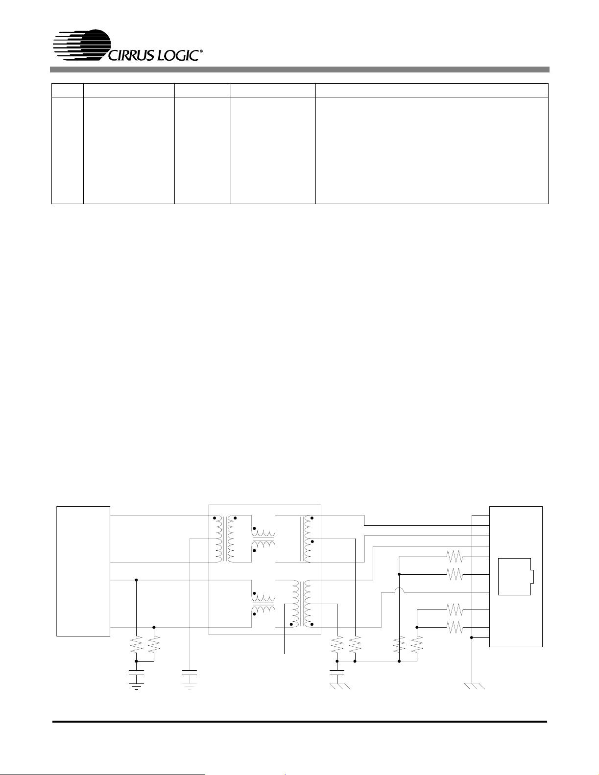
CS8952
BIT NAME TYPE RESET DESCRIPTION
0 Jabber Enable Read/Write 1 When set, the jabber function is enabled. When
clear, and if the CS8952 is in 10BASE-T full-duplex
or 10BASE-T ENDEC loopback mode, the jabber
function is disabled.
Note: When the National Compatibility Mode bit (bit
7) is set, the Jabber function may also be disabled
for 10BASE-T half-duplex, although this is not recommended.
7. DESIGN CONSIDERATIONS
The CS8952 is a mixed-signal device containing
the high-speed digital and analog circuits required
to implement Fast Ethernet communication. It is
important the designer adhere to the following
guidelines and recommendations for proper and reliable operation of the CS8952. These guidelines
will also benefit the design with good EMC performance.
7.1 Twisted Pair Interface
The recommended connection of the twisted-pair
interface is shown if Figure 6. The unused cable
pairs are terminated to increase the common-mode
performance. Common-mode performance is also
improved by connecting the center taps of the RX
T1
TG22-3506
CS8952
TX+
TX-
RX+
80
81
91
16
14
15
2
and TX input circuits to the DC-isolated ground
plane. The 0.01 µF capacitor C1 must provide 2KV
(1,500 Vrms for 60 seconds) of isolation to meet
802.3 requirements. If a shielded RJ45 connector is
used (recommended), the shield should be connected to chassis ground.
7.2 100BASE-FX Interface
Figure 7 shows the recommended connection for a
100BASE-FX interface to a Hewlett-Packard
HFBR-5103 fiber transceiver. Termination circuitry may need to be revised for other fiber transceivers. The FX Drive bit in the Loopback, Bypass, and
Receiver Error Mask Register (address 18h) may
be used to tailor the PECL interface for 50 Ω or
150 Ωloads.
10
12
11
6
5
51
51
51
Ω
Ω
Ω
SHLD
1
2
3
4
5
RJ-45
6
7
51
51
Ω
Ω
8
SHLD
92
RX-
49.9
Ω
0.1 µF 0.1 µF
49.9
1
Ω
3
NC
7
75
Ω
0.01 µF
2KV
75
Ω
51
Ω
Figure 6. Recommended Connection o f Twisted-Pair Ports (Network Interface Card)
CrystalLAN™ 100BASE-X and 10BASE-T Transceiver 63
Page 64

+5
CS8952
CS8952
SIGNAL-
SIGNAL+
TX_NRZ-
TX_NRZ+
RX_NRZ-
RX_NRZ+
8
9
4
5
6
7
68
191
82
130
Ω
Ω
Ω
Ω
+5
82
130
82
130
Ω
Ω
0.1 µF
49.9
Ω
Ω
+5 1 µH
Ferrite Bead
+5
0.1 µF 0.1 µF
1µH
Ω
63.4
Ω
49.9
Ω
Ferrite Bead
0.1 µF 0.1 µF
HFBR-5103
FIBER TRANS.
4
SD
5
RxV
CC
6
TxV
CC
7
TD-
8
TD+
3
RD-
2
RD+
1
RxV
EE
9
TxV
EE
Figure 7. Recommended Connection of Fiber Port
TX_NRZ+/- termination components should be
placed as close to the fiber transceiver as possible,
while RX_NRZ+/- and SIGNAL+/- termination
components should be placed close to the CS8952.
The CS8952 100BASE-FX interface IO pins
(TX_NRZ+, TX_NRZ-, RX_NRZ+, RX_NRZ-,
SIGNAL+, and SIGNAL-) may be left unconnected if a fiber interface is not used.
7.3 Internal Voltage Reference
A 4.99 kΩ biasing resistor must be connected between the CS8952 RES pin and ground. This resis-
tor biases the internal analog circuits of the CS8952
and should be placed as close as possible to RES
pin. Connect the other end of this resistor directly
to the ground plane. Connect the adjacent CS8952
ground pins (pins 85 and 87) to the grounded end of
the resistor forming a “shield” around the RES connection.
7.4 Clocking Schemes
The CS8952 may be clocked using one of three
possible schemes: using a 25 MHz crystal and the
internal oscillator, using an external oscillator sup-
64 CrystalLAN™ 100BASE-X and 10BASE-T Transceiver
Page 65

CS8952
e
87
VSS
RES
VSS
Figure 8. Biasing Resistor Connection and Layout
86
85
4.99 k
Ω
Via to
Ground Plan
plied through the XTAL_I pin, or using an external
clock source supplied through the TX_CLK pin.
CS8952
with transformers meeting these requirements.
However, the designer should evaluate the magnetics for suitability in their specific design.
7.6 Power Supply and Decoupling
The CS8952 supports connection to either a 3.3 V
or 5.0 V MII. When connected to a +5.0 V MII, all
power pins should be provided +5.0 V +/- 5%, and
all signal inputs should be referenced to +5.0V.
When interfaced with a 3.3 V MII, VDD_MII power pins should be provided +3.3 V +/- 5%, VDD
power pins should be provided +5.0 V +/- 5%, and
all signal inputs should be referenced to +3.3 V.
When a 25 MHz crystal is used, it should be placed
within one inch of the XTAL_I and XTAL_O pins
of the CS8952. The crystal traces should be short,
have no vias, and run on the component side.
Table 7 lists examples of manufacturers of suitable
crystals. The designer should evaluate their crystal
selection for suitability in their specific design.
An external CMOS clock source may be connected
to the XTAL_I pin, with the XTAL_O pin left
open. The input capacitance of the XTAL_I pin is
larger than the other inputs (a maximum of 35pF),
since it includes the additional load capacitance of
the crystal oscillator. Care should be taken to assure any external clock source attached to XTAL_I
is capable of driving higher capacitive loads. The
clock signal should be 25 MHz ±0.01% with a duty
cycle between 45% and 55%.
When the XTAL_I pin load is a problem, or only a
TTL level clock source is available, the CS8952
can be clocked through the TX_CLK pin, providing the TX_CLK mode is set appropriately using
the TCM pin. The clock frequency will be dependent on the operating mode.
7.5 Recommended Magnetics
The CS8952 requires an isolation transformer with
a 1:1 turns ratio for both the transmit and receive
signals. Table 7 lists examples of manufacturers
Component Manufacturer Part Number
Raltron Electronics Corp.
10651 NW 19th St.
Crystal
Transformer
Fiber
Interface
Table 7. Support Component Manufactures
Miami, FL 33172
(305) 593-6033
www.raltron.com
Halo Electronics, Inc.
P.O. Box 5826
Redwood City, CA 94063
USA
(650) 568-5800
www.haloelectronics.com
Bel Fuse, Inc.
198 Van Vorst Street
Jersey City, NJ 07302
USA
(201) 432-0463
www.belfuse.com
Pulse Engineering
12220 World Trade Drive
San Diego, CA 92128
USA
(619) 674-8100
www.pulseeng.com
Hewlett Packard
Component Sales
Response Center
(408) 654-8675
www.hp.com/HP-COMP
AS-25.000-15-FEXT-SMD-TRCIR
TG22-3506ND
S5558-5999-46
PE-68515
HFBR-5103
Each CS8952 power pin should be connected to a
0.1 µF bypass capacitor and then to the power
plane. The bypass capacitors should be located as
close to its corresponding power pin as possible.
Connect ground pins directly to the ground plane.
CrystalLAN™ 100BASE-X and 10BASE-T Transceiver 65
Page 66

CS8952
7.7 General Layout Recommendations
The following PCB layout recommendations will
help ensure reliable operation of the CS8952 and
good EMC performance.
• Use a multilayer Printed Circuit Board with at
least one ground and one power plane. A typical +5V MII application would be as follows:
Layer 1: (top) Components and first choice sig-
nal routing
Layer 2: Ground
Layer 3: Power (+5V)
Layer 4: (bottom) Second choice signal rout-
ing, bypass components
Place transformer TI as close to the RJ45 connec-
•
tor as possible with the secondary (network) side
facing the RJ45 and the primary (chip) side facing
the analog side (pins 76-100) of CS8952. Place
theCS8952inturnasclosetoT1aspos
• Use the bottom layer for signal routing as a second choice. You may place all components on
the top layer. However, bypass capacitors are
optimally placed as close to the chip as possible
and may be best located underneath the
CS8952 on the bottom layer. Termination components at the RJ-45 and fiber transceiver may
also be optimally placed on the bottom layer.
• Connect a 0.1 µF bypass capacitor to each
CS8952 VDD and VDD_MII pin. Place it as
close to its corresponding power pin as possible
and connect the other lead directly to the
ground plane.
• The 4.99K reference resistor should be placed
as close to the RES pin as possible. Connect the
other end of this resistor to the ground plane using a via. Connect the adjacent VSS pins (pins
85 and 87) to the grounded end of the resistor
forming a shield as illustrated in Figure 8.
• Controlled impedance is necessary for critical
signals TX+/-, RX+/-, TX_NRZ+/-, and
RX_NRZ+/-. These should be run as microstrip
sible.
transmission lines (100 Ωdifferential,50 Ωsingle-ended). The MII signals should be 68 Ωmicrostrip transmission lines. (For short MII
signal paths one may standardize on a given
trace width for all traces without significant
degradation in signal integrity.)
• Avoid routing traces other than the TX and RX
signals under transformer T1 and the RJ45 connector. Signals may run on the bottom side underneath the CS8952 as long as they stay away
from critical analog traces.
• Connect all CS8952 ground and power pins directly to the ground and power planes, respectively. Note: The VDD_MII power pins may
need their own power plane or plane segment in
+3.3 V MII applications.
• Depending on the orientation and location of
the transformer, the CS8952, and the RJ-45,
and on whether the application is for a NIC or a
switch,theRXandTXpairsmayneedtocross.
This should be done by changing layers on a
pair by pair basis only, using the minimum
number of vias, and making sure that each trace
within a pair “sees” the same path as its peer.
Figure 6 shows the CS8952 in a NIC or adapter
configuration. It may be configured for a hub or
repeater application by changing the wiring to
the RJ-45 as shown in Table 8.
• Differential pair transmission lines should be
routed close together (one trace width spacing
edge-to-edge) and kept at least two trace widths
away from other traces, components, etc. TX
and RX pairs should be routed away from each
other and may use opposite sides of the PCB as
necessary, Each member of the differential pair
should “see” the same PCB terrain as its peer.
• Unused spaces on the signal layers should be
filled with ground fill (pour). Vias should connect the ground patches to the ground plane.
This is especially recommended (symmetrical-
66 CrystalLAN™ 100BASE-X and 10BASE-T Transceiver
Page 67

ly) on both sides of the TX+/- traces.
CS8952
CS8952 Pin
Assignment
91 (RX+) 1 (RX+) 7 (RX+) 3 (RD+) 1 (RD+)
92 (RX-) 2 (RX-) 6 (RX-) 6 (RD-) 2 (RD-)
81 (TX-) 16 (TX-) 10 (TX-) 2 (TD+) 6 (TD-)
80 (TX+) 15 (TX+) 11(TX+) 1 (TD+) 3 (TD+)
T1 Primary Pin
Assignment
T1 Secondary
Pin Assignment
Table 8. RJ-45 Wiring
• No signal current carrying planes, i.e. no
ground or power plane, should be present underneath the region between the transformer
secondary (network) side and the RJ-45. However,achassisplanemaybeaddedinthisregion to pick up the metal tabs of a shielded RJ-
45. This chassis plane should be separated from
the ground and power planes by at least
50 mils. That is, all other ground and power
planes should be “cookie cuttered” so they are
voided in the area of the chassis plane. Generally speaking, parts should not cross the moat
except for the transformer.
• Proper termination practices must be used with
all transmission lines, especially if sending and
receiving high speed signals on and off the
board. Series terminations must be kept close to
the source and load terminations close to the
load. Thus the TX_NRZ+/- termination components must be kept close to the fiber optic
RJ-45 Pin Assignment
Adapter/NIC
Configuration
Hub/Repeater
Configuration
transceiver, and the RX_NRZ+/- and SIGNAL+/- termination components must be kept
close to the CS8952.
• Locate the crystal as close to the CS8952 as
possible, running short traces on the component
side in order to reduce parasitic load capacitance.
• Add bulk capacitance at each connector where
power may be supplied. For example, MII power may be provided at the MII connector and at
a separate connector for test purposes. If so, and
the two connectors are not adjacent, then the
bulk capacitors should be duplicated in each locations.
• Use wide traces to connect the “Bob Smith” termination resistors at T1 and the RJ-45 to the
2 KV capacitor or c apacitors in order to minimize their lead inductance.
CrystalLAN™ 100BASE-X and 10BASE-T Transceiver 67
Page 68

8. PIN DESCRIPTIONS
Pin Diagram
CS8952
VSS
VDD
VSS
TX_NRZ-
TX_NRZ+
RX_NRZ-
RX_NRZ+
SIGNAL-
SIGNAL+
VSS
VDD
VSS
VSS
RX_EN
RESET
REPEATER
CLK25
VSS
VDD
VSS
VDD_MII
VSS
10BT_SER
TEST0
TEST1
VDD
RSVD
RSVD
999897
100
1
2
3
4
5
6
7
8
9
10
11
12
13
14
15
16
17
18
19
20
21
22
23
24
25
26272829303132
VSS
XTAL_O
XTAL_I
VSS
VDD
96
949392919089888786
95
RX+
VSS
VDD
VDD
VSS
RX-
RES
CS8952 100-pin
TQFP
(14 mm x 14 mm)
33
35363738394041
34
VSS
VSS
85
RSVD
84
42
TX-
VDD
83828180797877
43
4546474849
44
TX+
VDD
VSS
RSVD
RSVD
76
RSVD
75
74
RSVD
73
LED5
LED4
72
LED3
71
LED2
70
LED1
69
SPD10
68
SPD100
67
VDD_MII
66
VSS
65
PWRDN
64
ISODEF
63
BPSCR
62
TXSLEW1
61
TXSLEW0
60
TCM
59
AN1
58
AN0
57
BP4B5B
56
VSS
55
VDD
54
VSS
53
BPALIGN
52
LPBK
51
50
VDD_MII
RX_DV/MII_DRV
VSS
RX_CLK
MDC
MDIO
MII_IRQ
68 CrystalLAN™ 100BASE-X and 10BASE-T Transceiver
RXD2
RXD0
RXD3/PHYA D3
RXD1/PHYAD1
VSS
VSS
VDD
TX_ER/TXD4
RX_ER/RXD4/P HYAD4
TX_CLK
TXD0
TX_EN
TXD3
TXD2
TXD1
LPSTRT
COL/PHYAD0
CRS/PHYAD2
Page 69

MII Interface Pins
COL/PHYAD0 - Collision Detect/PHY Address 0. Input/Tri-State Output, Pin 48.
Asserted active-high to indicate a collision on the medium during half-duplex operation. In full-duplex
operation, COL is undefined and should be ignored. When configured for 10 Mb/s operation, COL is
also used to indicate a Signal Quality Error (SQE) condition.
At power-up or at reset, the logic value on this pin is latched into bit 0 of the PHY Address field of the
Self Status Register (address 19h). This pin includes a weak internal pull-up (> 150 KΩ), or the value
may be set by an external 4.7 KΩ pull-up or pull-down resistor.
CRS/PHYAD2 - Carrier Sense/PHY Address 2. Input/Tri-State Output, Pin 49.
The operation of CRS is controlled by the REPEATER pin as follows:
REPEATER pin DUPLEX mode CRS Indicates
high don’t care receive activity only
low full duplex receive activity only
low half duplex receive or transmit activity
At power-up or at reset, the logic value of this pin is latched into bit 2 of the PHY Address Field of the
Self Status Register (address 19h). This pin includes a weak internal pull-down (> 20 KΩ), or the value
may be set by an external 4.7 KΩ pull-up or pull-down resistor.
CS8952
MDC - Management Data Clock. Input, Pin 28.
Input clock used to transfer serial data on MDIO. The maximum clock rate is 16.67 MHz. This clock may
be asynchronous to RX_CLK and TX_CLK.
MDIO - Management Data Input/Output. Bi-Directional, Pin 27.
Bi-directional signal used to transfer management data between the CS8952 and the Ethernet controller.
In order to conform with Annex 22B of the IEEE 802.3u specification, the MII_DRV pin should be pulled
high during power-up or reset, and the MDIO pin should have an external 1.5 KΩ pull-up resistor. For
systems not requir ed to drive external conne ctors and cables as descr ibed in the IEEE802.3u
specification, the external pull-up resistor may not be necessary.
MII_IRQ - MII Interrupt. Open Drain Output, Pin 26.
Asserted low to indicate the status corresponding to one of the unmasked interrupt status bits in the
Interrupt Status Register (address 11h) has changed. It will remain low until the ISR is read, clearing all
status bits.
This open drain pin requires a 4.7 kΩ pull-up resistor.
RX_CLK - Receive Clock. Tri-State Output, Pin 36
Continuous clock output used as a reference cloc k for sam pli ng RXD[3:0 ], RX_ ER, and RX _DV.
RX_CLK will have the following nominal frequency:
Speed 10BT_SER pin Nominal frequency
100 Mb/s n/a 25 MHz
10 Mb/s low (parallel) 2.5 MHz
10 Mb/s high (serial) 10 MHz
CrystalLAN™ 100BASE-X and 10BASE-T Transceiver 69
Page 70

CS8952
In order to conform with Annex 22B of the IEEE 802.3u specification, the MII_DRV pin should be pulled
high during power-up or reset, and the RX_CLK pin should have an external 33 Ω series resistor. For
systems not requir ed to drive external conne ctors and cables as descr ibed in the IEEE802.3u
specification, the external series resistor may not be necessary.
RX_DV/MII_DRV - Receive Data Valid/MII Drive Strength. Input/Tri-State Output, Pin 33.
Asserted high to indicate valid data nibbles are present on RXD[3:0].
At power-up or at reset, this pin is used as an input to determine the drive strength of the MII output
drivers. When the pin is low, all MII output drivers will be standard 4 mA CMOS drivers. When high,
additional drive strength will be added to the MII output drivers. This pin includes a weak internal pulldown (> 20 KΩ), or the value may be set by an external 4.7 KΩ pull-up or pull-down resistor.
In order to conform with Annex 22B of the IEEE 802.3u specification, this pin should be pulled high
during power-up or reset and should have an external 33 Ω series resistor. For systems not required to
drive external connectors and cables as described in the IEEE802.3u specification, it may be possible to
reduce overall power consumption by pulling the pin low at power-up or reset, and the external series
resistor may not be necessary.
RX_EN - Receive Enable. Input, Pin 14.
When high, signals RXD[3:0], RX_CLK, RX_DV, and RX_ER are enabled. When low, these signals are
tri-stated. RX_EN allows the received data signals of multiple PHY transceivers to share the same MII
bus.
This pin includes a weak internal pull-up (> 150 KΩ), or the value may be set by an external 10 KΩ pull-
up or pull-down resistor.
70 CrystalLAN™ 100BASE-X and 10BASE-T Transceiver
Page 71

CS8952
RX_ER/PHYAD4/RXD4 - Receive Error/PHY Address 4/Receive Data 4. Input/Tri-State Output,
Pin 37.
During normal MII operation, this pin is defined as RX_ER (Receive Error). When RX_DV is high,
RX_ER asserted high indicates that an error has been detected in the current receive frame. When
RX_DV is low and RXD[3:0] = “1110”, RX_ER high indicates a False Carrier condition.
If either BPALIGN or BP4B5B is asserted, then this pin is re-defined as RXD4 (Receive Data 4), the
most-significant bit of the received five-bit code-group. If the 4B5B encoder is being bypassed, receive
data is present when RX_DV is asserted. If alignment is being bypassed, data reception is continuous.
At power-up or at reset, the logic value on this pin is latched into bit 4 of the PHY Address field of the
Self Status Register (address 19h). This pin includes a weak internal pull-down (> 20 KΩ), or the value
may be set by an external 4.7 KΩ pull-up or pull-down resistor.
In order to conform with Annex 22B of the IEEE 802.3u specification, the MII_DRV pin should be pulled
high during power-up or reset, and the RX_ER pin should have an external 33 Ω series resistor. For
systems not requir ed to drive external conne ctors and cables as descr ibed in the IEEE802.3u
specification, the external series resistor may not be necessary.
RXD3/PHYAD3 - Receive Data 3/PHY Address 3. Tri-State Output, Pin 29.
RXD2 - Receive Data 2. Tri-State Output, Pin 30.
RXD1/PHYAD1 - Receive Data 1/PHY Address 1. Tri-State Output, Pin 31.
RXD0 - Receive Data 0. Tri-State Output, Pin 32.
Receive data output. Receive data is present when RX_DV is asserted. RXD0 is the least-significant bit.
For MII modes, nibble-wide data (synchronous to RX_CLK) is transferred on pins RXD[3:0]. In 10 Mb/s
serial mode, pin RXD0 is used as the serial output pin, and RXD[3:1] are ignored. When either BP4B5B
or BPALIGN is selected, pin RXD4 contains the most-significant bit of the five-bit code-group.
At power-up or at reset, the value on RXD1/PHY AD1 is latched into bit 1 of the PHY Address field of
the Self Status Register (address 19h). This pin includes a weak internal pull-down (> 20 KΩ), or the
value may be set by an external 4.7 KΩ pull-up or pull-down resistor.
At power-up or at reset, the logic value on RXD3/PHYAD3 is latched into bit 3 of the PHY Address field
of the Self Status Register (address 19h). This pin includes a weak internal pull-down (> 20 KΩ), or the
value may be set by an external 4.7 KΩ pull-up or pull-down resistor.
In order to conform with Annex 22B of the IEEE 802.3u specification, the MII_DRV pin should be pulled
high during power-up or reset, and the RXD[3:0] pins should have external 33 Ω series resistors. For
systems not requir ed to drive external conne ctors and cables as descr ibed in the IEEE802.3u
specification, the external series resistors may not be necessary.
TX_CLK - Transmit Clock. Input/Tri-State Output, Pin 42.
Continuous clock signal used by the CS8952 as a reference clock to sample TXD[3:0], TX_ER, and
TX_EN. TX_CLK can be referenced either internally (Output Mode) or externally (Input Mode) based
upon the value of the TCM pin at power-up or at reset.
TCM pin TX_CLK mode CLK25 status
high TX_CLK is input CLK25 pin is an output
floating TX_CLK is input CLK25 is disabled
low TX_CLK is output CLK25 is disabled
CrystalLAN™ 100BASE-X and 10BASE-T Transceiver 71
Page 72

WhentheTCMpinishighonpower-uporreset,theCLK25pinmaybeusedasasourceforthe
TX_CLK pin. When the TCM pin is floating on power-up or reset, TX_CLK must be supplied externally.
TX_CLK should have the following nominal frequency:
Speed 10BT_SER pin Nominal frequency
100 Mb/s n/a 25 MHz
10 Mb/s low (parallel) 2.5 MHz
10 Mb/s high (serial) 10 MHz
TX_EN - Transmit Enable. Input, Pin 43.
Asserted high to indicate valid data nibbles are present on TXD[3:0]. When BPALIGN is selected,
TX_ENmustbepulleduptoVDD_MII.
TX_ER/TXD4 - Transmit Error Encoding/Transmit Data 4. Input, Pin 38.
When high, TX_ER indicates to the CS8952 that a transmit error has occurred. If TX_ER is asserted
simultaneously with TX_EN in 100 Mb/s mode, the CS8952 will ignore the data on the TXD[3:0] pins
and transmit one or more 100 Mb/s HALT symbols in its place. In 10 Mb/s mode, TX_ER has no effect
on the transmitted data.
If BP4B5B or BPALIGN are set, TX_ER/TXD4 is used to transmit the most-significant bit of the five-bit
code group.
CS8952
TXD[3:0] - Transmit Data. Input, Pins 47, 46, 45, and 44.
Transmit data input pins. For MII modes, nibble-wide data (synchronous to TX_CLK) must be presented
on pins TXD[3:0] when TX_EN is asserted high. TXD0 is the least significant bit. In 10 Mb/s serial
mode, pin TXD0 is used as the serial input pin, and TXD[3:1] are ignored.
When either BP4B5B or BPALIGN is selected, pin TXD4 contains the most significant bit of the five-bit
code-group.
Control and Status Pins
10BT_SER - 10 Mb/s Serial Mode Select. Input, Pin 23.
When asserted high during power-up or reset and 10 Mb/s operation is selected, serial data will be
transferred on pins RXD0 and TXD0. When low during power-up or reset and 10 Mb/s operation is
selected, data is transferred a nibble at a time on RXD[3:0] and TXD[3:0]. This pin is ignored during
100 Mb/s operation.
10 Mb/s serial mode may also be entered under software control through bit 9 of the 10BASE-T Status
Register (address 1Bh).
At power-up or at reset, the value on this pin is latched into bit 9 of the 10BASE-T Status Register
(address 1Bh). This pin includes a weak internal pull-down (> 20 KΩ), or the value may be set by an
external 4.7 KΩ pull-up or pull-down resistor.
AN[1:0] - Auto-Negotiate Control. Input, Pins 58 and 57.
These three-level input pins are sampled during power-up or reset. They control the forced or
advertised auto-negotiation operating modes. If one of these pins is left unconnected, internal logic pulls
its signal to a mid-range value, 'M'.
AN1 pin AN0 pin Speed Forced/Auto Full/Half Duplex
0 M 10 Mb/s Forced Half
72 CrystalLAN™ 100BASE-X and 10BASE-T Transceiver
Page 73

CS8952
AN1 pin AN0 pin Speed Forced/Auto Full/Half Duplex
1 M 10 Mb/s Forced Full
M 0 100 Mb/s Forced Half
M 1 100 Mb/s Forced Full
M M 100/10 Mb/s Auto-Neg Full/Half
0 0 10 Mb/s Auto-Neg Half
0 1 10 Mb/s Auto-Neg Full
1 0 100 Mb/s Auto-Neg Half
1 1 100 Mb/s Auto-Neg Full
Auto-Negotiation may also be enabled and the advertised capabilities modified under software control
through bit 8 of the Basic Mode Control Register (address 00h), and bits 5, 6, 7, 8, and 10 of the AutoNegotiation Advertisement Register (address 04h).
These pins are pulled to ‘M’ through weak internal resistors (> 150 KΩ). Other values may be set by
tying them directly to VDD_MII or VSS, or through external 10 KΩ pull-up or pull-down resistors.
CrystalLAN™ 100BASE-X and 10BASE-T Transceiver 73
Page 74

BP4B5B - Bypass 4B5B Coders. Input, Pin 56.
When driven high during power-up or reset, the transmit 4B5B encoder and receiver 5B4B decoder are
bypassed. Five-bit code groups are output and input on pins RXD[4:0] and TXD[4:0].
The 4B5B Coders may also be bypassed under software control through bit 14 of the Loopback,
Bypass, and Receiver Error Mask Register (address 18h).
At power-up or at reset, the value on this pin is latched into bit 14 of the Loopback, Bypass and
Receiver Error Mask Register (address 18h). This pin includes a weak internal pull-down (> 20 KΩ), or
the value may be set by an external 4.7 KΩ pull-up or pull-down resistor.
BPALIGN - Bypass Symbol Alignment. Input, Pin 52.
When driven high during power-up or reset, the following blocks are bypassed: 4B5B encoder, 5B4B
decoder, scrambler, descrambler, NRZI encoder, and NRZI decoder. Five-bit code groups are output and
input on pins RXD[4:0] and TXD[4:0]. The receiver will output five-bit data with no attempt to identify
code-group boundaries; therefore, the data in one RXD[4:0] word may contain data from two code
groups.
Symbol alignment may also be bypassed under software control through bit 12 of the Loopback,
Bypass, and Receiver Error Mask Register (address 18h).
At power-up or at reset, the value on this pin is latched into bit 12 of the Loopback, Bypass and
Receiver Error Mask Register (address 18h). This pin includes a weak internal pull-down (> 20 KΩ), or
the value may be set by an external 4.7 KΩ pull-up or pull-down resistor.
CS8952
BPSCR - Bypass Scrambler. Input, Pin 62.
When driven high during power-up or reset, the scrambler and descrambler is bypassed and NRZI FX
mode is selected.
The 100BASE-FX mode may also be entered under software control through bit 13 of the Loopback,
Bypass, and Receiver Error Mask Register (address 18h).
At power-up or at reset, the value on this pin is latched into bit 13 of the Loopback, Bypass and
Receiver Error Mask Register (address 18h). This pin includes a weak internal pull-down (> 20 KΩ), or
the value may be set by an external 4.7 KΩ pull-up or pull-down resistor.
74 CrystalLAN™ 100BASE-X and 10BASE-T Transceiver
Page 75

ISODEF - Isolate Default. Input, Pin 63.
When asserted high during power-up or reset, the MII will power-up electrically isolated except for the
MDIO and MDC pins. When low, the part will exit reset fully electrically connected to the MII.
The MII may also be isolated under software control through bit 10 of the Basic Mode Control Register
(address 00h).
At power-up or at reset, the value on this pin is latched into bit 10 of the Basic Mode Control Register
(address 00h). This pin includes a weak internal pull-down (> 20 KΩ), or the value may be set by an
external 4.7 KΩ pull-up or pull-down resistor.
LED1 - Transmit Active LED. Open Drain Output, Pin 69.
This active-low output indicates transmit activity. It contains a pulse stretcher to insure that the transmit
eventsarevisiblewhenthepinisusedtodriveanLED.Thedefinitionofthispinmaybemodifiedto
indicate Disconnect Detection (bit 5 of the Self Status Register (address 19h)) by setting bit 2 of the
PCS Sub-layer Configuration Register (address 17h).
This pin can be simultaneously connected to an LED and to a TTL-compatible, CMOS input pin.
LED2 - Receive Activity LED. Open Drain Output, Pin 70.
This active-low output indicates receive activity. It contains a pulse stretcher to insure that the receive
events are visible when the pin is used to drive an LED.
CS8952
This pin can be simultaneously connected to an LED and to a TTL-compatible, CMOS input pin.
LED3 - Link Good LED. Open Drain Output, Pin 71.
This active-low output indicates the CS8952 has detected a valid link.
This pin can be simultaneously connected to an LED and to a TTL-compatible, CMOS input pin.
LED4 - Polarity/Full Duplex LED. Open Drain Output, Pin 72.
This active-low output indicates:
1) for 100 Mb/s operation, the CS8952 is in full-duplex operation,
2) for 10 Mb/s operation, either good polarity exists or full duplex is selected (see bit 1 in the PCS Sublayer Configuration Register (address 17h)).
This pin can be simultaneously connected to an LED and to a TTL-compatible, CMOS input pin.
LED5 - Collision/Descrambler Lock LED. Open Drain Output, Pin 73.
This active-low output is asserted when either the CS8952 detects a collision (bit 11 of the PCS SubLayer Configuration Register (address 17h) is clear), or the 100BASE-TX descrambler is synchronized
(bit 11 of the PCS Sub-Layer Configuration Register (address 17h) is set). It contains a pulse stretcher
to insure that the collision events are visible when the pin is used to drive an LED.
This pin can be simultaneously connected to an LED and to a TTL-compatible, CMOS input pin.
LPBK - Loopback Enable. Input, Pin 51.
When this pin is asserted high and the CS8952 is operating in 100 Mb/s mode, the CS8952 will perform
a local loopback inside the PMD block, routing the scrambled NRZI output to the NRZI input port on the
descrambler. The loopback includes all CS8952 100 Mb/s functionality except the MLT-3 coders and the
analog line interface blocks.
When asserted high and the CS8952 is operating in 10 Mb/s mode, the CS8952 will perform a local
ENDEC loopback.
CrystalLAN™ 100BASE-X and 10BASE-T Transceiver 75
Page 76

LPSTRT - Low Power Start. Input, Pin 50.
When this active-low input is asserted during power-up or reset, the CS8952 will exit reset in a low
power configur ation , w here the only ci rcui try enabled is t hat necessary to maintain the media
impedance. The CS8952 will remain in a low power state until RESET pin is asserted or the MDC pin
toggles.
This pin includes a weak internal pull-down (> 20 KΩ), or the value may be set by an external 4.7 KΩ
pull-up or pull-down resistor.
PWRDN - Power Down. Input, Pin 64.
When this pin is asserted high, the CS8952 powers down all circuitry except that circuitry needed to
maintain the network line impedance. This is the lowest power mode possible. The CS8952 will remain
in low power mode until the PWRDN pin is deasserted.
A slightly higher power power-down mode may also be entered under software control through bit 11 of
the Basic Mode Control Register (address 00h).
CS8952
76 CrystalLAN™ 100BASE-X and 10BASE-T Transceiver
Page 77

REPEA TER - REPEATER Mode Select. Input, Pin 16.
This pin controls the operation of the CRS (Carrier Sense) pin as shown below:
REPEATER pin DUPLEX mode CRS Indicates
high don’t care receive activity only
low full duplex receive activity only
low half duplex receive or transmit activity
At power-up or at reset, the value on this pin is latched into bit 12 of the PCS Sub-Layer Configuration
Register (address 17h). This pin includes a weak internal pull-down (> 20 KΩ), or the value may be set
by an external 4.7 KΩ pull-up or pull-down resistor.
SPD10 - 10 Mb/s Speed Indication. Output, Pin 68.
This pin is asserted high when the CS8952 is configured for 10 Mb/s operation. This pin can be used to
drive a low-current LED to indicate 10 Mb/s operation.
SPD100 - 100 Mb/s Speed Indication. Output, Pin 67.
This pin is asserted high when the CS8952 is configured for 100 Mb/s operation. This pin can be used
to drive a low-current LED to indicate 100 Mb/s operation.
TCM - Transmit Clock Mode Initialization. Input, Pin 59.
The logic value on this three-level pin during power-up or reset determines whether TX_CLK is used as
an input or an output, and whether an external 25 MHz clock reference is provided on the CLK25 output
pin.
CS8952
TCM pin TX_CLK mode CLK25 status
high TX_CLK is input CLK25 pin is an output
floating TX_CLK is input CLK25 is disabled
low TX_CLK is output CLK25 is disabled
TEST[1:0] - Factory Test. Input, Pins 24 and 25.
These pins are for factory test only. They include weak internal pull-downs (> 20 KΩ), and should be tied
directly to VSS for normal operation.
CrystalLAN™ 100BASE-X and 10BASE-T Transceiver 77
Page 78

TXSLEW[1:0] - Transmit Slew Rate Control. Input, Pins 61 and 60.
These three-level pins allow adjustment to the rise and fall times of the 10BASE-TX transmitter output
waveform. The rise and fall times are symmetric.
TXSLEW0 pin TXSLEW1 mode Rise/Fall time
low low 0.5 ns
low floating 1.0 ns
low high 1.5 ns
floating low 2.0 ns
floating floating 2.5 ns
floating high 3.0 ns
high low 3.5 ns
high floating 4.0 ns
high high 4.5 ns
Media Interface Pins
RX+, RX- - 10/100 Receive. Differential Input Pair, Pins 91 and 92.
Differential input pair receives 10 or 100 Mb/s data from the receive port of the transformer primary.
CS8952
TX+, TX- - 10/100 Transmit. Differential Output Pair, Pins 80 and 81.
Differential output pair drives 10 or 100 Mb/s data to the transmit port of the transformer primary.
RX_NRZ+, RX_NRZ- - FX Receive. Differential Input Pair, Pins 6 and 7.
PECL output pair receives 100 Mb/s NRZI-encoded data from an external optical module.
SIGNAL+, SIGNAL- - Signal Detect. Differential Input Pair, Pins 9 and 8.
PECL input pair receives signal detection indication from an external optical module.
TX_NRZ+, TX_NRZ- - FX Transmit. Differential Output Pair, Pins 5 and 4.
PECL output pair drives 100 Mb/s NRZI-encoded data to an external optical module.
General Pins
CLK25-25MHzClock.Output,Pin17.
A 25 MHz Clock is output on this pin when the CS8952 is configured to use an external reference
transmit clock in TX_CLK IN MASTER mode. See the pin description for the Transmit Clock Mode
Initialization pin (TCM) for more information on TX_CLK operating modes.
CLK25 may also be enabled regardless of the TCM pin state by clearing bit 7 of the PCS Sub-layer
Configuration Register (address 17h).
RES - Reference Resistor. Input, Pin 86.
This input should be connected to ground with a 4.99 kΩ +/-1% series resistor. The resistor is needed
for the biasing of internal analog circuits.
78 CrystalLAN™ 100BASE-X and 10BASE-T Transceiver
Page 79

RESET - Reset. Input, Pin 15.
This active high input initializes the CS8952, and causes the CS8952 to latch the input signal on the
following pins: COL/PHYAD0, CRS/PHYAD2, RX_ER/PHYAD4/RXD4, 10BT_SER, BP4B5B, BPALIGN,
BPSCR, ISODEF, REPEATER, RXD[1]/PHYAD1, and RXD[3]/PHYAD3.
XTAL_I - Crystal Input, Pin 96.
XTAL_O - Crystal Output, Pin 97.
A 25 MHz crystal should be connected across pins XTAL_I and XTAL_O. If a crystal is not used, a
25 MHz CMOS level clock may be connected to XTAL_I and XTAL_O left open.
NOTE: The XT AL_I pin capacitive load may be as high as 35pF . Any external clock source connected to this
pin must be capable of driving larger capacitive loads.
RSVD - Reserved. Pins 74, 75, 76, 77, 84, 98, and 99.
These seven pins are reserved and should be tied to VSS.
VDD_MII - MII Power. Pins 21, 34, and 66.
These pins provide power to the CS8952 MII interface. Typically VDD_MII will be either +5V or +3.3V.
VDD - Core Power. Pins 2, 11, 19, 40, 54, 79, 82, 88, 89, 94, and 100.
These pins provide power to the CS8952 core. Typically, VDD should be +5V.
CS8952
VSS - Ground. Pins 1, 3, 10, 12, 13, 18, 20, 22, 35, 39, 41, 53, 55, 65, 78, 83, 85, 87, 90, 93, and 95.
These pins provide a ground reference for the CS8952.
CrystalLAN™ 100BASE-X and 10BASE-T Transceiver 79
Page 80

9. PACKAGE DIMENSIONS
100L TQFP PACKAGE DRAWING
D1
D
CS8952
E
E1
1
e
B
∝
L
INCHES MILLIMETERS
DIM MIN MAX MIN MAX
A --- 0.063 --- 1.60
A1 0.002 0.006 0.05 0.15
B 0.007 0.011 0.17 0.27
D 0.618 0.642 15.70 16.30
D1 0.547 0.555 13.90 14.10
E 0.618 0.642 15.70 16.30
E1 0.547 0.555 13.90 14.10
e* 0.016 0.024 0.40 0.60
L 0.018 0.030 0.45 0.75
∝
* Nominal pin pitch is 0.50 mm
Controlling dimension is mm.
JEDEC Designation:MS026
0.000° 7.000° 0.00° 7.00°
A
A1
80 CrystalLAN™ 100BASE-X and 10BASE-T Transceiver
Page 81

• Notes •
Page 82

 Loading...