

Page 1

1
Features
■ Buffered Speed Sensor
Output
■ No Cross-conduction in
either H-bridge
■ Guaranteed Monotonic
■
On Chip Flyback Diodes
■ Fault Protection
Overvoltage
Short Circuit Protection
Load Dump Protection
to 60V
Package Options
8L PDIP
CS8442
85mA Dual H-Bridge Odometer Driver
with Buffered Speed Signal Output
Description
Block Diagram
Absolute Maximum Ratings
The CS8442 is a stepper motor
driver that implements an Hbridge design to drive two coils in
an eight step sequence each revolution. Each H-bridge is capable of
delivering 85mA to the load.
The sequencer function insures
that the odometer is monotonic
and that cross-conduction of each
H bridges does not occur. Before
the beginning of each sequence,
both bridges are turned off. This
Òdead zoneÓ minimizes the fly
back energy generated in the
inductive loads. In addition, on
board clamp diodes across each
output protect the output drive
transistors from excessive fly back
voltages.
The CS8442 is fault protected
against reverse battery, short circuit, and over voltage conditions.
If a fault is detected, the IC shuts
down.
The buffered speed signal output
(SENSOR OUT) is an open collector NPN capable of driving a
4.7k½ load connected to a 5V supply. The signal is a buffered,
inverted version of the speed sensor input voltage (SENSOR IN).
The input voltage can be either a
sine or square wave form.
CS8442
Supply Voltage (VCC) (continuous) -40ûC to +105ûC ..................Ð0.5 to 24V
(100ms pulse transient) -40ûC to +105ûC ......................Ð0.5 to 60V
Input Voltage (VIN) ..............................................................Ð0.3 to VCC+0.3V
Storage Temperature Range (T
STG
)......................................Ð65¡C to +150¡C
Junction Temperature.............................................................Ð40¡C to +150¡C
Speed Sensor Output .....................................................................................7V
ESD (Human Body Model) .........................................................................2kV
Lead Temperature Soldering
Wave Solder (through hole styles only)........10 sec. max, 260¡C peak
Cherry Semiconductor Corporation
2000 South County Trail, East Greenwich, RI 02818
Tel: (401)885-3600 Fax: (401)885-5786
Email: info@cherry-semi.com
Web Site: www.cherry-semi.com
A Company
¨
Rev. 8/2/93
SENSOR
IN
Input
Comp.
Coil
Driver
A
COILA+
COILA-
1
Gnd
COILA+
COILAÐ
SENSOR
IN
V
CC
COILB+
COILBÐ
SENSOR
OUT
SENSOR
OUT
Sequencer
Overvoltage
and Short
Circuit
Protection
Coil
Driver
B
COILB
+
COILB-
Page 2
2
CS8442
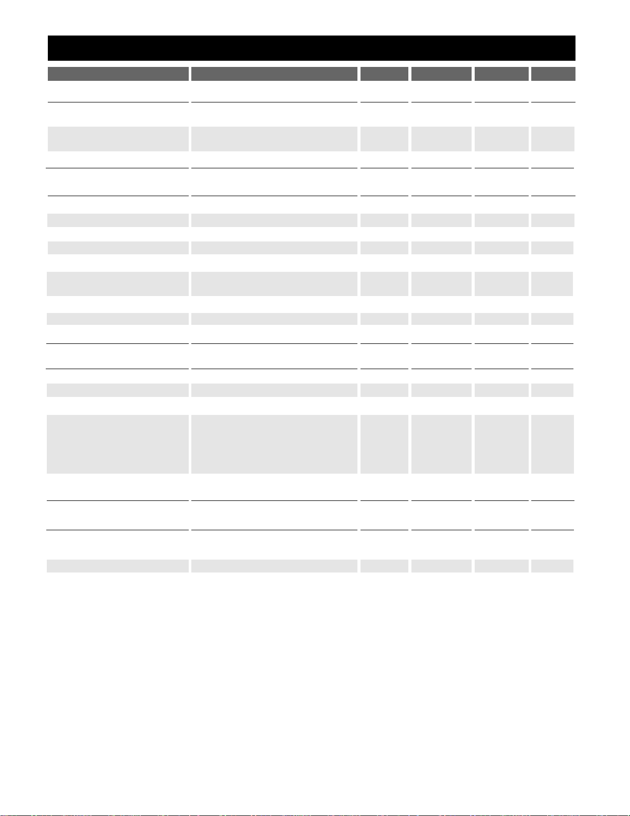
Electrical Characteristics: Unless otherwise stated, these specifications apply for -40ûC to +105ûC, V
CC
= 6.5 to 15.5 VDC. All
voltage shall be referenced to Gnd unless otherwise noted. Overvoltage shutdown of coils occurs when V
CC
>16V.
PARAMETER TEST CONDITIONS MIN TYP MAX UNIT
* Voltage across the coils shall be measured at the specific voltages, but shall also be within linearly interpolated limits.
■ Supply
Supply Voltage Range TA= -40¡C to +105¡C 6.5 15.5 a
TA= -40¡C to +25¡C 6.5 24.0 a
Supply Current VCC= 15.5 VDC 35 mA
Outputs not loaded
Overvoltage Shutdown 16 23 V
■ Speed Sensor
Input Frequency Range 0 400 Hz
Switching Threshold 1.6 3.0 VDC
Hysteresis 300 mV
Input Bias Current VIN= 0.8VDC to V
CC
±1 µA
Input Voltage Range 0 8 VDC
Operating Input Voltage 10K Ohm Resistor in Series -15 VDC
to V
CC
Output Saturation Voltage ICC=1.3mA 0.4 V
Output Leakage VCC=5.5V 10 µA
Input Clamp Current I Clamp at VIN= 0 VDC -0.4 -5.0 mA
■ Coil Output Drivers
Coil Load +25¡C 198 210 222 ½
Coil Inductance 80 mH
Coil Resistance Temperature Coefficient 0.39 %/¡C
* Energized Coil Voltage
(Both Polarities) A and B VCC= 6.5 VDC VCC-1.50 VDC
VCC= 10.0 VDC VCC-1.60 VDC
VCC= 15.5 VDC,TA= -20¡C to +105¡C VCC-1.75 VDC
VCC= 15.5 VDC,TA= -40¡C to -20¡C VCC-2.00 VDC
De-Energized Coil Leakage ±100 µA
Current
■ Short Circuit Protection
Short Circuit Threshold 275 400 mA
Coil A + Coil B
Short Circuit Turn Off Delay 5 µs
Page 3

3
SENSOR IN is a PNP comparator input that accepts a sine or
square wave input. Signals in excess of V
CC
or Ground will not
damage the input as long as the input current is limited to
1.5mA. An active clamp at 0V prevents negative input voltages
from disrupting normal operation. The input can withstand 150
VDC as long as the input current does not exceed 1.5mA. This is
possible if a 100k½ resistor is placed in series with the SENSOR
IN.
SENSOR OUT is an open collector NPN transistor that produces
a buffered and inverted version of the SENSOR IN signal. It is
capable of driving a 4.7k½ load connected to a 5V supply.
The eight step sequencer moves the two H bridge output drivers
through 8 sequential states (Table 1, Figure 1). In State 0, current
flows from COILA+ out through COIL A and back in through
COILA-. The same polarity also holds for COIL B. In State 1,
COIL A outputs turn off while COIL B outputs continue conducting with the same polarity. In State 2, current flows from
COIL A- out through the coil and back in COIL A+. COIL B outputs continue with their original polarity. COIL A outputs
maintain this polarity through States 3 and 4 during which
COIL B outputs are first turned off and then reversed. COIL BÕs
reversed polarity continues in Stages 5 and 6. COIL AÕs outputs
are turned off in Stage 5 and then turned back on (positive
polarity) in Stage 6. In Stage 7, COIL B is off and COILA outputs
continue with a positive polarity.
Table 1: Transition States
The polarity definition for the coil driver outputs is as follows:
Connect Connect
Polarity Coil + Coil -
Positive (+) V
CC
Gnd
Negative (-) Gnd V
CC
Each H-bridge output stage consists of 4 power NPN transistors
with fly back diodes (Figure 2). Each half bridge has a composite
saturation voltage of 1.5V at V
CC
=15.5V and I
OUT
= 85mA.
The output stage is designed to prevent cross conduction: i.e., at
no time can Q1 and Q2 or Q3 and Q4 conduct. This dead zone
time minimizes fly back energy and helps protect the output
stages from damage.
The CS8442 is protected from short circuit, over voltage and
thermal runaway conditions. When any of these faults is detected, an internal flip-flop is set and both H bridges are disabled.
When the fault condition is removed, the Flip-Flop is reset after
the first positive going edge from the speed sensor input.
CS8442
Package Pin Description
Application Information
Speed Sensor
Sequencer
H Bridge Outputs A and B
Protection Circuitry
PACKAGE PIN # PIN SYMBOL FUNCTION
8L PDIP
1 Gnd Ground connection.
2 COILA+ Output stage, when active, supplies current to COIL A.
3 COILA- Output stage, when active, supplies current to COIL A.
4 SENSOR IN Input signal from wheel speed or engine rpm.
5 SENSOR OUT Buffered and inverted output of SENSOR IN signal.
6 COILB- Output stage, when active, supplies current to COIL B.
7 COILB+ Output stage, when active, supplies current to COIL B.
8VCCSupply Voltage.
Figure 2: Coil Driver Output
Figure 1: State Diagram for Coil Outputs
Output State Table
State Coil A Coil B
0++
1 OFF +
2-+
3 - OFF
4-5 OFF 6+7 + OFF
0
STATE #
+
COIL A
Ð
+
COIL B
Ð
1 2 3 4 5 6 7 0
Q1
Q2
Short
Circuit
Sense
Resistor
Q3
Q4
Short
Circuit
Sense
Resistor
Coil
V
Gnd
CC
Overvoltage
and
Short
Circuit
Protection
Page 4

4
Part Number Description
CS8442XN8 8L PDIP
Thermal Data 8L PDIP
RQ
JC
typ 52 ûC/W
RQ
JA
typ 100 ûC/W
Package Specification
Application Diagram
PACKAGE DIMENSIONS IN mm (INCHES)
Ordering Information
PACKAGE THERMAL DATA
Rev. 8/2/93
D
Lead Count Metric English
Max Min Max Min
8L PDIP 10.16 9.02 .400 .355
CS8442
C1 - 10µF
C2 - 0.1µF
C3 - 0.01µF
R1 - 3.9½ 0.5W
R2 - 100k½
R3 - 15k½
D1 - 1A 600PIV
Z1 - 50V 0.5W
COIL A - 210±12½, 80mH
COIL B - 210±12½, 80mH
0.39 (.015)
MIN.
2.54 (.100) BSC
1.77 (.070)
1.14 (.045)
D
Some 8 and 16 lead
packages may have
1/2 lead at the end
of the package.
All specs are the same.
.203 (.008)
.356 (.014)
REF: JEDEC MS-001
3.68 (.145)
2.92 (.115)
8.26 (.325)
7.62 (.300)
7.11 (.280)
6.10 (.240)
.356 (.014)
.558 (.022)
Plastic DIP (N); 300 mil wide
© 1999 Cherry Semiconductor Corporation
Cherry Semiconductor Corporation reserves the
right to make changes to the specifications without
notice. Please contact Cherry Semiconductor
Corporation for the latest available information.
IGN
Buffered Speed Signal
(Open Collector Drive)
D1
R1
COILA+ COILAÐ COILB+ COILBÐ
CS8442
V
CC
R3
Z1
C1
R2
C2
C3
SENSOR IN
SENSOR OUT Gnd
 Loading...