

Datasheet CS8402A-IS, CS8402A-IP, CS8402A-CS, CS8402A-CP, CS8401A-IS Datasheet (Cirrus Logic)
...Page 1
CS8401A
CS8402A
Digital Audio Interface Transmitter
Features
l
Monolithic Digital Audio Interface Transmitter
l
Supports: AES/EBU, IEC958, S/PDIF, &
EIAJ CP-340 Professional and Consumer
Formats
l
Host Mode and Stand Alone Modes
l
Generates CRC Codes and Parity Bits
l
On-Chip RS422 Line Driver
l
Configurable Buffer Memory (CS8401A)
l
Transparent Mode Allows Direct Connection
of CS8402A and CS8412 or CS8401A and
CS8411A
I
CS8401A
6
SCK
FSYNC
SDATA
CS
RD/WR
A4-A0
D7-D0
7
8
14
16
5
8
Audio
Serial Port
Configurable
Buffer
Memory
Description
The CS8401/2A are monolithic CMOS devices which encode and transmit audio data according to the AES/EBU,
IEC958, S/PDIF, & EIAJ CP-340 interface standards.
The CS8401/2A accept audio and digital data, which is
then multiplexed, encoded and driven onto a cable. The
audio serial port is double buffered and capable of supporting a wide variety of formats.
The CS8401A has a configurable internal buffer memory, loaded via a parallel port, which may be used to buffer
channel status, auxiliary data, and/or user data.
The CS8402A multiplexes the channel, user, and validity
data directly from serial input pins with dedicated input
pins for the most important channel status bits.
ORDERING INFORMATION
See page 30.
INT
15
MUX
MCK
5
Prescaler
RS422
Driver
TXP
20
TXN
17
CS8402A
6
SCK
FSYNC
SDATA
Cirrus Logic, Inc.
Crystal Semiconductor Products Division
P.O. Box 17847, Austin, Texas 78760
(512) 445 7222 FAX: (512) 445 7581
http://www.crystal.com
7
8
10
C
11
U
9
V
M223M122M0
Audio
Serial Port
Registers
21
MUX
7
15
Dedicated Channel
Status Bits
Copyright Cirrus Logic, I nc. 1997
(All Rights Reserv ed)
CBL24TRNPT
MCK
RST
5
RS422
Driver
16
TXP
20
TXN
17
NOV ‘93
DS60F1
1
Page 2
CS8401A CS8402A
ABSOLUTE MAXIMUM RATINGS (GND = 0V, all voltages with respect to ground.)
Parameter Symbol Min Max Units
DC Power Supply VD+ 6.0 V
Input Current, Any Pin Except Supply Note 1 I
Digital Inpu t Voltage V
Ambient Operat ing Temper ature (po wer applie d) T
Storage Temperature T
Notes: 1. Transient currents of up to 100 mA will not cause SCR latch-up.
WARNING: Operation at or beyond these limits may result in permanent damage to the device.
Normal oper ation is not g uaran teed a t thes e extre mes.
in
IND
A
stg
-
-0.3 VD+ V
-55 125
-65 150
10 mA
±
RECOMMENDED OPERATING CONDITIONS
(GND = 0V; all voltages with respect to ground)
Parameter Symbol Min Typ Max Units
DC Voltage VD+ 4.5 5.0 5.5 V
Supply Current Note 2 I
Ambient Ope rating Temper ature: CS8401/2A-C P or - CS Note 3 T
CS8401/2A-IP or -IS -40 85
Power Consumption Note 2 P
Notes: 2. Drivers open (unlo aded). The ma jority of pow er is used in the load con nected to th e drivers.
3. The ’-CP’ and ’-CS’ pa rts are spec ified to ope rate over 0 to 70 °C but are tested at 25 °C only.
The ’-IP’ and ’-I S’ parts are te sted over the full -40 to 85 °C temperature range.
DD
A
D
02570
1.5 5 mA
7.5 25 mW
C
°
C
°
C
°
C
°
DIGITAL CHARACTERISTICS
(TA = 25 °C for suffixes ’CP’ & ’CS’, TA = -40 to 85 °C for ’IP’ & ’IS’; VD+ = 5V ± 10%)
Parameter Symbol Min Typ Max Units
High-Level Input Voltage V
Low-Level Input Voltage V
High-Level Output Voltage (IO = 200µA) V
Low-Level Ou tput V oltage (IO = 3.2mA) V
Input Leakage Current I
Master Clock Frequency: CS8401A Note 4 MCK 22 MHz
CS8402A Note 4 7.1 M Hz
Master Clock Duty Cycle CS8401/2A 40 60 %
Notes: 4. MCK for the CS8401 must be 128, 192, 256, or 384× the input word rate based on M0 and M1 in control
register 2. MCK for the CS8402A must be 128× the input word rate, except in Transparent Mode where MCK is
256x the input word rate.
IH
IL
OH
OL
in
Specifications are subject to change without notice.
2 DS60F1
2.0 VDD+0.3 V
-0.3 +0.8 V
VDD-1.0 V
0.4 V
1.0 10
A
µ
Page 3
CS8401A CS8402A
DIGITAL CHARACTERISTICS - RS422 DRIVERS
(TXP, TXN pins only; VD+ = 5V ±10%)
Parameter Symbol Min Typ Max Units
Output High V oltag e IOH = -30 mA V
Output Low Voltage IOL = 30 mA V
OH
OL
VD+- 0.7 VD+ - 0.4 V
0.4 0.7 V
SWITCHING CHARACTERISTICS - CS8401A PARALLEL PORT
(TA = 25 °C for suffixes ’-CP’ and ’-CS’; TA = -40 to 85 °C for suffixes ’-IP’ and ’-IS’)
Parameter Symbol Min Typ Max Units
ADDRESS valid to CS low t
CS high to ADDRESS invalid t
RD/WR valid to CS low t
CS low to RD/WR invalid t
CS low t
DATA valid to CS rising RD/WR low (writing) t
CS high to DATA in valid RD/WR low (writing) t
CS falling to DATA valid RD/WR high (reading) t
CS rising to DATA Hi-Z RD/WR high (reading) t
adcss
csadh
rwcss
csrwi
csl
dcssw
csdhw
csddr
csdhr
13.5 ns
0ns
10 ns
35 ns
35 ns
32 ns
0ns
5ns
35 ns
A4 - A0
RD/WR
Writing
D7 - D0
RD/WR
Reading
D7 - D0
CS
t
adcss
t
csl
t
csddr
t
csrwi
t
rwcss
CS8401A Parallel Port Timing
t
dcssw
t
csadh
t
csdhw
t
csdhr
DS60F1 3
Page 4
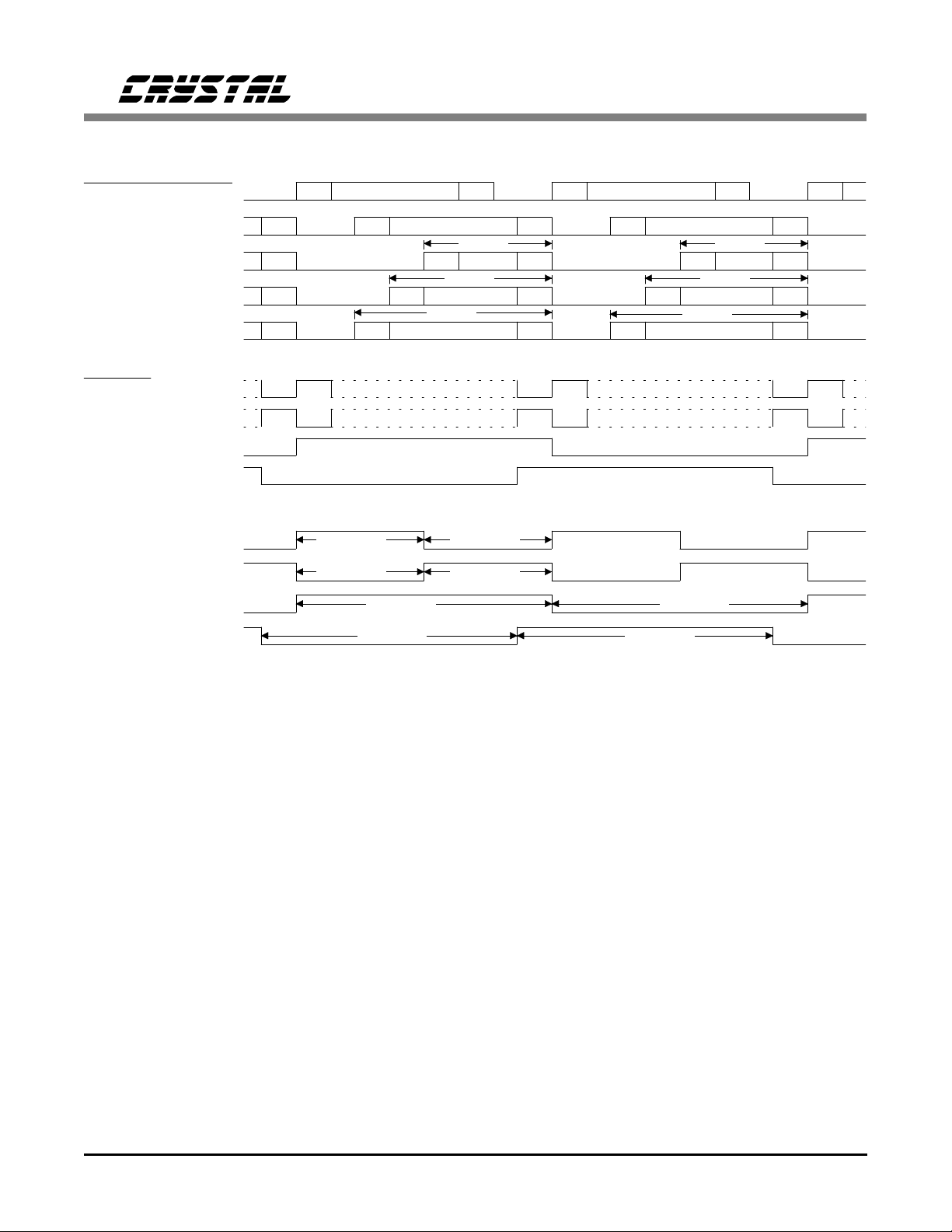
SWITCHING CHARACTERISTICS - SERIAL PORTS
(TA = 25 °C for suffixes ’-CP’ and ’-CS’; TA = -40 to 85 °C for suffixes ’-IP’ and ’-IS’;
Inputs: Logic 0 = GND, logic 1 = VD+; C
Parameter Symbol Min Typ Max Units
SCK Frequency Master Mode Notes 5,6 t
Slave Mode Note 6 12.5 MHz
= 20 pF)
L
sckf
CS8401A CS8402A
IWR×64 Hz
SCK Pulse Width Low Slave Mode Note 6 t
SCK Pulse Width High Slave Mode Note 6 t
SCK rising to FSYNC edge delay Notes 6,7 t
SCK rising to FSYNC edge setup Notes 6,7 t
SDATA valid to SCK rising setup Note 7 t
SCK rising to SDATA hold time Note 7 t
sckl
sckh
sfds
sfs
sss
ssh
25 ns
25 ns
20 ns
20 ns
20 ns
20 ns
C, U, V valid to SCK rising setup CS8402A
non-CD Mode Notes, 7,8 t
css
0ns
SCK rising to C, U, V hold time CS8402A
non-CD mode Notes 7, 8 t
U valid to SBC rising setup CS8402A, CD mode Note 8 t
SBC rising to U hold time CS8402A, CD mode Note 8 t
scs
uss
suh
50 ns
0ns
80 ns
RST Pulse Width CS8402A 150 ns
Notes: 5. The input word rate, IWR, refers to the frequency at which stereo audio input samples are input to
the part. (A stere o pair is two au dio sample s.) Theref ore, in Maste r mode, the re are always
32 SCK periods in one audio sa mple.
6. Master mode is defined as SCK and FSY NC being ou tputs. In Sla ve mode they are inputs . In the
CS8401A, control reg. 3 bit 1, MSTR, se lects mast er. In the CS8402 A, only form at 0 is master.
7. The table ab ove assume s data is outp ut on the fall ing edge and latched on the r ising edge . In both
parts the edge is selectable. The table is defined for the CS8401A with control reg. 3 bit 0, SCED, set to
one, and for the CS 8402A in for mats 4 thro ugh 7. F or the other format s, the table a nd fig ure edg es
must be rever sed (i e. "ris ing" t o "falli ng" an d vice versa) .
8. The diagr ams show SB C rising coi ncident wit h the first rising edge of SCK after FSYNC transi tions.
This is true for all modes except FSF0 & 1 both equal 1 in the CS8401A, and format 4 in the CS8402A.
In these modes SBC is delayed one full SCK period.
FSYNC
t
sfs
SCK
SDATA
t
sfds
t
sss
t
t
sckh
sckl
t
ssh
Serial Input Timing - Slave Mode
4 DS60F1
Page 5
FSYNC
CS8401A CS8402A
CS8402A
non-CD mode
CD mode
SCK
SDATA
C,U,V
SBC
t
sfds
t
sss
t
css
U
t
uss
t
sfs
t
t
t
ssh
sch
suh
t
sckf
Serial Input Timing - Master Mode & C, U, V Port
Audio
Data
Processor
Audio
Data
Processor
or
Micro-
controller
+5V
Clock
5
External
5 k
7
6
8
15
14
16
FSYNC
SCK
SDATA
INT
CS
RD/WR
MCK
CS8401A
VD+
GND
TXP
19
18
20
A0 - A4
17
D0 - D7
TXN
Figure 1. CS8401A Typical Connection Diagram
+5V
0.1 uF
Transmitter
Circuit
See Appendix B
DS60F1 5
Page 6
CS8401A CS8402A
Audio
Data
Processor
Micro-
controller
or
unused
Channel
Status Bits
Control
External
Clock
7
6
8
15
10
11
9
16
MCK
FSYNC
SCK
SDATA
CBL
CS8402A
C
U
V
RST
8 Dedicated C.S. Bits
5
+5V
19
VD+
GND
TRNPT
M2
M1
M0
TXP
TXN
18
24
20
17
23
22
21
0.1 uF
Serial Port
Mode Select
Transmitter
Circuit
See Appendix B
Figure 2. CS8402A Professional & Consumer Modes Typical Connection Diagram
Audio
Data
Processor
Decoder
Subcode
Port
Reset
Control
Channel
Status Bits
Control
7
FSYNC
6
SCK
8
SDATA
9
V
10
SBF
11
U
15
SBC
16
RST
8 Dedicated C.S. Bits
External
Clock
5
MCK
CS8402A
+5V
VD+
GND
M2
M1
M0
TXP
TXN
19
18
20
17
0.1 uF
23
22
21
See Appendix B
Serial Port
Mode Select
Transmitter
Circuit
Figure 3. Consumer CD Submode Typical Connection Diagram
6 DS60F1
Page 7

CS8401A CS8402A
GENERAL DESCRIPTION
The CS8401A/2A are monolithic CMOS circuits
that encode and transmit audio and digital data
according to the AES/EBU, IEC 958 (S/PDIF),
and EIAJ CP-340 interface standards. Both chips
accept audio and control data separately; multiplex and biphase-mark encode the data
internally; and drive it, directly or through a
tran sfo rme r, to a tra nsm iss ion lin e. T he CS8401A
is fully software programmable through a parallel port and contains buffer memory for control
data, while the CS8402A has dedicated pins for
the most important control bits and a serial input
port for the C, U, and V bits.
Familiarity with the AES/EBU and IEC 958
specifications are assumed throughout this data
sheet. Many terms such as channel status, user
data, auxiliary data, professional mode, etc. are
not defined. The Application Note, Overview of
AES/EBU Digital Audio Interface Data Structures, provides an overview of the AES/EBU and
IEC 958 specifications and is included for clarity; however, it is not meant to be a complete
reference, and the complete standards should be
obtained from the Audio Engineering Society or
ANSI for the AES/EBU document, and the International Electrotechnical Commission for the
IEC document.
Line Drivers
CS8401A DESCRIPTION
The CS8401A accepts 16- to 24-bit audio samples
through a configurable serial port, and channel status,
user, and auxiliary data through an 8-bit parallel port.
The parallel port allows access to 32 bytes of internal
memory which is used to store control information
and buffer channel status, user, and auxiliary data.
This data is multip lexed with the audio data from the
serial port, the parity bit is generated, and the bit
stream is biphase-mark encoded and driven through
an RS422 line driver. A block diagram of the
CS8401A is shown in Figure 4. In accordance with
the professional definition of channel status, the
CRCC code (C.S. byte 23) can be internally generated.
Parallel Port
The parallel port accesses one status register, three
control registers, and 28 bytes of dual port buffer
memory. The address bus, and RD/WR line must be
valid w he n CS goes low. If RD/WR is low, the value
on the data bus wi ll be written into the buffer memory at the specified address. If RD/WR is high, the
value in the buffer memory, at the specified address,
is placed on the data bus. The detailed timing for
reading and writing the CS8401A can be found in
the Digital Switching Characteristics table. The
memory space is allocated as shown in Figure 5.
There are three defined buffer memory modes selectable by two bits in control register 2.
The RS422 line drivers for both the CS8401A
and CS8402A are low skew, low impedance, dif-
ferential outputs capable of driving 110 Ω
transmission lines with a 4 volt peak-to-peak signal when configured as shown in Appendix A.
To prevent possible short circuits, both drivers
are set to ground when no master clock (MCK)
is provided. They can also be disabled by reset-
Status and Control Registers
Upon power up the CS8401A control registers
contain all zeros. Therefore, the part is initially
in reset and is muted. One’s must be written to
control register 2, bits RST and MUTE, before
the part will transmit data. The remaining regis-
ters are not initialized on power-up and may
contain random data.
ting the device (RST = low). Appendix A
contains more information on the line drivers. A
0.1 µF capacitor, with short leads, should be
placed as close as possible to the VD+ and GND
pins.
DS60F1 7
The first register, shown in Figure 6, is the status
register in which only three bits are valid. The lower
three bits contain flags indicating the position of the
transmit pointer in the buffer memory. These flags
Page 8
CS8401A
CS
INT
8
6
7
21-24, 1-4
9-13
14
16
15
Interrupt
Control
Read
Address
Generator
Serial
Port
Logic
Control
and Flags
4 X 8
Buffer
Memory
28 X 8
Figure 4. CS8401A Block Diagram
SDATA
SCK
FSYNC
D0-D7
A4-A0
RD/WR
may be used to avoid contention between the
transmit pointer reading the data and the user updating the buffer memory. Besides indicating the
byte location being transmitted, the flags indicate
the block of memory the part is currently addressing, thereby telling the user which block is
free to be written to. Each flag has a corresponding mask bit (control register 1) which, when set,
allows a transition on the flag to generate a pulse
on the interrupt pin. Flag 0 and flag 1 cause interrupts on both edges whereas flag 2 causes an
interrupt only on the rising edge. Timing and
further explanation of the flags can be found in
the buffer memory section.
The two most significant bits of control register 1,
BKST and TRNPT, are used for Transparent Mode
operation of the CS8401A. Transparent Mode is used
for those applications where it is useful to maintain
frame alignment between the received and transmitted
audio data signals. In Transparent Mode
(TRNPT = "1") the MCK, FSYNC, SCK and
SDATA inputs of the CS8401A can be connected to
their corresponding outputs of the CS8411. In Transparent Mode, FSYNC synchronizes the transmitter
and the receiver. The data delay through the CS8401A
Audio
Aux
C Bits
CRC
U Bits
Validity
Preamble
Parity
Mux
Biphase
Mark
Encoder
Timing
Driver
IMCK
Prescaler
5
MCK
Line
20
TXP
TXN
17
is set so that three frame delays occur from the
input of the CS8411 to the output of the
CS8401A. In Transparent Mode, 32 SCK’s are
required per subframe.
Channel status block alignment between the
CS8411 and the CS8401A is accomplished by
setting BKST high at the occurrence of the Flag
2 rising edge of the CS8411. If FSYNC is a
left/right signal, BKST is sampled once per
frame; if FSYNC is a wo rd clock, BKST is sampled once per subframe. A low to high transition
of BKST (based on two successive internal samples) resets the channel status block boundary to
the beginning.
Control register 2, shown in Figure 8, contains
various system level functions. The two most
significant bits, M1 and M0, select the frequency
at the MCK pin as shown in Table 1. As an example, if the audio sample frequency is 44.1 kHz
and M0 and M1 are both zero, MCK would then
be 128× the audio sample rate or 5.6448 MHz. The
next bit (5) in control register 2, V, indicates the validity of the current audio sample. According to the
8 DS60F1
Page 9
digital audio specifications, V = 0 signifies the
audio signal is suitable for conversion to analog.
B1 and B0 select one of three modes for the
buffer memory. The different modes are shown
in Figure 5 and the bit combinations in Table 2.
More information on the different modes can be
found in the Buffer Memory section. Bit 2, CRCE, is
the channel status CRCC enable and should only be
used in professional mode. When CRCE is high, the
0
1
2
3
4
5
6
7
8
1st Four
9
Bytes of
A
C. S. Data
B
C
A
D
D
E
D
F
R
E
S
S
10
11
12
13
14
15
16
17
18
19
1A
1B
1C
1D
1E
1F
20 Bytes
Channel
Figure 5. CS8401A Buffer Memory Modes
Status register 0
Control Register 1
Control Register 2
Control Register 3
User Data
1st Four
Bytes of
C. S. Data
C. S.
Data
Last
Status
Data
Auxiliary
Data
0123
Memory Mode
1st Four
Bytes of
Left C. S.
Data
Left
C. S.
Data
1st Four
Bytes of
Right
C. S. Data
Right
C. S.
Data
U
N
D
E
F
I
N
E
D
CS8401A
X:00
FLAG2: High for first four bytes of channel status
FLAG1: Memory mode dependent - See figure 11
FLAG0: High for last two bytes of user data.
Figure 6. Status Regist er
X:01
BKST: Causes realignment of data block when set to "1".
TRNPT: Selects Transparent Mode appropriately setting data
MASK2: Interrupt mask for FLAG2. A "1" enables the interrupt.
MASK1: Interrupt mask for FLAG1.
MASK0: Interrupt mask for FLAG0.
delay through device
Figure 7. Contro l Re gister 1
X:02
M1: with M0, selects MCK frequency.
M0: with M1, selects MCK frequency.
V: Validity bit of current sample.
B1: with B0, selects the buffer memory mode.
B0: with B1, selects the buffer memory mode.
CRCE: Channel status CRC Enable. Professional mode only.
MUTE: When clear, transmitted audio data is set to zero.
RST: When clear, drivers are disabled, frame counters cleared.
Figure 8. Contro l Re gister 2
M1 M0 MCLK
00128
01192
10256
11384
Input Word Rate
×
Input Word Rate
×
Input Word Rate
×
Input Word Rate
×
Table 1. MCLK Frequencies
B1 B0 Mode Buffer Memory Contents
0 0 0 Channel Status
0 1 1 Auxiliary Da ta
1 0 2 Independent Channel Status
1 1 3 Reserved
Table 2. Buffer Memory Modes
MASK0MASK1MASK2TRNPTBKST
01234567
FLAG0FLAG1FLAG2
01234567
01234567
RSTMUTECRCEM0M1 V B1 B0
DS60F1 9
Page 10
CS8401A
channel status data cyclic redundancy check
characters are generated independently for channels A and B and are transmitted at the end of the
channel status block. When MUTE (bit 1) is low,
the transmitted audio data is forced to zero. Both
RST and MUTE are set to zero upon power up.
When RST is low, the differential line drivers are
set to ground and the block counters are reset to the
beginning of the first block. In order to properly
synchronize the rest of the CS8401A to the audio
serial port, the transmit timing counters, which include the flags in the status register, are not enabled
after RST is set high until eight and one half SCK
periods after the active edge (first edge after reset is
exited) of FSYNC.
When FSYNC is configured as a left/right signal
(FSF1 = 1), the counters and flags are not enabled until the right sample is being entered
(during which the previous left sample is being
transmitted). This guarantees that channel A is
left and Channel B is right as per the digital
audio interface specs.
of the formats delineate each channel’s data and
do not indicate the particular channel. The other
two formats also indicate the specific channel.
The formats are shown in Figure 10. Bit 1,
MSTR, determines whether FSYNC and SCK
are inputs, MSTR low, or outputs, MSTR high.
Bit 0, serial clock edge select, SCED, selects the
edge that audio data gets latched on. When
SCED is low, the falling edge of SCK latches
data in the chip and when SCED is high, the rising edge is used.
The multitude of combinations allow for a zero
glue logic interface to almost all DSP’s, encoder
chips, and standard serial data formats.
Serial Port
The serial port is used to enter audio data and
consists of three pins: SCK, SDATA, and
FSYNC. The serial port is double buffered with
SCK clocking in the data from SDATA, and
FSYNC delineating audio samples and may define the particular channel, left or right.
Control register 3 contains format information for
the serial audio input channel. The MSB is unused
and the next three bits, SDF2-SDF0, select the format for the serial input data with respect to
FSYNC. There are five valid combinations of these
bits as shown in Figure 10. The next two bits,
FSF1 and FSF0, select the format of FSYNC. Two
01234567
X:03
SDF2: with SDF0 & SDF1, select serial data format.
SDF1: with SDF0 & SDF2, select serial data format.
SDF0: with SDF1 & SDF2, select serial data format.
FSF1: with FSF0, select FSYNC format.
FSF0: with FSF1, select FSYNC format.
MSTR: When set, SCK and FSYNC are outputs.
SCED: When set, rising edge of SCK latches data.
When clear, falling edge of SCK latches data.
SDF1
Figure 9. Contro l Re gister 3
SCEDMSTRFSF0SDF2 SDF0 FSF1
Control register 3, shown in Figure 9, configures
the serial port. All the various formats are illustrated in Figure 10. When FSF1 is low, FSYNC
only delineates audio samples. When FSF1 is
high, it delineates audio samples and specifies
the channel. When FSF1 is low and the port is a
master (MSTR = 1), FSYNC is a square wave
output. When FSF1 is low and the port is a slave
(input), FSYNC can be a square wave or a pulse
provided the active edge, as defined in Figure 10, is properly positioned with respect to
SDATA.
Bits 4, 5, and 6, SDF0-SDF2, define the format
of SDATA and is also described in Figure 10.
The five allowable formats are MSB first, MSB
last, 16-bit LSB last, 18-bit LSB last, and 20-bit
LSB last. The MSB first and MSB last formats
accept any word length from 16 to 24 bits. The
word length is controlled by providing trailing
zeros in MSB first mode and leading zeros in
10 DS60F1
Page 11
CS8401A
SDF
210 (bit)
000
001
010
100
110
FSF
10 (bit)
00
01
10
11
00
01
10
Name
MSB First
MSB Last
LSB Last 16
LSB Last 18
LSB Last 20
MSTR
0
FSYNC Input
0
FSYNC Input
0
FSYNC Input
0
FSYNC Input
1
FSYNC Output
1
FSYNC Output
1
FSYNC Output
Left Sample
MSB LSB MSB LSB MSB
MSB LSB MSB LSB MSB
LSB LSBMSB LSBMSB
LSB LSBMSB LSBMSB
LSB
24 bits, incl. Aux 24 bits, incl. Aux
24 bits, incl. Aux 24 bits, incl. Aux
16 Bits
18 Bits
20 Bits
MSB LSB MSB LSB
16 Clocks 16 Clocks
16 Clocks 16 Clocks
32 Clocks 32 Clocks
Right Sample
16 Bits
18 Bits
20 Bits
11
1
FSYNC Output
32 Clocks
Figure 10. CS8401A Serial Port SDATA and FSYNC Timing
MSB last mode, or by restricting the number of
SCK periods between samples to the sample
word length. The 16-, 18-, and 20-bit LSB-last
modes require at least 16, 18, or 20 SCK periods
per sample respectively. As a master, 32 SCK periods are output per sample.
FSYNC must be derived from MCK via a DSP
using the same clock or by external counters. If
FSYNC moves (jitters) with respect to MCK by
more than 4 MCK periods, the CS8401A may
reset the channel status block and flags. Appendix C contains more information on the
relationship of FSYNC and MCK.
Buffer Memory
In all buffer modes, the status register and control registers are located at addresses 0-3
32 Clocks
respectively, and the user data is buffered in locations 4-7. The parallel port can access any
location in the user data buffer at any time; however, care must be taken not to modify a location
when that location is being read internally. This
internal reading is done through the second port
of the buffer and is done in a cyclic manner.
Reset initializes the internal pointer to
04H (Hex). Data is read from this location and
stored in an 8-bit shift register which is shifted
once per audio sample. (An audio sample is defined as a single channel, not a stereo pair.) The
byte is transmitted LSB first, D0 being the first
bit. After transmitting 8 samples, i.e. 8 user bits,
the address pointer is incremented and the next
byte of user data is loaded into the shift register.
After transmitting all four bytes, 32 audio sam-
DS60F1 11
Page 12

CS8401A
ples, the user read pointer is reset to 04H (Hex)
and the cycle repeats.
Flag 0 in the status register monitors the position
of the internal user data read pointer. When the
first byte, location 04H, is read, flag 0 is set low
and when the third byte, location 06H, is read,
flag 0 is set high. If mask 0 in control register 1
is set, a transition of flag 0 will generate a low
pulse on the interrupt pin. The value of flag 0
indicates which two bytes the part will read next,
thereby indicating which two bytes are free to be
updated.
(384 Audio Samples)
Flag 2
Flag 1
Mode 0
Flag 1 is mode dependent, changing with buffer
memory configuration, and is discussed in the
individual buffer mode sections.
Flag 2 is set high when byte 0 of the channel
status, address 08H, is read, and set low when
byte 4, address 0BH, is read. Therefore, flag 2
high indicates the part is reading the first four
bytes of channel status, and the last 20 bytes are
free to update. If the interrupt mask bit for flag 2
is set, the rising edge will cause an interrupt indicating the beginning of a channel status block
as shown in Figure 11. Although a falling edge
Block
Flag 1
Modes 1 & 2
Flag 0
23 0 1 2 3 4 5 6 7 8 91011121314151617181920212223 0 1
Channel Status Byte
(Expanded)
Frame
B 0A 0 A 1 B 1 B 2A 2 B 7A 7
(Expanded)
03478
bit
See figure 15
Sub-frame
Audio Data
28 29 30 3127
VUCPMSBAux Data LSBPreamble
Validity
User Data
Channel Status Data
Parity Bit
Figure 11. CS8401A Status Register Flag Timing
12 DS60F1
Page 13

CS8401A
on flag 0 and flag 1 may cause an interrupt, the
falling edge of flag 2 will not.
Figure 11 illustrates the flag timing for an entire
channel status block which includes 24 bytes of
channel status data and 384 audio samples. (This
figure assumes the channel status bit is the same
for the audio pair.) The lower portion of Figure 11 expands the first byte of channel status
showing eight pairs of data with a pair defined
as a frame. This is further expanded showing the
first sub-frame (A0) to contain 32 bits as per the
AES/EBU specifications (see Appendix A).
When transmitting stereo, channel A is left and
channel B is right. The preamble at the bottom
of Figure 11 is expanded in Figure 15 to show
the exact timing between flags, the interrupt pin,
and internal buffer-read timing.
Buffer Mode 0
reads this buffer in a cyclic non-destructive manner and stores the byte in an 8-bit shift register
that is shifted once per two transmitted audio
samples (once per frame).
Flag 1 in the status register can be used to monitor the channel status buffer. In mode 0, flag 1 is
set low when byte 0, location 08H, is read, and
set high when byte 16, location 18H, is read. If
mask 1 in control register 1 is set, a transition on
flag 1 will generate a pulse on the interrupt pin.
Figure 12 illustrates the memory read sequence
for buffer mode 0 along with the flag timing.
The arrows on the flags indicate an interrupt if
the appropriate mask bit is set. Flag 0 can cause
an interrupt on either edge, which is shown only
in the expanded portion of the Figure for clarity.
The expanded section also shows that the user
buffer is reread when location 0AH of the channel status is read.
In buffer mode 0, in addition to the user-data
buffer previously discussed, one entire block of
channel status data is buffered in 24 memory locations from address 08H to 1FH. This block
will be transmitted in both channel A and channel B, one bit per frame. Like the user-data
buffer, the parallel port can access any location
in this buffer at any time. The transmitter section
(384 Audio Samples)
Flag 2
Flag 1
Flag 0
0 1 2 3 4 5 6 7 8 9 1011121314151617181920212223 0 1C.S. Byte
08 0B 1FC.S. Address
0C 08
(Expanded)
Buffer Mode 1
In buffer mode 1, eight bytes are allocated for
channel status data and 16 bytes for auxiliary
data as shown in Figure 5. The channel status
buffer, locations 08H to 0FH, is divided into two
sections. The first four locations always contain
the first four bytes of channel status, identical to
Block
Flag 0
C.S. Address
User Address
DS60F1 13
08 09 0A 0B
04 05 06 07
Figure 12. CS8401A Buffer Memory Read Sequence - MODE 0
04 05 06 07
(Addresses are in Hex)
Page 14

CS8401A
mode 0, and are read once per channel status
block. The second four locations, addresses 0CH
to 0FH, provide a cyclic buffer for the last 20
bytes of channel status data.
Similar to mode 0, transmitted channel status
data will be the same for channel A and channel B (one channel status bit per frame). Flag 1
and flag 2 can be used to monitor this buffer.
Flag 1 is set low when byte 0 of channel status
data, location 08H, is read and is toggled when
every other byte is read. As shown in Figure 13,
flag 2 is set high when byte 0, location 08H, is
read and set low when byte 4, location 0CH, is
read. Flag 2 determines whether the channel
status pointer is reading the first four-byte section or the second four-byte section, while flag 1
indicates which two bytes of the section are free
to update.
The auxiliary data buffer, locations 10H to 1FH,
is read in a cyclic manner similar to the data
buffer; however, four auxiliary data bits are
transmitted per audio sample (sub-frame). Since
the auxiliary buffer must be read four times as
often as the user data buffer and is four times as
large, flag 0 can be used to monitor both.
Buffer Mode 2
In buffer mode 2, two 8-byte buffers are available for buffering both channel A and channel B
channel status data independently. Both buffers
are identical to the channel status buffer in
mode 1 except that each channel can have
unique channel status data. The two buffers are
read simultaneously with locations 08H to 0FH
transmitted in channel A and locations 10H to
17H transmitted in channel B. Figure 5 contains
the buffer memory modes and Figure 14 illustrates the buffer read sequence for mode 2.
Flag 2
Flag 1
Flag 0
Flag 1
Flag 0
C.S. Address
User Address
Aux. Address
Block
(384 Audio Samples)
0123456789101112131415161718192021222301C.S. Byte
08 0B 0C 0F 08C.S. Address
08 09 0A 0B
04 05 06 07 04 05 06 07
10 13,14 17 18 1B,1C 1F 10 13,14 17 18 1B,1C 1F
Figure 13. CS8401A Buffer Memory Read Sequence - MODE 1
0F 0C 0F 0C 0F 0C 0F 0C
(Expanded)
(Addresses are in Hex)
14 DS60F1
Page 15

Flag 2
Flag 1
Flag 0
Left C.S. Ad.
CS8401A
Block
(384 Audio Samples)
0123456789101112131415161718192021222301C.S. Byte
08 0B 0C 0F 08
10 13 14 14 1017 14 17 14 17 14 17 14Right C.S. Ad.
0F 0C 0F 0C 0F 0C 0F 0C
(Expanded)
Flag 1
Flag 0
Left C.S. Ad.
User Address
08 09 0A 0B
10 11 12 13Right C.S. Ad.
04
05 06 07
Figure 14. CS8401A Buffer Memory Read Sequence - MODE 2
04 05 06 07
Buffer-Read and Interrupt Timing
As mentioned previously in the buffer mode sections, conflicts between externally writing to the
buffer ram and the CS8401A internally reading
bytes of ram for transmission may be averted by
using the flag levels to avoid the section currently being addressed by the part. Interrupts
occur at flag edges indicating the exact byte that
the part is currently reading. Utilizing INT along
with the flags, the byte currently being read by the
part can be avoided allowing access to all other
bytes instead of just a section. Figure 15 ill ustr ates
the timing between flags, INT, and the internal
(Addresses are in Hex)
reading of the buffer for transmission. The master clock IMCK is shown as 128×Fs. Other
MCK frequencies are initially divided to obtain
128×Fs, defined as IMCK (internal MCK),
which is then used for all internal timing, so the
timing in Figure 15 is valid for all MCK frequencies. When the parity bit (P) is transmitted, a
transition on a flag causes INT to go low if the
appropriate mask bit is set. Concurrently, the part
starts reading from the internal buffer. Writing to
the buffer ram location being read by the part
should be avoided while the internal "ram read"
signal is high.
IMCK
(128Fs)
Flags 0 & 1
Flag 2
INT
RAM Read
TXP
TXN
Figure 15. RAM/Buffer-Read and Interrupt Timing
DS60F1 15
PC
Transmit Preamble
Page 16

PIN DESCRIPTIONS
DATA BUS BIT 4 D4 D3 DATA BUS BIT 3
DATA BUS BIT 5 D5 D2 DATA BUS BIT 2
DATA BUS BIT 6 D6 D1 DATA BUS BIT 1
DATA BUS BIT 7 D7 D0 DATA BUS BIT 0
MASTER CLOCK MCK TXP TRANSMIT POSITIVE
SERIAL DATA CLOCK SCK VD+ PO WER
FRAME SYNC FSYNC GND GROUND
SERIAL INPUT DATA SDATA TXN TRANSMIT NEGATIVE
ADDRESS BUS BIT 4 A4 RD/
ADDRESS BUS BIT 3 A3
ADDRESS BUS BIT 2 A2
ADDRESS BUS BIT 1 A1 A0 ADDRESS BUS BIT 0
Power Supply Connections
VD+ - Positive Digital Power, PIN 19.
Positive supply for the digital section. Nominally +5 volts.
CS8401A
1
24
2
23
3
22
4
21
5
20
6
19
7
18
8
17
9
16
10
15
11
14
12 13
CS8401A
WR READ/WRITE SELECT
INT INTERRUPT
CS CHIP SELECT
GND - Ground, PIN 18.
Ground for the digital section.
Audio Input Interface
SCK - Serial Clock, PIN 6.
Serial clock for SDATA pin which can be configured (via control register 3) as an input or
output, and can sample data on the rising or falling edge. As an output, SCK will contain 32
clocks for every audio sample. As an input, it does not need to be continuous and can be up to
15 MHz.
FSYNC - Frame Sync, PIN 7.
Delineates the serial data and may indicate the particular channel, left or right. Also, FSYNC
may be configured as an input or output. The format is based on bits in control register 3.
SDATA - Serial Data, PIN 8.
Audio data serial input pin.
Parallel Interface
CS - Chip Select, PIN 14.
This input is active low and allows access to the 32 bytes of internal memory. The address bus
and RD/WR must be valid while CS is low.
16 DS60F1
Page 17

RD/WR - Read/Write, PIN 16.
If RD/WR is low when CS goes active (low), the data on the data bus is written to internal
memory. If RD/WR is high when CS goes active, the data in the internal memory is placed on
the data bus.
A4-A0 - Address Bus, PINS 9-13.
Parallel port address bus that selects the internal memory location to be read from or written to.
D0-D7 - Data Bus, PINS 21-24, 1-4.
Parallel port data bus used to check status, write control words, or write internal buffer memory.
INT - Interrupt, PIN 15.
Open drain output that can signal the state of the internal buffer memory. A 5kΩ resistor to
VD+ is typically used to support logic gates. All bits affecting INT are maskable allowing total
control over the interrupt mechanism.
Transmitter Interface
MCK - Master Clock, PIN 5.
Clock input which defines the transmit timing. It can be configured, via control register 2, for
128, 192, 256, or 384 times the sample rate.
CS8401A
TXP, TXN - Differential Line Drivers, PINS 20, 17.
RS422 compatible line drivers. Drivers are pulled low when part is in reset state.
DS60F1 17
Page 18

CS8402A
CS8402A DESCRIPTION
The CS8402A accepts 16- to 24-bit audio samples
through a serial port configured in one of seven formats; provides several pins dedicated to particular
channel status bits; and allows all channel status,
user, and validity bits to be serially input through
port pins. This data is multiplexed, the parity bit is
generated, and the bit stream is biphase-mark encoded and driven through an RS422 line driver.
The CS8402A operates as a professional or consumer interface transmitter selectable by pin 2,
PRO. As a professional interface device, the dedicated channel status input pins are defined according
to the professional standard, and the CRC code (C.S.
byte 23) can be internally generated.
As a consumer device, the dedicated channel
status input pins are defined according to the
consumer standard. A submode provided under
the consumer mode is compact disk, CD, mode.
When transmitting data from a compact disk, the
CD subcode port can accept CD subcode data,
extract channel status information from it, and
transmit it as user data.
The master clock, MCK, controls timing for the entire chip and must be 128×Fs. As an example, if
stereo data is input to the CS8402A at 44.1 kHz,
MCK input must be 128 times that or 5.6448 MHz.
with the I2S standard. Formats 5 and 6 make
the CS8402A look similar to existing 16- and
18-bit DACs, and interpolation filters. Format 7 is an MSB-last format and is conducive
to serial arithmetic. SCK and FSYNC are
outputs in Format 0 and inputs in all other
formats. In Format 2, the rising edge of
FSYNC delineates samples and the falling
edge must occur a minimum of one bit period
before or after the rising edge. In all formats
except 2, FSYNC contains left/right information requiring both edges of FSYNC to
delineate samples. Formats 5 and 6 require a
minimum of 16- or 18-bit audio words respectively. In all formats other than 5 and 6,
the CS8402A can accept any word length
from 16 to 24 bits by adding leading zeros in
format 7 and trailing zeros in the other formats, or by restricting the number of SCK
periods between active edges of FSYNC to
the sample word length.
FSYNC must be derived from MCK, either
through a DSP using the same clock, or using
counters. If FSYNC moves (jitters) with respect
to MCK by four MCK periods, the internal
counters and CBL may be reset. Appendix B
contains more information on the relationship
between FSYNC and MCK.
Audio Serial Port
The audio serial port is used to enter audio data
and consist of three pins: SCK, SDATA, and
FSYNC. SCK clocks in SDATA, which is double
buffered, while FSYNC delineates the audio samples and may indicate the particular channel, left or
right. To support many different interfaces, M2,
M1, and M0 select one of seven different formats
for the serial port. The coding is shown in Table 3
while the formats are shown in Figure 16. Format 0
and 1 are designed to interface with Crystal ADCs.
M2 M1 M0 Format
0 0 0 0 - FSYNC & SCK Output
0 0 1 1 - Left/Right, 16-24 Bits
0 1 0 2 - Word Sync, 16-24 Bits
0113 - Reserved
1 0 0 4 - Left/Ri ght, I2S Compatible
1 0 1 5 - LSB Justified, 16 Bits
1 1 0 6 - LSB Justified, 18 Bits
1 1 1 7 - MSB Last, 16-24 Bits
Format 2 communicates with Motorola and TI
DSPs. Format 3 is reserved. Format 4 is compatible
18 DS60F1
Table 3. CS8402A Audio Port Modes
Page 19

CS8402A
FORMAT 0:
FORMAT 1:
FORMAT 2:
FORMAT 3:
FORMAT 4:
FSYNC (out)
SCK (out)
SDATA (in)
FSYNC (in)
SCK (in)
SDATA (in)
FSYNC (in)
SCK (in)
SDATA (in)
(RESERVED)
FSYNC (in)
Left Right
MSB LSB MSB LSB MSB
Left Right
MSB LSB MSB LSB MSB
Left
MSB LSB MSB LSB MSB
Left Right
Right
FORMAT 5:
FORMAT 6:
FORMAT 7:
SCK (in)
SDATA (in)
FSYNC (in)
SCK (in)
SDATA (in)
FSYNC (in)
SCK (in)
SDATA (in)
FSYNC (in)
SCK (in)
SDATA (in)
Arrows indicate where C, U, and V bits are latched
LSB
LSB
MSB
Figure 16. CS8402A Audio Serial Port Formats
MSB LSB MSB LSB
Left Right
MSB LSB MSB LSB
16 Bits 16 Bits
Left Right
MSB LSB MSB LSB
Left Right
LSB MSB LSB MSB
MSB
18 Bits18 Bits
DS60F1 19
Page 20

CS8402A
C, U, V Serial Port
The serial input pins for channel status (C), user
(U), and validity (V) are sampled during the first
bit period after the active edge of FSYNC for all
formats except Format 4, which is sampled during the second bit period (coincident with the
MSB). In Figure 16, the arrows on SCK indicate
when the C, U, and V bits are sampled. The C,
U, and V bits are transmitted with the audio
sample entered before the FSYNC edge that
sampled it. The V bit, as defined in the audio
standards, is set to zero to indicate the audio data
is suitable for conversion to analog. Therefore,
when the audio data is errorred, or the data is
not audio, the V bit should be set high. The
channel status serial input pin (C) is not available in consumer mode when the CD subcode
port is enabled (FC1 = FC0 = high). Any channel status data entered through the channel status
serial input (C) is logically OR’ed with the data
entered through the dedicated pins or internally
generated.
RST and CBL (TRNPT is low)
When RST goes low, the differential line drivers
are set to ground and the block counters are reset
to the beginning of the first block. In order to
properly synchronize the CS8402A to the audio
serial port, the transmit timing counters, which
include CBL, are not enabled after RST goes
high until eight and one half SCK periods after
the active edge (first edge after reset is exited) of
FSYNC. When FSYNC is configured as a
left/right signal (all defined formats except 2),
the counters and CBL are not enabled until the
right sample is being entered (during which the
previous left sample is being transmitted). This
guarantees that channel A is left and channel B
is right as per the digital audio interface specs.
As shown in Figure 17, CBL, channel block start
output, can assist in serially inputting the C, U
and V bits as CBL goes high one bit period before the first bit of the preamble of the first
sub-frame of the channel status block is trans-
TRNPT high
CBL
TRNPT low
SDATA
FSYNC
TRNPT high
C,U,V
TRNPT low
TXP
TXN
Left 0 Left 1Right 0 Right 0Right 128 Left 0Left 128
C bits from Cpin
CUV0L CUV0R CUVIL
CUV191R CUV0L CUV0R
C bits OR'ed w/
PRO pin
Right 191
VUCP191R
Preamble Y
0347
Aux Data
Left 0
VUCP0L
Preamble Z
8
LSB
C bit OR'ed w/
C1 pin
Right 0
VUCP0R
Preamble Y
Left 0 - Audio DataPreamble Z
Sub-frame
CUV1R
CUV1L
VUCP127R
CUV128R
CUV128L
Bit 0 of C.S.
Block Byte 16
Left 128
VUCP128L
Preamble X
MSB
CUV0L CUV0R
CUV191R CUV0L
Right 128
Preamble Y
28 29 30 31
27bit
V0 P0C0U0
Figure 17. CBL and Transmitter Timing
20 DS60F1
Page 21

CS8402A
mitted. This sub-frame contains channel status
byte 0, bit 0. CBL returns low one bit period before the start of the frame that contains bit 0 of
channel status byte 16. CBL is the exact inverse
of flag 1 in mode 0 on the CS8401 (see Figure 11). CBL is not available when the CD
subcode port is enabled.
Figure 17 illustrates timing for stereo data input
on the audio port. Notice how CBL rises while
the right channel data (Right 0) is input, but the
previous left channel data (Left 0) is being transmitted as the first sub-frame of the channel
status block (starting with preamble Z). The C,
U, and V input ports only need to be valid for a
short period after FSYNC changes. A sub-frame
includes one audio sample while a frame includes a stereo pair. A channel status (C.S.)
block contains 24 bytes of channel status and
384 audio samples (or 192 stereo pairs, or
frames, of samples).
Figure 17 shows the CUV ports as having left
and right bits (e.g. CUV0L, CUV0R). Since the
C.S. block is defined as 192 bits, or one bit per
frame, there are actually 2 C.S. blocks, one for
channel A (left) and one for channel B (right).
When inputting stereo audio data, both blocks
normally contain the same information, so C0L
and C0R from the input port pin are both channel status bit 0 of byte 0, which is defined as
professional/consumer. These first two bits from
the port, C0L and C0R, are logically OR’ed with
the inverse of PRO, since PRO is a dedicated
channel status pin defined as C.S. bit 0. Also, if
in professional mode, C1, C6, C7 and C9 are
dedicated C.S. pins. The inverse of C1 is logically OR’ed with channel status input port bits
C1L and C1R. In similar fashion, C6, C7 and C9
are OR’ed with their respective input bits. Also,
the C bits in CUV128L and CUV128R are both
channel status block bit 128, which is bit 0 of
channel status byte 16.
Transparent Mode
In certain applications it is desirable to receive
digital audio data with the CS8412 and retransmit it with the CS8402A. In this case, channel
status, user and validity information must pass
through unaltered. For studio environments, AES
recommends that signal timing synchronization
be maintained throughout the studio. Frame synchronization of digital audio signals input to and
output from a piece of equipment mu st be within
±5%.
The transparent mode of the CS8402A is selected by setting TRNPT, pin 24, high. In this
mode, the CBL pin becomes an input, allowing
direct connection of the outputs of the CS8412
to the inputs of the CS8402A as shown in Figure 18. The transmitter and receiver are
synchronized by the FSYNC signal. CBL specifies the start of a new channel status block
boundary, allowing the transmit block structure
to be slaved to the block structure of the receiver. In the transparent mode, C, U, and V are
now transmitted with the current audio sample as
shown in Figure 17 (TRNPT high), and the dedicated channel status pins are ignored. When in
the transparent mode, the propagation delay of
data through the CS8402A is set so that the total
propagation delay from the receive inputs of the
CS8412 to the transmit outputs of the CS8402A
is three frames.
V+
TXP
TXN
RXP
RXN
CS8412
MCK
CBL
C
U
V
FSYNC
SCK
SDATA
Data
Processing
TRNPT
CS8402A
Figure 18. Transparent Mode Interface
DS60F1 21
Page 22

CS8402A
When FSYNC is a word clock (Format 2), CBL
is sampled when left C,U,V are sampled. When
FSYNC is Left/R ight, CBL is sampled when left
C,U,V are sampled. The channel status block
boundary is reset when CBL transitions from
low to high (based on two successive samples of
CBL). MCK for the CS8402A is normally expected to be 128 times the sample frequency, in
the transparent mode MCK must be 256 Fs.
Professional Mode
Setting PRO low places the CS8402A in professional mode as shown in Figure 19. In
professional mode, channel status bit 0 is transmitted as a one and bits 1, 2, 3, 4, 6, 7, and 9
can be controlled via dedicated pins. The pins
are actually the inverse of the identified bit. For
example, tying the C1 pin low places a one in
channel status bit 1. As shown in the Application
Note, Overview of AES/EBU Digital Audio Interface Data Structures, C1 indicates
audio/non-audio; C6 and C7 determine the sample frequency; and C9 allows the encoded
channel mode to be stereophonic. EM1 and EM0
determine emphasis and encode C2, C3, C4 as
shown in Table 4. The dedicated channel status
pins are read at the appropriate time and are
logically OR’ed with data input on the channel
status port, C. In Transparent Mode, these dedicated channel status pins are ignored; and
channel status bits are input at the C pin.
The channel status data cyclic redundancy check
character (C.S. byte 23) is always generated independently for channels A and B and is
transmitted at the end of the channel status
block.
Data should not be input through the channel status
port, C, during the CRCC byte time frame, since inputs on C are logically OR’ed with internally
generated data.
Consumer Mode
Setting P RO high places the CS8402A in consumer
mode which redefines the pins as shown in Figure 20. In consumer mode, channel status bit 0 is
transmitted as a zero and channel status bits 2, 3, 8,
9, 15, 24, and 25 are controlled via dedicated pins.
The pins are actually the inverse of the bit so if pin
SDATA
SCK
FSYNC
TRNPT
M2 M1 M0
8
6
7
10
C
11
U
9
V
24
Registers
142
EM0
13
EM1
23 22 21
Serial
Port
Logic
12143
C9C7C6C1PRO
Audio
Aux
C Bits
CRC
U Bits
Validity
Preamble
Parity
Mux
Biphase
Mark
Encoder
Timing
15
CBL
5
MCK
Line
Driver
16
20
TXP
TXN
17
RST
Figure 19. CS8402A Block Diagram - Professional Mode
22 DS60F1
Page 23

CS8402A
C2 is tied high, channel status bit 2 will be transmitted as a zero. Also, FC0 and FC1 are encoded
versions of channel status bits 24 and 25, which
define the sample frequency. When FC0 and FC1
are both high, the part is placed in a CD submode which activates the CD subcode port. This
submode is described in detail in the next section. Table 5 describes the encoding of C24 and
C25 through the FC1 and FC0 pins. According
to AES/EBU standards, C2 is copy prohibit/permit, C3 specifies pre-emphasis, C8 and C9
define the category code, and C15 identifies the
generation status of the transmitted material (i.e..
first generation, second generation).
Consumer - CD Sub mode
The consumer CD submode is invoked by placing the part in consumer mode (PRO = high) and
EM1 EM0 C2 C3 C4
00111
01110
10100
11000
setting both FC1 and FC0 high. This mode redefines some of the pins for a CD subcode port as
shown in Figure 21. The CD subcode port pins,
SBF and SBC, replace the C and CB L pins respectively. The user data input, U, becomes the CD
subcode input. Figure 22 describes the timing for
the CD subcode port. When SBF is low, SBC becomes active, clocking in the subcode bits. SBF
goes high for one SCK period, one half SCK period after the active edge of FSYNC for all formats
(except format 4, which will be one and a half
SCK periods after the active edge of FSYNC). SBF
high for more than 16 SBC periods indicates the
start of a subcode block. The first, third, and fourth
Q bits after the start of a subcode block become
channel status bits 5, 2, and 3 respectively. Channel status bits are set by the dedicated pins; the
category code is forced to CD.
FC1 FC0 C2 4 C25 Comments
00 0044.1 kHz
01 0148.0 kHz
10 1132.0 kHz
1 1 0 0 44.1 kHz, C D Mode
SDATA
SCK
FSYNC
+5V
Table 4. Emphasis Encoding
M2 M1 M0
8
6
7
10
C
11
U
9
V
Registers
32
FC1
FC0
24
23 22 21
Serial
Port
Logic
Preamble
141314
12
C9C8C3C2PRO
Figure 20. CS8402A Block Diagram - Consumer Mode
C15
Table 5. Sample Frequency Encoding
Audio
Aux
Biphase
C Bits
U Bits
Validity
Parity
Mux
Mark
Encoder
Timing
15
CBL
MCK
20
16
TXP
TXN
17
RST
Line
Driver
5
DS60F1 23
Page 24

SDATA
SCK
FSYNC
SBF
SBC
CS8402A
M2 M1 M0
23 22 21
8
6
7
10
11
U
15
Serial
Port
Logic
Subcode
Port
Audio
Aux
C Bits
U Bits
Mux
Biphase
Mark
Encoder
Line
Driver
20
TXP
TXN
17
+5V
V
SBF
SBC
16
RST
32
FC1
Register
24
12141314
C15C9C8C3C2PRO
9
FC0
Validity
Preamble
Parity
Timing
5
MCK
Figure 21. CS8402 A Block Diagram - Consumer Mode, CD Submode
U
(Expanded)
SBF
SBC
U
PRSTUVWQ
Data latched on rising edge
Figure 22. CD Subcode Port Timing
24 DS60F1
Page 25

CS8402A
PIN DESCRIPTIONS
CS8402A
1
2
3
4
5
6
7
8
9
10
11
12 13
24
23
22
21
20
19
18
17
16
RST MASTER RESET
15
14
C9 EMPHASIS 0 / CS BIT 9
CS BIT 7 / CS BIT 3
PROFESSIONAL MODE
CS BIT 1 / FREQ. CTRL. 0
CS BIT 6 / CS BIT 2
C7/C3 TRNPT/FC1 TRANSPARENT / FREQ . CTRL 1
PRO M2 SE RIAL PORT MODE SELECT 2
C1/FC0 M1 SERIAL PORT MODE SELECT 1
C6/C2 M0 SERIAL PORT MODE SELECT 0
MASTER CLOCK MCK TXP TRANSMIT POSITIVE
SERIAL DATA CLOCK SCK VD+ POWER
FRAME SYNC FSYNC GND GROUND
SERIAL INPUT DATA SDATA TXN TRA NSMIT NE GATIVE
VALIDITY INPUT V
CS SERIAL IN / SC FRAME CLOCK C/SBF CBL/SBC CS BLOCK OUT / SC BIT CLOCK
USER DATA INPUT UEM0/
CS BIT 9 / CS BIT 15
C9/C15 EM1/C8 EMPHASIS 1 / CS BIT 8
Power Supply Connections
VD+ - Positive Digital Power, PIN 19.
Positive supply for the digital section. Nominally +5 volts.
GND - Ground, PIN 18.
Ground for the digital section.
Audio Input Interface
SCK - Serial Clock, PIN 6.
Serial clock for SDATA pin which can be configured (via the M0, M1, and M2 pins) as an
input or output, and can sample data on the rising or falling edge. As an output, SCK will
contain 32 clocks for every audio sample. As an input, it does not need to be continuous and
can be up to 15 MHz.
FSYNC - Frame Sync, PIN 7.
Delineates the serial data and may indicate the particular channel, left or right, and may be an
input or output. The format is based on M0, M1, and M2 pins.
SDATA - Serial Data, PIN 8.
Audio data serial input pin.
M0, M1, M2 - Serial Port Mode Select, PINS 21, 22, 23.
Selects the format of FSYNC and the samp le edge of SCK with respect to SDATA.
Control Pins
RST - Master Reset, PIN 16.
When low, all internal counters are reset and the line drivers are disabled, pulling low.
DS60F1 25
Page 26

V - Validity, PIN 9.
Validity bit serial input port. This bit is defined according to the digital audio standards wherein
V = 0 signifies the audio signal is suitable for conversion to analog. V = 1 signifies the audio
signal is not suitable for conversion to analog, i.e. invalid. V is sampled once per subframe
U - User Bit, PIN 11.
User bit serial input port is sampled once per subframe.
PRO - Professional/Consumer Select, PIN 2.
Selects between professional mode (PRO low) and consumer mode (PRO high). This pin
defines the functionality of the next seven pins. PRO must be low for Transparent Mode, but
will have no effect on the channel status bits.
C9/C15 - Channel Status Bit 9 / Channel Status Bit 15, PIN 12.
In professional mode, C9 is the inverse of channel status bit 9 (bit 1 of byte 1). In consumer
mode, C15 is the inverse of channel status bit 15 (bit 7 of byte 1). C9/C15 are ignored in
Transparent Mode.
EM0/C9 - Emphasis 0 / Channel Status Bit 9, PIN 14.
In professional mode, EM0 and EM1 encode channel status bits 2, 3, and 4. In consumer mode,
C9 is the inverse of channel status bit 9 (bit 1 or byte 1). EMO/C9 are ignored in Transparent
Mode.
CS8402A
EM1/C8 - Emphasis 1 / Channel Status Bit 8, PIN 13.
In professional mode, EM0 and EM1 encode channel status bits 2, 3, and 4. In consumer mode,
C8 is the inverse of channel status bit 8 (bit 0 of byte 1). EM1/C8 are ignored in Transparent
Mode.
C7/C3 - Channel Status Bit 7 / Channel Status Bit 3, PIN 1.
In professional mode, C7 is the inverse of channel status bit 7. In consumer mode, C3 is the
inverse of channel status bit 3. C7/C3 are ignored in Transparent Mode.
C6/C2 - Channel Status Bit 6 / Channel Status Bit 2, PIN 4.
In professional mode, C6 is the inverse of channel status bit 6. In consumer mode, C2 is the
inverse of channel status bit 2. C6/C2 are ignored in Transparent Mode.
C1/FC0 - Channel Status Bit 1 / Frequency Control 0, PIN 3.
In professional mode, C1 is the inverse of channel status bit 1. In consumer mode, FC0 and
FC1 are encoded versions of channel status bits 24 and 25 (bits 0 and 1 of byte 3). When FC0
and FC1 are both high, CD mode is selected. C1/FC0 are ignored in Transparent Mode.
26 DS60F1
Page 27

TRNPT/FC1 - Transparent Mode / Frequency Control 1, PIN 24.
In professional mode, setting TRNPT low selects normal operation & CBL is an output. Setting
TRNPT high, allows the CS8402A to be connected directly to a CS8412. In transparent mode,
CBL is an input & MCK must be at 256 Fs.
In consumer mode, FC0 and FC1 are encoded versions of channel status bits 24 and 25. When
FC0 and FC1 are both high, CD mode is selected.
C/SBF - Channel Status Serial Input / Subcode Frame Clock, PIN 10.
In professional and consumer modes this pin is the channel status serial input port. In CD mode
this pin inputs the CD subcode frame clock.
CBL/SBC - Channel Status Block Output / Subcode Bit Clock, PIN 15.
In professional and consumer modes, the channel status block output is high for the first 16
bytes of channel status. In CD mode, this pin outputs the subcode bit clock.
Transmitter Interface
MCK - Master Clock, PIN 5.
Clock input at 128× Fs the sample frequency which defines the transmit timing. In transparent
mode, MCK must be 256× Fs.
CS8402A
TXP, TXN - Differential Line Drivers, PINS 20, 17.
RS422 compatible line drivers. Drivers are pulled to low when part is in reset state.
DS60F1 27
Page 28

CS8401A CS8402A
Appendix A: RS422 Driver Information
The RS422 drivers on the CS8401A and CS8402A
are designed to drive both the professional and consumer interfaces. The AES/EBU specification for
professional/broadcast use calls for a 110Ω source
impedance and a balanced drive capability. Since the
transmitter impedance is very low, a 110Ω resistor
should be placed in series with one of the transmit
pins. (A 110Ω resistor in parallel with the transformer would, with the receiver impedance of 110Ω,
provide a 55Ω load to the part which is too low.)
The specifications call for a balanced output drive of
2-7 volts peak-to-peak into a 110Ω load with no ca-
ble attached. Using the circuit in Figure A1, the
output of the transformer is short-circuit protected,
has the proper source impedance, and provides a
5 volt peak-to-peak signal into a 110Ω load. Lastly,
the two output pins should be attached to an XLR
connector with male pins and a female shell, and
with pin 1 of the connector grounded.
CS8401/2A
TXP
TTL or
TXN
Figure A3. TTL/CMOS Output Circuit
CMOS Gate
shown in Figure A2 only uses the TXP pin and
provides the proper output impedance and drive
level using standard 1% resistors. The connector
for consumer would be an RCA phono socket.
This circuit is also short circuit protected.
The TXP pin may be used to drive TTL or
CMOS gates as shown in Figure A3. This circuit
may be used for optical connectors for digital
audio since they are usually TTL compatible.
This circuit is also useful when driving multiple
digital audio outputs since RS422 line drivers
have TTL interfaces.
CS8401/2A
TXP
TXN
Figure A1. Professional Output Circuit
110
XLR
1
In the case of consumer use, the specifications
call for an unbalanced drive circuit with an out-
put impedance of 75Ω and a output drive level
of 0.5 volts peak-to-peak ±20% when measured
across a 75Ω load using no cable. The circuit
CS8401/2A
TXP
TXN
Figure A2. Consumer Output Circuit
374
90.9
RCA
Phono
The transformer should be capable of operating
from 1.5 to 7 MHz, which is the audio data rate
of 25 kHz to 55 kHz after biphase-mark encoding. Transformers provide isolation from ground
loops, 60 Hz noise, and common mode noise
and interference. One of the important considerations when choosing transformers is minimizing
shunt capacitance between primary and secondary windings. The higher the shunt capacitance,
the lower the isolation between primary and secondary, and the more coupling of high frequency
energy. This energy appears in the form of common mode noise on the receive side ground and
has the potential to degrade analog performance.
Therefore, for best performance, shielded transformers optimized for minimum shunt
capacitance should be used. The following are a
few typical transformers:
Pulse Engineering
Telecom Products Group
7250 Convoy Ct.
San Diego, CA 92111
28 DS60F1
Page 29

CS8401A CS8402A
(619) 268-2400
Part Number: PE65612
Schott Corporation
1000 Parkers Lane Rd.
Wayzata, MN 55391
(612) 475-1173
FAX (612) 475-1786
Part N umbe r:
67125450 - compatible with Pulse
67128990 - lower cost
67129000 - surface mount
67129600 - single shield
Scientific Conversions Inc.
42 Truman Drive
Novato, CA. 94947
(415) 8922323
Part N umbe r:
SC916-01 - single shield
SC916-02 - surface mount
Appendix B: MCK and FSYNC Relationship
FSYNC should be derived either directly or indirectly from MCK. The indirect case could be a
DSP, providing FSYNC through its serial port,
using the same master oscillator that generates
MCK. In either case, FSYNC’s relationship to
MCK is fixed and does not move. Since this appendix provides information on what would
happen if FSYNC did move with respect to
MCK, it does not apply to the majority of users.
SDATA
SCK
internally generated
P C U V
CS8402A C,U,V Port
CS8401A Internal
Memory
R1 - Shift (in) Register
R2 - Audio Buffer
All internal ti ming is derived from MCK. On th e
CS8402A, MCK is always 128×Fs. On the
CS8401A, the external MCK is programmable
and is initially divided to 128×Fs before being
used by the part. The internal clock IMCK used
in the following discussion is always 128×Fs re-
gardless of the external MCK pin.
After RST, the CS8401A and CS8402A synchronize the internal timing to the audio data
port, more specifically FSYNC, to guarantee that
channel A is left channel data and channel B is
right channel data as per the AES/EBU specification. If FSYNC moves with respect to IMCK,
the transmitter could lose synchronization, which
causes an internal reset.
Figure B1 shows the structure of the serial port
input, to the transmitter output. The audio data is
serially shifted into R1. PLD is an internal signal
that parallel loads R1 into the R2 buffer, and, at
the same time, the C, U, and V bits are latched.
On the CS8401A, the C, U, and V bits are held
in RAM, whereas on the CS8402A, they are
latched from external pins. The PLD signal rises
on the first SCK edge that can latch data. This is
coincident with the latching of the MSB of audio
data in MSB-first, left-justified modes. PLD
stays high for one SCK period. In the CS8402A
section, the arrows on SCK in Figure 16 indicate
when PLD goes high. Also, SBC in the
CS8402A CD submode is an external version of
PLD gated by the SBF input.
PLD (load signal)
+V
D
LDS (load signal)
Q
Internal Reset
IMCK
2
Figure B1. Serial Port-t o-Transmitter Blo ck Diagram
DS60F1 29
R3 - Shift (out) Register
Preamble
Mux
Biphase
Encode
Driver
TXP
TXN
Page 30

SCK
FSYNC
CS8401A CS8402A
9.5 8.5
SDATA
CS8402A C,U, V
PLD
IMCK
LDS
TXP
TXN
CS8401A Flags
CS8402A CBL
Left 191
CUV191R
VUCP
191L
Figure B2. Serial Ports-to-Transmitter Timing (slave mode)
Preamb.
Left 0
When the part is finished transmitting the preamble of a sub-frame, the internal signal LDS rises
to parallel-load R2 into R3 for transmission. After RST, the part synchronizes the audio port to
IMCK as shown in Figure B2. Since PLD is
based on FSYNC and LDS is based on IMCK, if
Right 0
CUV0L
Right 191
VUCP
191R
Preamb.
Left 0
FSYNC moves with respect to IMCK until PLD
and LDS occur at the same time, the data would
not be properly loaded into R3. If LDS and PLD
overlap, an internal reset is initiated causing the
timing to return to the initial state shown in Figure B2.
Ordering Guide
Model Temperature Range Package
CS8401A-CP 0 to 70 °C* 24-Pin Plastic .3" DIP
CS8401A-IP -40 to 85 °C 24-Pin Plastic .3" DIP
CS8401A-CS 0 to 70 °C* 24-Pin Plastic SOIC
CS8401A-IS -40 to 85 °C 24-Pin Plastic SOIC
CS8402A-CP 0 to 70 °C* 24-Pin Plastic .3" DIP
CS8402A-IP -40 to 85 °C 24-Pin Plastic .3" DIP
CS8402A-CS 0 to 70 °C* 24-Pin Plastic SOIC
CS8402A-IS -40 to 85 °C 24-Pin Plastic SOIC
* Although the ’-CP’ and ’-CS’ suffixed parts are guaranteed to operate over 0 to 70 °C, they are
tested at 25 °C only. If testing over temperature is desired, the ’-IP’ and ’-IS’ suffixed parts are
tested over their specified temperature range.
30 DS60F1
Page 31

L
24 pin
Plastic
Skinny DIP
eA
C
∝∝
SEATING
PLANE
24 13
1
D
B1
e1
12
E1
A
A1
B
NOTES:
1. POSITIONAL TOLERANCE OF LEADS SHALL BE WITHIN
0.25mm (0.010") AT MAXIMUM MATERIAL CONDITION, IN
RELATION TO SEATING PLANE AND EACH OTHER.
2. DIMENSION eA TO CENTER OF LEADS WHEN FORMED PARALLEL.
3. DIMENSION E1 DOES NOT INCLUDE MOLD FLASH.
MILLIMETERS
DIM MIN MAX
A
A1
B
B1
C
D
31.37
E1
e1
eA
L
∝∝
3.94
0.51
0.36
1.02
0.20
6.10
2.41
7.62
3.18
0°
NOM
4.32
0.76
0.46
1.27
0.25
31.75
6.35
2.54
-
-
-
4.57
1.02
0.56
1.65
0.38
32.13
6.60
2.67 0.105
8.25 0.325
3.81
15°
MIN
0.155
0.020
0.014
0.040
0.008
1.235
0.240
0.095
0.300
0.125
0°
INCHES
NOM
0.170
0.030
0.018
0.050
0.010
1.250
0.250
0.100
-
-
-
MAX
0.180
0.040
0.022
0.065
0.015
1.265
0.260
0.150
15°
Page 32

A
A
A
A
A
A
A
A
A
A
A
pins
16
20
24
D
A
AAA
A
SOIC
E
E
1
28
DIM
A
A
A
A
A
A
A
A
A
A
A
b
c
D
E
E
A
2
A
A
A
A
A
e
A
A
A
b
1
c
L
µ
1
e
L
µ
MILLIMETERS
NOM
MIN MAX MAX
9.91
12.45
14.99
17.53
10.16
12.70
15.24
17.78
10.41
12.95
15.50
18.03
MILLIMETERS
NOM
MIN MAX
2.67
2.41
1
2.29
2
0.33
0.203
2.54
-
2.41
0.46
0.280
2.54
0.51
0.381
see table above
10.11
7.42
1.14
0.41
0°
10.41
7.49
1.27
-
-
10.67
7.57
1.40
0.89
8°
INCHES
MIN
NOM
0.390
0.490
0.590
0.690
0.400
0.500
0.600
0.700
0.410
0.510
0.610
0.710
INCHES
NOM
0.100
-
MAX
0.105
0.0120.0050.127 0.300
MIN
0.095
0.1000.090 0.095
0.0200.013
0.018
0.008
0.398
0.292 0.298
0.040
0.016
0.011
0.410
0.295
0.050
-
-
0.015
0.420
0.055
0.035
8°0°
Page 33

• Notes •
Page 34

 Loading...