

Page 1
1
Features
■ Two Regulated Outputs
8V ±5%, 1A
5V ±5%, 250mA
■ Independent ENABLE for
each Output
■ Separate Sense Feedback
Lead for 8V Output
■ <10µA Sleep Mode Current
■ Fault Protection
Overvoltage Shutdown
+45V Peak Transient
Voltage
Short Circuit
Thermal Shutdown
■ CMOS Compatible, Low-
Current ENABLE Inputs
Package Options
TO-220 7 Lead
Tab (Gnd)
CS8371
8V/1A, 5V/250mA Dual Regulator with
Independent Output Enables and NoCapª
CS8371
Description
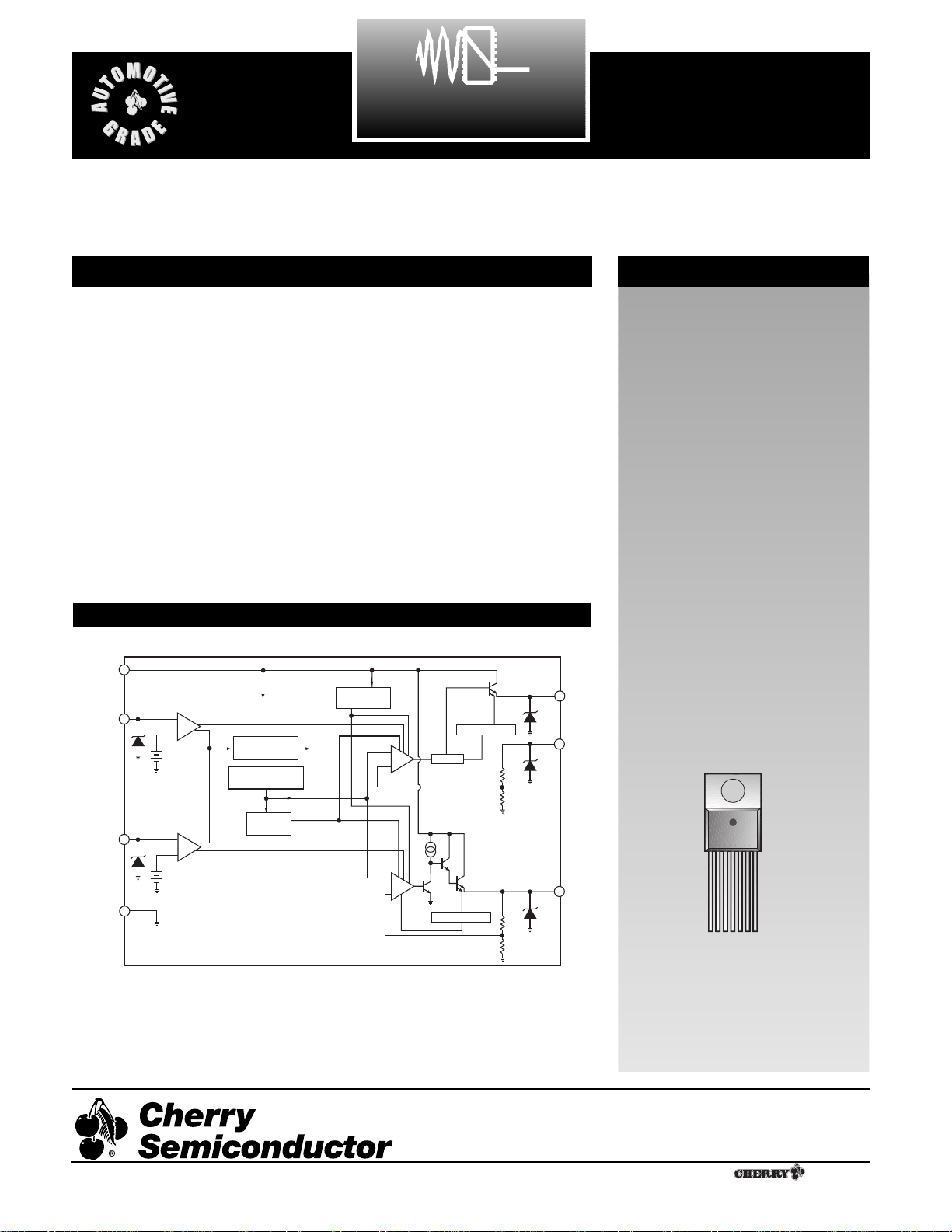
Block Diagram
The CS8371 is a 8V/5V dual output
linear regulator. The 8V ±5% output
sources 1A, while the 5V ±5% output sources 250mA. Each output is
controlled by its own ENABLE
lead. Setting the ENABLE input
high turns on the associated regulator output. Holding both ENABLE
inputs low puts the IC into sleep
mode where current consumption
is less than 10µA.
The regulator is protected against
overvoltage, short-circuit and ther-
mal runaway conditions. The
device can withstand 45V load
dump transients making suitable
for use in automotive environments. CherryÕs proprietary
NoCapª solution is the first technology which allows the output to
be stable without the use of an
external capacitor.
The CS8371 is available in a 7 lead
TO-220 package with copper tab.
The tab can be connected to a
heatsink if necessary.
1 ENABLE
1
2 ENABLE
2
3V
OUT2
4 Gnd
5 Sense
6V
CC
7V
OUT1
Rev. 6/9/99
Cherry Semiconductor Corporation
2000 South County Trail, East Greenwich, RI 02818
Tel: (401)885-3600 Fax: (401)885-5786
Email: info@cherry-semi.com
Web Site: www.cherry-semi.com
A Company
¨
NoCap is a trademark of Cherry Semiconductor Corporation, and is patented.
Pre-Regulator/
Bias Generator
Trimmed Bandgap
Voltage Reference
Thermal
Shutdown
ENABLE
ENABLE
V
Gnd
CC
1
2
-
+
1.2V
-
+
1.2V
Overvoltage
Shutdown
Current Limit
+
VIA
-
-
+
Current Limit
V
OUT1
Sense
V
OUT2
1
Page 2
2
CS8371
PARAMETER TEST CONDITIONS MIN TYP MAX UNIT
Electrical Characteristics: -40¡C ² TA² +85¡C, 10.5V ² VCC² 16.0V, ENABLE1= ENABLE2= 5.0V,
I
OUT1
= I
OUT2
= 5.0mA, unless otherwise stated.
■ Primary Output (V
OUT1
)
Output Voltage I
OUT1
= 1.0A 7.60 8.00 8.40 V
Line Regulation 10.5V ² VCC² 26V 50 mV
Load Regulation 5mA ² I
OUT1
² 1.0A 150 mV
Sleep Mode Quiescent VCC= 14V, ENABLE1= ENABLE2= 0V 0 0.2 10.0 µA
Current
Quiescent Current VCC= 14V, I
OUT1
= 1.0A, I
OUT2
= 250mA 30 mA
Dropout Voltage I
OUT1
= 250mA 1.2 V
Dropout Voltage I
OUT1
= 1.0A 1.5 V
Quiescent Bias Current I
OUT1
= 5mA, ENABLE2= 0V, VCC= 14V 10 mA
IQ= ICC- I
OUT1
Quiescent Bias Current I
OUT1
= 1.0A, ENABLE2= 0V, VCC= 14V 22 mA
IQ= ICC- I
OUT1
Ripple Rejection f = 120Hz, VCC= 14V with 1.0VPPAC, 90 dB
C
OUT
= 0µF
f = 10kHz, VCC= 14V with 1.0VPPAC, 74 dB
C
OUT
= 0µF
f = 20kHz, VCC= 14V with 1.0VPPAC, 68 dB
C
OUT
= 0µF
Current Limit VCC= 16V 1.1 2.5 A
Overshoot Voltage 5mA ² I
REG1
² 1.0A 6.0 V
Output Noise 10Hz-100kHz 300 µV
rms
■ Secondary Output (V
OUT2
)
Output Voltage I
OUT2
= 250mA 4.75 5.00 5.25 V
Line Regulation 7V ² VCC² 26V 40 mV
Load Regulation 5mA ² I
OUT2
² 250mA 100 mV
Dropout Voltage I
OUT2
= 5.0mA 2.2 V
Dropout Voltage I
OUT2
= 250mA 2.5 V
Quiescent Bias Current I
OUT2
= 5mA, ENABLE1= 0V, VCC= 14V 7 mA
IQ= ICC- I
OUT2
Quiescent Bias Current I
OUT2
= 250mA, ENABLE1= 0V, VCC= 14V 8 mA
IQ= ICC- I
OUT2
Ripple Rejection f = 120Hz, VCC= 14V with 1.0 VPPAC, 90 dB
C
OUT
= 0µF
f= 10kHz, VCC= 14V with 1.0VPPAC, 75 dB
C
OUT
= 0µF
f = 20kHz, VCC= 14V with 1.0VPPAC, 67 dB
C
OUT
= 0µF
Absolute Maximum Ratings
Power Dissipation.............................................................................................................................................Internally Limited
ENABLE Input Voltage Range .............................................................................................................................-0.6V to +10.0V
Load Current (8V Regulator)...........................................................................................................................Internally Limited
Load Current (5V Regulator)...........................................................................................................................Internally Limited
Transient Peak Voltage (31V load dump @ 14V V
CC
) ...........................................................................................................45V
Storage Temperature Range ................................................................................................................................-65¡C to +150¡C
Junction Temperature Range...............................................................................................................................-40¡C to +150¡C
Lead Temperature Soldering: Wave Solder (through hole styles only)..........................................10 sec. max, 260¡C peak
Page 3
3
Electrical Characteristics: -40¡C ² TA² +85¡C, 10.5V ² VCC² 16.0V, ENABLE1= ENABLE2= 5.0V,
I
OUT1
= I
OUT2
= 5.0mA, unless otherwise stated.
CS8371
Package Pin Description
PACKAGE PIN # PIN SYMBOL FUNCTION
7 Lead TO-220
1 ENABLE
1
ENABLE control for the 8V, 1A output
2 ENABLE
2
ENABLE control for the 5V, 250mA output
3V
OUT2
5V ±5%, 250mA regulated output
4 Gnd Ground
5 Sense Sense feedback for the primary 8V output
6V
CC
Supply voltage, usually from battery
7V
OUT1
8V ±5%, 1A regulated output
PARAMETER TEST CONDITIONS MIN TYP MAX UNIT
■ Secondary Output (V
OUT2
): continued
Current Limit VCC= 16V 270 600 mA
Overshoot Voltage 5mA ² I
REG2
² 250mA 4.3 V
Output Noise 10Hz-100kHz 170 µV
rms
■ ENABLE Function (ENABLE)
Input Current VCC= 14V, 0V ² ENABLE ² 5.5V -150 150 µA
Input Voltage Low 0 0.8 V
High 2.0 5.0 V
■ Protection Circuitry
ESD Threshold Human Body Model ±2.0 ±4.0 kV
Overvoltage Shutdown 24 30 V
Thermal Shutdown Guaranteed by Design 150 180 ¡C
Thermal Hysteresis 30 ¡C
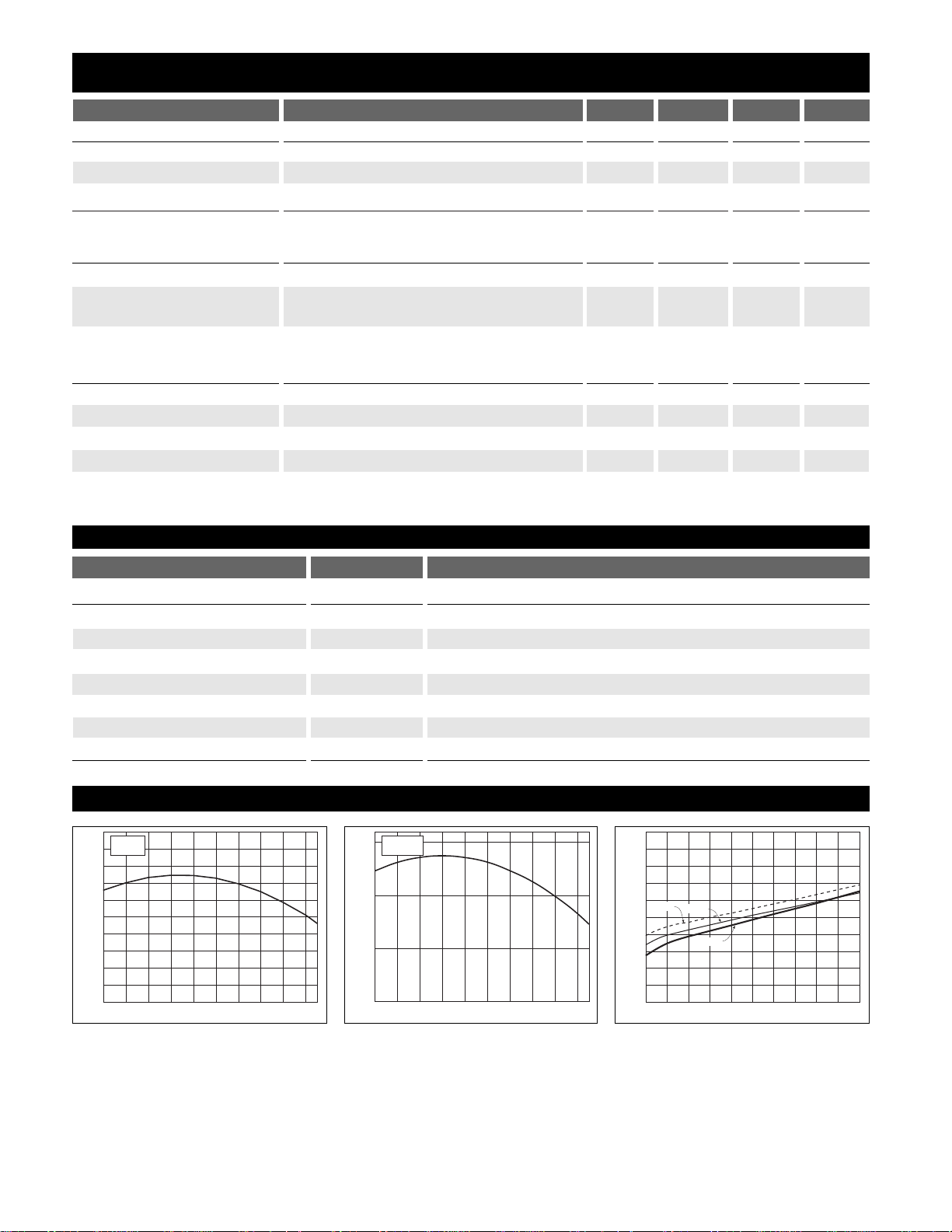
Typical Performance Characteristics
Regulator 1 Output Voltage Regulator 2 Output Voltage
Regulator 1 Dropout Voltage
8.05
VIN = 14V
8.04
= 1A
I
OUT
8.03
8.02
8.01
8.00
7.99
Output Voltage (V)
7.98
7.97
7.96
7.95
-40 -20 0 20 40 60 80 100 120 140
Ambient Temperature (°C)
5.00
4.95
Output Voltage (V)
4.90
4.85
-40 -20 0 20 40 60 80 100 120 140
VIN = 14V
= 250A
I
OUT
Ambient Temperature (°C)
2.0
1.8
1.6
1.4
1.2
-40°C
1.0
0.8
Dropout Voltage (V)
0.6
0.4
0.2
0
25°C
85°C
0 100 200 300 400 500 600 700 800 900
Output Current (mA)
1000
Page 4

4
CS8371
Typical Performance Characteristics: continued
Regulator 2 Dropout Voltage Regulator 1 Current Limit
Regulator 2 Current Limit
Quiescent Current Quiescent Current
Regulator 1 Quiescent Current
Regulator 2 Quiescent Current Regulator 1 Load Regulation
0
Regulator 2 Load Regulation
Regulator 1 Startup Regulator 2 Startup
Regulator 1 Line Transient Response
Dropout Voltage (V)
2.5
2.0
-40°C
1.5
25°C
85°C
1.0
0.5
0
0 50 100 150 200
Output Current (mA)
250
10
VIN = 14V
9
= 25°C
T
A
8
7
6
5
4
Reg 1 Output Voltage (V)
3
2
1
0
012
Reg 1 Output Current (A)
3
10
VIN = 14V
9
= 25°C
T
A
8
7
6
5
4
Reg 2 Output Voltage (V)
3
2
1
0
0 100 200
Reg 2 Output Current (mA)
300
400 500
9.0
Enable 1 = 5V
Enable 2 = 5V
8.5
V
= 14V
IN
8.0
1 = 1A
I
OUT
2 = 250mA
I
OUT
7.5
7.0
6.5
6.0
5.5
Quiescent Current (mA)
5.0
4.5
4.0
-40 -200 2040 6080
Ambient Temperature (°C)
1.0
Enable 1 = 0V
Enable 2 = 0V
0.9
= 14V
V
IN
0.8
0.7
0.6
0.5
0.4
0.3
Quiescent Current (mA)
0.2
0.1
0
-40 -200 2040 6080
Ambient Temperature (°C)
4.0
Enable 1 = 0V
Enable 2 = 5V
3.8
3.6
3.4
3.2
3.0
2.8
2.6
Quiescent Current (mA)
2.4
2.2
2.0
= 14V
V
IN
I
= 250mA
OUT
I
= 5mA
OUT
-40 -200 2040 6080
Ambient Temperature (°C)
8.020
VIN = 14V
8.015
8.010
8.005
8.000
7.995
Output Voltage (V)
7.990
7.985
7.980
25°C
0 100 200 300 400 500 600 700 800 900
Output Current (mA)
-40°C
85°C
6.0
Enable 1 = 5V
Enable 2 = 0V
V
= 14V
IN
5.5
5.0
4.5
I
= 5mA
OUT
4.0
Quiescent Current (mA)
3.5
3.0
-40 -200 2040 6080
Ambient Temperature (°C)
5.02
VIN = 14V
5.01
5.00
4.99
4.98
4.97
Output Voltage (V)
4.96
-40°C
4.95
4.94
100
0 50 100 150 200
Output Current (mA)
85°C
25°C
I
= 1A
OUT
250
C
8
T
7
I
OUT
6
5
4
3
2
1
0
Reg 1 Output Voltage (V)
5
4
3
2
1
Enable 1 (V)
0
01
= 0mF
OUT
= 25°C
A
= 5mA
23456789101112
Time (ms)
C
8
T
7
I
6
OUT
5
4
3
2
1
0
Reg 2 Output Voltage (V)
5
4
3
2
1
Enable 2 (V)
0
01
= 0mF
OUT
= 25°C
A
= 5mA
23456789101112
Time (ms)
C
= 0mF
OUT
T
= 25°C
A
2
1
0
-1
-2
Output Voltage Deviation (V)
16
14
12
10
Input Voltage (V)
0 100 200 300 400 500
Time (ns)
600
Page 5

5
Typical Performance Characteristics: continued
CS8371
C
Regulator 2 Line Transient Response Regulator 1 Load Transient Response
Regulator 2 Load Transient Response
Regulator 1 Ripple Rejection Regulator 2 Ripple Rejection
Regulator 1 Stability
Definition of Terms
Dropout Voltage: The input-output voltage differential at
which the circuit ceases to regulate against further
reduction in input voltage. Measured when the output
voltage has dropped 100mV from the nominal value
obtained at 14V input, dropout voltage is dependent
upon load current and junction temperature.
Current Limit: Peak current that can be delivered to the output.
Input Voltage: The DC voltage applied to the input terminals
with respect to ground.
Input Output Differential: The voltage difference between the
unregulated input voltage and the regulated output
voltage for which the regulator will operate.
Line Regulation: The change in output voltage for a change in
the input voltage. The measurement is made under
conditions of low dissipation or by using pulse techniques such that the average chip temperature is not
significantly affected.
Load Regulation: The change in output voltage for a change in
load current at constant chip temperature.
Long Term Stability: Output voltage stability under accelerat-
ed life-test conditions after 1000 hours with maximum
rated voltage and junction temperature.
Output Noise Voltage: The rms AC voltage at the output, with
constant load and no input ripple, measured over a
specified frequency range.
Quiescent Current: The part of the positive input current that
does not contribute to the positive load current. The
regulator ground lead current.
Ripple Rejection: The ratio of the peak-to-peak input ripple
voltage to the peak-to-peak output ripple voltage.
Temperature Stability of V
OUT
: The percentage change in out-
put voltage for a thermal variation from room temperature to either temperature extreme.
= 0mF
OUT
0.6
T
= 25°C
A
0.4
0.2
0
-0.2
-0.4
-0.6
Output Voltage Deviation (V)
16
14
12
10
Input Voltage (V)
0 100 200 300 400 500
Time (ns)
VIN = 14V
3
= 0mF
C
OUT
= 25°C
T
2
A
1
0
-1
-2
-3
Output Voltage Deviation (V)
1000
5
Load Current (mA)
600
0 5 10 15 20 25
Time (ms)
30
VIN = 14V
= 0mF
C
OUT
= 25°C
T
A
+500
0
-500
Output Voltage Deviation (mV)
250
5
0 5 10 15 20 25
Load Current (mA)
Time (ms)
30
TA = 25°C
= 14V
V
IN
= 0mF
C
OUT
100
80
60
Ripple Rejection (dB)
40
20
1 10 100 1k 10k 100k
Frequency (Hz)
1M
TA = 25°C
= 14V
V
IN
= 0mF
C
OUT
100
80
60
Ripple Rejection (dB)
40
20
1 10 100 1k 10k 100k
Frequency (Hz)
5
TA = 25°C
V
= 14V
IN
£ 1.6W
R
ESR
= 5ma to 1A
I
OUT
1
Unstable
Output Capacitor ESR (W)
1M
0.1
.01 0.1 1 10 100 1000
Region
Output Capacitor Size (mF)
Page 6

6
With separate control of each output channel, the CS8371
is ideal for applications where each load must be switched
independently. In an automotive radio, the 8V output
drives the displays and tape drive motors while the 5V
output supplies the Tuner IC and memory.
Stability Considerations/NoCapª
Normally a low dropout or quasi-low dropout regulator
(or any type requiring a slow lateral PNP in the control
loop) necessitates a large external compensation capacitor
at the output of the IC. The external capacitor is also used
to curtail overshoot, determine startup delay time and
load transient response.
Traditional LDO regulators typically have low unity gain
bandwidth, display overshoot and poor ripple rejection.
Compensation is also an issue because the high frequency
load capacitor value, ESR (Equivalent Series Resistance)
and board layout parasitics all can create oscillations if not
properly accounted for.
NoCapª is a Cherry Semiconductor exclusive output
stage which internally compensates the LDO regulator
over temperature, load and line variations without the
need for an expensive external capacitor. It incorporates
high gain (>80dB) and large unity gain bandwidth
(>100kHz) while maintaining many of the characteristics
of a single-pole amplifier (large phase margin and no
overshoot).
NoCapª is ideally suited for slow switching or steady
loads. If the load displays large transient current requirements, such as with high frequency microprocessors, an
output storage capacitor may be needed. Some large
capacitor and small capacitor ESR values at the output
may cause small signal oscillations at the output. This will
depend on the load conditions. With these types of loads,
a traditional output stage may be better suited for proper
operation.
Output 1 employs NoCapª. Refer to the plots in the
Typical Performance Characteristics section for appropriate output capacitor selections for stability if an external
capacitor is required by the switching characteristics of the
load. Output 2 has a Darlington NPN-type output structure and is inherently stable with any type of capacitive
load or no capacitor at all.
Applications Circuit
Application Notes
CS8371
C1*
0.1 mF
ENABLE
1
V
IN
V
OUT1
Gnd
V
OUT2
8V
5V
Control
DISPLAY
Tuner IC
ENABLE
2
CS8371
*C1is required if regulator is far from power source filter.
Page 7

7
Applications Notes: continued
CS8371
Calculating Power Dissipation
in a Dual Output Linear Regulator
The maximum power dissipation for a dual output regulator (Figure 1) is
P
D(max)
= {V
IN(max)
Ð V
OUT1(min)}IOUT1(max)
+
{V
IN(max)
Ð V
OUT2(min)}IOUT2(max)
+ V
IN(max)IQ
, (1)
where
V
IN(max)
is the maximum input voltage,
V
OUT1(min)
is the minimum output voltage from V
OUT
1
,
V
OUT2(min)
is the minimum output voltage from V
OUT
2
,
I
OUT1(max)
is the maximum output current, for the appli-
cation,
I
OUT2(max)
is the maximum output current, for the appli-
cation,
IQis the quiescent current the regulator consumes at
I
OUT(max)
.
Once the value of P
D(max)
is known, the maximum permis-
sible value of RQJAcan be calculated:
RQJA=
(2)
The value of RQJAcan then be compared with those in
the package section of the data sheet. Those packages
with RQJA's less than the calculated value in equation 2
will keep the die temperature below 150¡C.
In some cases, none of the packages will be sufficient to
dissipate the heat generated by the IC, and an external
heatsink will be required.
Heatsinks
A heatsink effectively increases the surface area of the
package to improve the flow of heat away from the IC and
into the surrounding air.
Each material in the heat flow path between the IC and the
outside environment will have a thermal resistance. Like
series electrical resistances, these resistances are summed
to determine the value of RQJA:
RQ
JA
= RQJC+ RQCS+ RQSA, (3)
where
RQJC= the junctionÐtoÐcase thermal resistance,
RQCS= the caseÐtoÐheatsink thermal resistance, and
RQSA= the heatsinkÐtoÐambient thermal resistance.
RQ
JC
appears in the package section of the data sheet. Like
RQJA, it too is a function of package type. RQCSand RQ
SA
are functions of the package type, heatsink and the interface between them. These values appear in heatsink data
sheets of heatsink manufacturers.
150¡C - T
A
P
D
Figure 1: Dual output regulator with key performance parameters
labeled.
I
V
IN
IN
Smart
Regulator
Control
Features
}
I
Q
I
OUT1
I
OUT2
V
V
OUT1
OUT2
Page 8

8
Rev. 6/9/99
© 1999 Cherry Semiconductor Corporation
CS8371
Part Number Description
CS8371ET7 7 Lead TO-220 Straight
CS8371ETVA7 7 Lead TO-220 Vertical
Thermal Data TO-220
RQ
JC
typ 2.4 ûC/W
RQ
JA
typ 50 ûC/W
Package Specification
PACKAGE THERMAL DATA
Ordering Information
Cherry Semiconductor Corporation reserves the right to
make changes to the specifications without notice. Please
contact Cherry Semiconductor Corporation for the latest
available information.
PACKAGE DIMENSIONS IN mm (INCHES)
7 Lead TO-220 (T) Straight
2.87 (.113)
2.62 (.103)
9.78 (.385)
10.54 (.415)
1.40 (.055)
1.14 (.045)
0.64 (.025)
0.38 (.015)
0.56 (.022)
0.36 (.014)
1.40 (.055)
1.14 (.045)
4.83 (.190)
4.06 (.160)
14.22 (.560)
13.72 (.540)
0.94 (.037)
0.58 (.023)
7.75 (.305)
7.49 (.295)
2.92 (.115)
2.29 (.090)
3.71 (.146)
3.96 (.156)
14.99 (.590)
14.22 (.560)
6.55 (.258)
5.94 (.234)
7 Lead TO-220 (TVA) Vertical
10.54 (.415)
9.78 (.385)
2.03 (.080)
7.52 (.296)
4.34
(.171)
1.40 (.055)
1.14 (.045)
14.99 (.590)
14.22 (.560)
11.86 (.467)
4.83 (.190)
4.06 (.160)
8.26
(.325)
7.62 (.300)
0.81
(.030)
1.27
(.050)
TYP
0.56 (.022)
0.36 (.014)
2.92 (.115)
2.29 (.090)
2.87 (.113)
2.62 (.103)
6.55 (.258)
5.94 (.234)
2.92
(.115)
3.96 (.156)
3.71 (.146)
 Loading...