

Datasheet CS8361YT7, CS8361YN16, CS8361YDWR20, CS8361YDWFR16, CS8361YDWF16 Datasheet (Cherry Semiconductor)
...Page 1
1
Features
■ 2 Regulated Outputs
Standby Output 5V
±2%; 100mA
Tracking Output 5V;
250mA
■ Low Dropout Voltage
(0.4V at rated current)
■ RESET Option
■ ENABLE Option
■ Low Quiescent Current
■ Protection Features
Independent Thermal
Shutdown
Short Circuit
60V Load Dump
Reverse Battery
Package Options
7L TO-220
CS8361
5V Dual Micropower Low Dropout
Regulator with ENABLE and RESET
CS8361
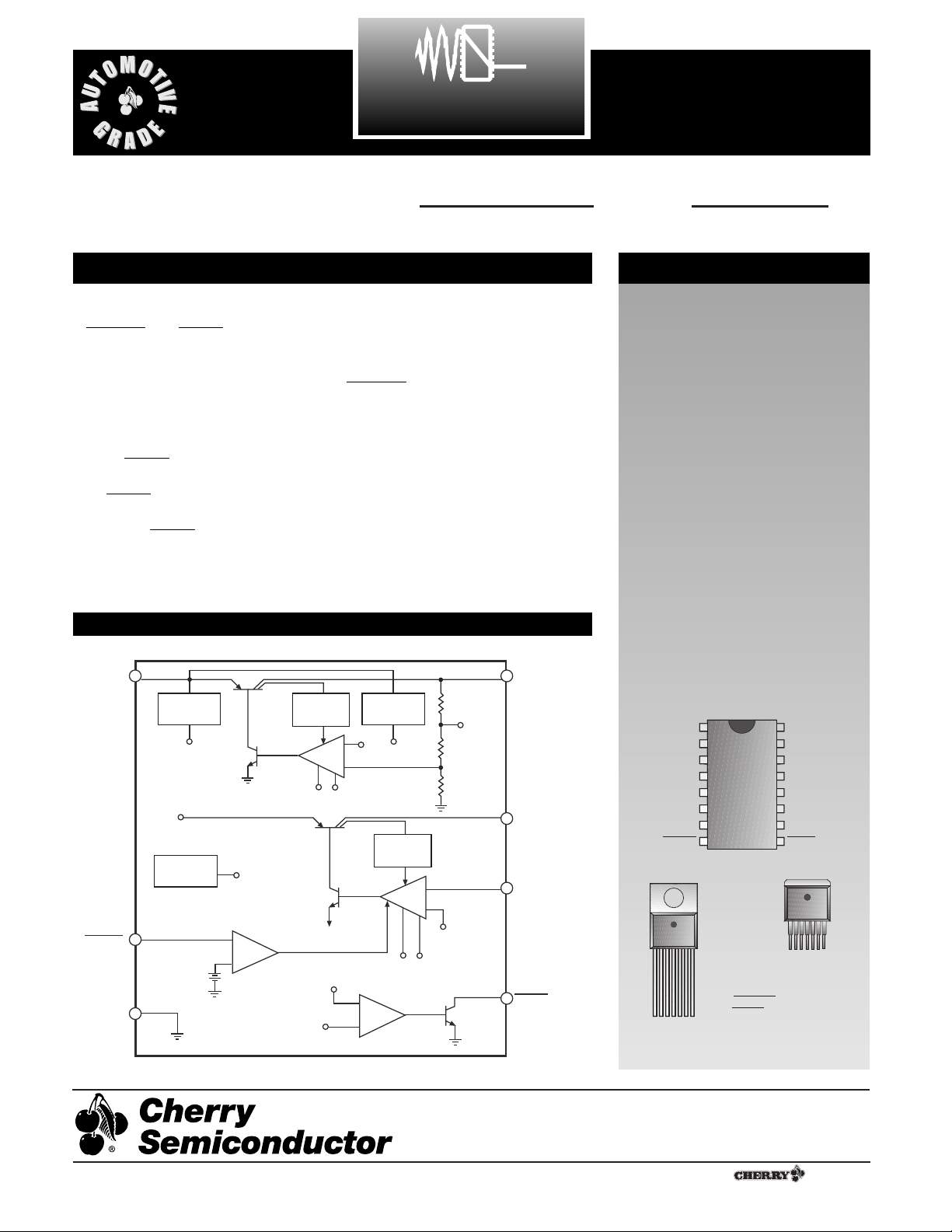
Block Diagram
Description
7L D2PAK
1
16 Lead PDIP & SOIC Wide
(internally fused leads)
NC
NC
NC
NC
NC
NC
V
IN
Gnd
Gnd
Gnd
Gnd
V
TRK
Adj
ENABLE
RESET
V
STBY
1. V
STBY
2. V
IN
3. V
TRK
4. Gnd
5. Adj
6. ENABLE
7. RESET
Also available in 20 Lead SOIC Wide.
Consult factory for 20 Lead PSOP .
* Consult factory for positive ENABLE option.
Rev. 5/4/99
The CS8361 is a precision micropower dual voltage regulator with
and .
The 5V standby output is accurate
within ±2% while supplying loads
of 100mA and has a typical
dropout voltage of 400mV.
Quiescent current is low, typically
140µA with a 300µA load. The
active output monitors the
5V standby output and holds
the line low during powerup and regulator dropout conditions. The circuit includes
hysteresis and is guaranteed to
operate correctly with 1V on the
standby output.
The second output tracks the 5V
standby output through an external
adjust lead, and can supply loads
of 250mA with a typical dropout
voltage of 400mV. The logic level
lead is used to control
this tracking regulator output.
Both outputs are protected against
overvoltage, short circuit, reverse
battery and overtemperature conditions. The robustness and low quiescent current of the CS8361 makes
it not only well suited for automotive microprocessor applications,
but for any battery powered microprocessor applications.
ENABLE
RESET
RESET
RESET
RESETENABLE
Cherry Semiconductor Corporation
2000 South County Trail, East Greenwich, RI 02818
Tel: (401)885-3600 Fax: (401)885-5786
Email: info@cherry-semi.com
Web Site: www.cherry-semi.com
A Company
®
V
IN
Overvoltage
Shutdown
OVSD
Current
Limit
Bandgap
BG
BG
+
–
RESET
V
STBY
5V,100mA,2%
1
V
IN
Thermal
Shutdown
ENABLE
Gnd
–
+
TSD
TSD
RESET
BG
OVSD
V
TRK
Current
Limit
–
+
V
STANDBY
OVSD
TSD
+
–
250mA
Adj
RESET
1
Page 2
2
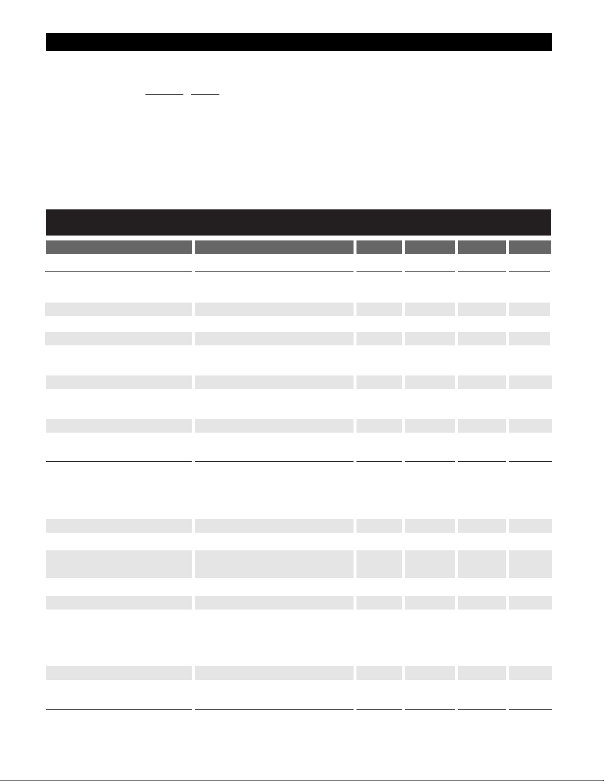
Electrical Characteristics: 6V ² V
IN
² 26V, I
OUT1
= I
OUT2
= 100µA, -40¡C ² TA ²+125¡C, -40¡C ²TJ² +150¡C,
unless otherwise specified.
PARAMETER TEST CONDITIONS MIN TYP MAX UNIT
CS8361
Absolute Maximum Ratings
Supply Voltage, V
IN
.....................................................................................................................................................-16V to 26V
Positive Transient Input Voltage, tr > 1ms.............................................................................................................................60V
Negative Transient Input Voltage, T < 100ms, 1% Duty Cycle..........................................................................................-50V
Input Voltage Range ( , ) ...............................................................................................................-0.3V to 10V
Junction Temperature...........................................................................................................................................-40¡C to +150¡C
Storage Temperature Range................................................................................................................................-55¡C to +150¡C
ESD Susceptibility (Human Body Model)..............................................................................................................................2kV
Lead Temperature Soldering
Wave Solder (through hole styles only) .....................................................................................10 sec. max, 260¡C peak
Reflow (SMD styles only) ......................................................................................60 sec. max above 183¡C, 230¡C peak
RESETENABLE
■ Tracking Output (V
TRK
)
V
STBY
Ð V
TRK
, 6V ² VIN² 26V -25 +25 mV
V
TRK
Tracking Error 100µA ² I
TRK
² 250mA (note 1)
Adjust Pin Current, I
Adj
Loop in Regulation 1.5 5 µA
Line Regulation 6V ² VIN² 26V (note 1) 5 50 mV
Load Regulation 100µA ² I
TRK
² 250mA (note 1) 5 50 mV
Dropout Voltage (VINÐ V
TRK
) I
TRK
= 100µA 100 150 mV
I
TRK
= 250mA 400 700 mV
Current Limit VIN= 12V, V
TRK
= 4.5 275 500 mA
Quiescent Current VIN= 12V, I
TRK
= 250mA 25 50 mA
No Load on V
STBY
Reverse Current V
TRK
= 5V, VIN= 0V 200 1500 µA
Ripple Rejection f = 120Hz, I
TRK
= 250mA 60 70 dB
7V ² VIN² 17V
■ Standby Output (V
STBY
)
Output Voltage, V
STBY
6V ² VIN² 26V 4.90 5.00 5.10 V
100µA ² I
STBY
² 100mA
Line Regulation 6V ² VIN² 26V 5 50 mV
Load Regulation 100µA ² I
STBY
² 100mA 5 50 mV
Dropout Voltage (VINÐ V
STBY
) I
STBY
= 100µA 100 150 mV
I
STBY
= 100mA 400 600 mV
Current Limit VIN= 12V, V
STBY
= 4.5V 125 200 mA
Short Circuit Current VIN= 12V, V
STBY
= 0V 10 100 mA
Quiescent Current V
IN
= 12V, I
STBY
= 100mA 10 20 mA
I
TRK
= 0mA
V
IN
= 12V, I
STBY
= 300µA 140 200 µA
I
TRK
= 0mA
Reverse Current V
STBY
= 5V, VIN= 0V 100 200 µA
Ripple Rejection f = 120Hz, I
STBY
= 100mA 60 70 dB
7V ² VIN² 17V
Note 1: V
TRK
connected to Adj lead. V
TRK
can be set to higher values by using an external resistor divider.
Page 3

CS8361
3
Package Lead Description
PACKAGE LEAD # LEAD SYMBOL FUNCTION
Electrical Characteristics: 6V ² V
IN
² 26V, I
OUT1
= I
OUT2
= 100µA, -40¡C ² TA ²+125¡C, -40¡C ²TJ² +150¡C,
unless otherwise specified.
PARAMETER TEST CONDITIONS MIN TYP MAX UNIT
■ Functions
Input Threshold 0.8 1.2 2.0 V
Input Bias Current V
ENABLE
= 0V to 10V -10 0 10 µA
Threshold High (VRH)V
STBY
Increasing 4.59 4.87 V
STBY
-0.02 V
Hysteresis 60 120 180 mV
Threshold Low (VRL)V
STBY
Decreasing 4.53 4.75 V
STBY
-0.08 V
Leakage 25 µA
Output Voltage
Low (V
RLO
); R
RST
= 10k½ 1V ² VS
TBY²VRL
0.1 0.4 V
Low (V
RPEAK
)V
STBY
, Power Up, Power Down 0.6 1.0 V
■ Protection Circuitry (Both Outputs)
Independent Thermal Shutdown V
STBY
150 180 ¡C
V
TRK
150 165 ¡C
Overvoltage Shutdown 30 34 38 V
RESET
RESET
RESET
RESET
ENABLE
ENABLE
ENABLERESET
16L PDIP & SO 20L SO Wide
7L 7L Wide (Internally (Internally
TO-220 D2PAK Fused Leads) Fused Leads)
1 1 16 20 V
STBY
Standby output voltage delivering 100mA.
22 1 1 V
IN
Input voltage.
33 3 2 V
TRK
Tracking output voltage controlled by
delivering 250mA.
4 4 4,5,12,13 4,5,6,7 Gnd Reference ground connection.
14,15,16,17
5 5 6 8 Adj Resistor divider from V
TRK
to Adj. Sets the
output voltage on V
TRK
. If tied to V
TRK
, V
TRK
will track V
STBY
.
66 8
10
Provides on/off control of the tracking output,
active LOW.
7 7 9 11 CMOS compatible output lead that goes low
whenever V
STBY
falls out of regulation.
2,7,10, 3,9,12,13, NC No Connection.
11,14,15 18,19
RESET
ENABLE
ENABLE
Page 4

4
CS8361
Circuit Description
Application Notes
The function switches the output transistor for
V
TRK
on and off. When the lead voltage exceeds
1.4V(typ), V
TRK
turns off. This input has several hundred
millivolts of hysteresis to prevent spurious output activity
during power-up or power-down.
The is an open collector NPN transistor, controlled by a low voltage detection circuit sensing the V
STBY
(5V) output voltage. This circuit guarantees the
output stays below 1V (0.1V typ) when V
STBY
is as low as
1V to ensure reliable operation of microprocessor-based
systems.
This output uses the same type of output device as V
STBY
,
but is rated for 250mA. The output is configured as a
tracking regulator of the standby output. By using the
standby output as a voltage reference, giving the user an
external programming lead (Adj lead), output voltages
from 5V to 20V are easily realized. The programming is
done with a simple resistor divider (Figure 2), and following the formula:
V
TRK
= V
STBY
´ (1 + R1/R2) + I
Adj
´ R1
If another 5V output is needed, simply connect the Adj
lead to the V
TRK
output lead.
V
TRK
Output Voltage
RESET
RESET
RESET Function
ENABLE
ENABLE
ENABLE Function
Output capacitors for the CS8361 are required for stability.
Without them, the regulator outputs will oscillate. Actual
size and type may vary depending upon the application
load and temperature range. Capacitor effective series
resistance (ESR) is also a factor in the IC stability. Worstcase is determined at the minimum ambient temperature
and maximum load expected.
Output capacitors can be increased in size to any desired
value above the minimum. One possible purpose of this
would be to maintain the output voltages during brief
conditions of negative input transients that might be characteristic of a particular system.
Capacitors must also be rated at all ambient temperatures
expected in the system. To maintain regulator stability
down to -40ûC, capacitors rated at that temperature must
be used.
More information on capacitor selection for Smart
Regulatorsª is available in the Smart Regulator application note, ÒCompensation for Linear Regulators.Ó
The maximum power dissipation for a dual output regulator (Figure 1) is:
PD(max) = {VIN(max)ÐV
OUT1
(min)}I
OUT1
(max)+
{V
IN
(max)ÐV
OUT2
(min)}I
OUT2
(max)+VIN(max)IQ (1)
Where
VIN(max) is the maximum input voltage,
V
OUT1
(min) is the minimum output voltage from V
OUT1
,
V
OUT2
(min) is the minimum output voltage from V
OUT2
,
I
OUT1
(max) is the maximum output current, for the
application
I
OUT2
(max) is the maximum output current, for the
application
IQis the quiescent current the regulator consumes at
I
OUT
(max).
Once the value of PD(max) is known, the maximum permissible value of R
QJA
can be calculated:
R
QJA
= (2)
The value of R
QJA
can then be compared with those in
the package section of the data sheet. Those packages
with R
QJA
's less than the calculated value in equation 2
will keep the die temperature below 150¡C.
In some cases, none of the packages will be sufficient to
dissipate the heat generated by the IC, and an external
heat sink will be required.
Figure 1: Dual output regulator with key performance parameters
labeled.
150¡C - T
A
P
D
Calculating Power Dissipation
in a Dual Output Linear Regulator
External Capacitors
I
V
IN
IN
Smart
Regulator
Control
Features
}
I
Q
I
OUT1
I
OUT2
V
V
OUT1
OUT2
Page 5

5
CS8361
Test & Application Circuits
A heat sink effectively increases the surface area of the
package to improve the flow of heat away from the IC and
into the surrounding air.
Each material in the heat flow path between the IC and the
outside environment will have a thermal resistance. Like
series electrical resistances, these resistances are summed
to determine the value of R
QJA
:
R
QJA
= R
QJC
+ R
QCS
+ R
QSA
(3)
where:
R
QJC
= the junctionÐtoÐcase thermal resistance,
R
QCS
= the caseÐtoÐheat sink thermal resistance, and
R
QSA
= the heat sinkÐtoÐambient thermal resistance.
R
QJC
appears in the package section of the data sheet. Like
R
QJA
, it too is a function of package type. R
QCS
and R
QSA
are functions of the package type, heat sink and the interface between them. These values appear in heat sink data
sheets of heat sink manufacturers.
Heat Sinks
Application Notes: continued
Figure 2: 5V, 8V Regulator
Figure 3: Dual 5V Regulator
B+
0.1µF
C1*
V
IN
V
STBY
CS8361
RESET
ENABLE
Adj
Gnd
V
TRK
R3
R1
C3**
R2
10µF
ESR<8Ω
5V, 100mA
C2**
SW 8V,
250mA
10µF
ESR<8Ω
V
DD
RESET
I/O
Gnd
MCU
* C1 is required if regulator is located far from power supply filter.
** C2 and C3 are required for stability.
B+
0.1µF
C1*
For V
V
IN
Gnd
V
TRK
CS8361
~ V
TRK
(1 + R1/R2)
STBY
~ 8V, R1/R2 ~ 0.6
V
STBY
RESET
ENABLE
Adj
V
TRK
R1
C3**
5V, 100mA
C2**
10µF
ESR<8Ω
10µF
ESR<8Ω
SW 5V,
250mA
V
DD
RESET
I/O
Gnd
MCU
* C1 is required if regulator is located far from power supply filter.
** C2 and C3 are required for stability.
Page 6

D
Lead Count Metric English
Max Min Max Min
16L PDIP 19.69 18.67 .775 .735
16L SO Wide* 10.50 10.10 .413 .398
20L SO Wide* 13.00 12.60 .512 .496
Part Number Description
CS8361YDPS7 7L D2PAK short-leaded
CS8361YDPSR7 7L D2PAK short-leaded, (tape & reel)
CS8361YT7 7L TO-220 (Straight)
CS8361YDWF16 16L SO Wide*
CS8361YDWFR16 16L SO Wide*, (tape & reel)
CS8361YN16 16L PDIP
CS8361YDW20 20L SO Wide*
CS8361YDWR20 20L SO Wide*, (tape & reel)
6
Ordering Information
Rev. 5/4/99 © 1999 Cherry Semiconductor Corporation
CS8361
Cherry Semiconductor Corporation reserves the right to
make changes to the specifications without notice. Please
contact Cherry Semiconductor Corporation for the latest
available information.
Package Specification
PACKAGE DIMENSIONS IN mm(INCHES)
PACKAGE THERMAL DATA
Thermal Data typ R
QJA
R
QJC
ûC/W
7L D2PAK 10-50
**
3.5
7L TO-220 50 3.5
16L PDIP 80 42
16L SO Wide* 75 18
20L SO Wide* 55 9
** Depending on thermal properties of substrate. R
Q
JA
= R
Q
JC
+ R
Q
CA
Plastic DIP (N); 300 mil wide
0.39 (.015)
MIN.
2.54 (.100) BSC
1.77 (.070)
1.14 (.045)
D
Some 8 and 16 lead
packages may have
1/2 lead at the end
of the package.
All specs are the same.
.203 (.008)
.356 (.014)
REF: JEDEC MS-001
3.68 (.145)
2.92 (.115)
8.26 (.325)
7.62 (.300)
7.11 (.280)
6.10 (.240)
.356 (.014)
.558 (.022)
Surface Mount Wide Body (DW); 300 mil wide
1.27 (.050) BSC
7.60 (.299)
7.40 (.291)
10.65 (.419)
10.00 (.394)
D
0.32 (.013)
0.23 (.009)
1.27 (.050)
0.40 (.016)
REF: JEDEC MS-013
2.49 (.098)
2.24 (.088)
0.51 (.020)
0.33 (.013)
2.65 (.104)
2.35 (.093)
0.30 (.012)
0.10 (.004)
* Internally Fused Leads
7 Lead D2PAK (DPS)* Short-Leaded
1.98 (.078)
1.47 (.058)
14.71 (.579)
13.69 (.539)
4.57 (.180)
4.31 (.170)
1.40 (.055)
1.14 (.045)
2.79 (.110)
2.54 (.100)
TERMINAL 8
7.75 (.305)
REF
6.50 (.256) REF
10.31 (.406)
10.05 (.396)
1.27 (.050)
REF
1.68 (.066)
1.40 (.055)
.254 (.010)
REF
0.91 (.036)
0.66 (.026)
8.53 (.336)
8.28 (.326)
0.10 (.004)
0.00 (.000)
*CHERRY SEMICONDUCTOR SHORT-LEADED FOOTPRINT
7 Lead TO-220 (T) Straight
2.87 (.113)
2.62 (.103)
9.78 (.385)
10.54 (.415)
1.40 (.055)
1.14 (.045)
0.64 (.025)
0.38 (.015)
0.56 (.022)
0.36 (.014)
1.40 (.055)
1.14 (.045)
4.83 (.190)
4.06 (.160)
14.22 (.560)
13.72 (.540)
0.94 (.037)
0.58 (.023)
7.75 (.305)
7.49 (.295)
2.92 (.115)
2.29 (.090)
3.71 (.146)
3.96 (.156)
14.99 (.590)
14.22 (.560)
6.55 (.258)
5.94 (.234)
 Loading...