

Page 1
1
Features
■ µP Compatible Inputs
■ Adjustable Current Limit
Thresholds
■ External Sense Resistor
■ Flag Signal to Indicate
Output Status
Package Options
8L PDIP & SO Narrow
CS8312
IGBT Ignition Predriver
with Dynamic Current Regulation
Description
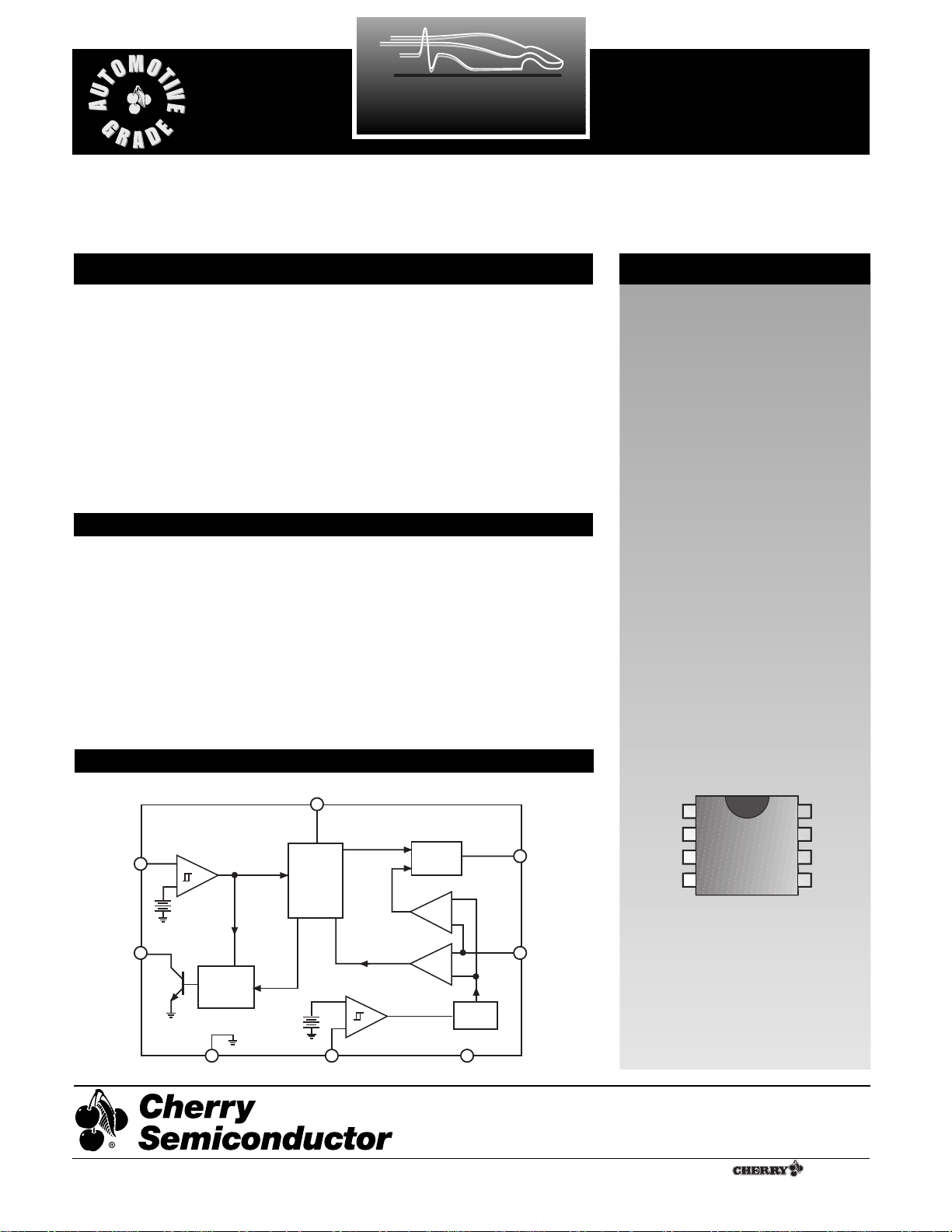
Block Diagram
Absolute Maximum Ratings
The CS8312 is a bipolar microprocessor interface IC designed to
drive an IGBT (or logic level
MOSFETs) powering large inductive loads in harsh operating environments. The ICÕs dynamic current limit function lets the microprocessor adjust the current limit
threshold to the real time needs of
the system.
CLI, the current limit input, sets the
current limit for the IGBT high or
low as directed by the system
microprocessor. CLI also raises and
lowers the threshold on the diagnostic FLAG output signal. The
FLAG output signals the microprocessor when the current level
approaches current limit on the
IGBT. The CTRL input enables the
FLAG function.
CS8312
Supply Voltage.................................................................................-0.3V to +12V
Digital Input Currents....................................................................................2mA
Internal Power Dissipation (TA= 25¡C) .................................................700mW
Junction Temperature Range.....................................................-40¡C to +150¡C
Storage Temperature Range ......................................................-55¡C to +165¡C
Lead Temperature Soldering
Wave Solder(through hole styles only).............10 sec. max, 260¡C peak
Reflow (SMD styles only).............60 sec. max above 183¡C, 230¡C peak
Electrostatic Discharge (Human Body Model) ............................................2kV
A Company
¨
Rev. 4/7/97
Cherry Semiconductor Corporation
2000 South County Trail, East Greenwich, RI 02818
Tel: (401)885-3600 Fax: (401)885-5786
Email: info@cherry-semi.com
Web Site: www.cherry-semi.com
CTRL
FLAG
V
Control
Logic
V
T
CC
Gate
Driver
SENSEÐCLIGnd
1
FLAG
SENSE+
OUT
SENSE+
V
REF
SENSEÐ
Gnd
V
CC
CTRL
CLI
OUT
V
T
Latch
Page 2
2
Electrical Characteristics 7V ² VCC² 10V; -40¡C ² TA² +125¡C; unless otherwise specified
PARAMETER TEST CONDITIONS MIN TYP MAX UNIT
CS8312
■ General
Power Supply 7 10 V
including Ripple Voltage
Supply Ripple Frequency 10 60 kHz
Differential Ground Voltage DC SENSE- to Gnd -0.1 1.0 V
AC SENSE- to Gnd -0.2 0.6 V
Differential Ground Frequency 10 60 kHz
Quiescent Current, I
Q
Turn On V
CTRL
=5.5V 15 mA
Turn Off V
CTRL
=-0.3V 5 mA
Supply Voltage Rejection V
CTRL
=5.5V 30 dB
Differential Ground V
CTRL
=5.5V 30 dB
Rejection Ratio
Differential Ground Current V
CTRL
= -0.3V 3 mA
Ratio (V
SENSE--VGnd
)DC=1V
(V
SENSE--VGnd
)AC=0.6V
Unity Gain Bandwidth V
CTRL
=5.5V 400 kHz
Clamp Voltage V
CTRL
=5.5V; I
OUT
=1mA 5.5 V
Output Off Voltage V
CTRL
=-0.3V; I
OUT
=10µA 0.5 V
V
CTRL
=-0.3V; I
OUT
=200µA 1.2 V
Turn On Delay CTRL increasing 30 us
Turn Off Delay CTRL decreasing 30 us
■ Control Function
Input Voltage Range I
CTRL
=2mA -0.3 5.5 V
Input Threshold
Turn On CTRL increasing 3.5 V
Turn Off CTRL decreasing 1.5 V
Hysteresis 0.4 2.0 V
Voltage I
CTRL
=10µA MAX 1.1 V
Input Capacitance 50 pF
■ Current Limit Increase Function
Input Voltage Range I
CTRL
=2mA -0.3 5.5 V
Input Threshold
Turn On CLI increasing 3.5 V
Turn Off CLI decreasing 1.5 V
Hysteresis 0.4 2.0 V
Voltage I
CLI
=10µA max 1.1 V
Input Capacitance 50 pF
■ Output Stage
I
OUT
5mA
■ Flag Function
Output Low V
CTRL
=5.5V; I
FLAG
=1.5mA 0.9 V
Leakage Current V
CTRL
=-0.3V 10 µA
Output Capacitance 50 pF
Turn On (V
SENSE+
Ð V
SENSE-
)V
CTRL
=5.5V; V
CLI
=-0.3V 210 225 240 mV
V
CTRL
=5.5V; V
CLI
=5.5V 300 350 mV
Page 3

3
Electrical Characteristics continued
PARAMETER TEST CONDITIONS MIN TYP MAX UNIT
CS8312
Package Pin Description
PACKAGE PIN # PIN SYMBOL FUNCTION
8L PDIP & SO
1 FLAG Indicates whether current through the IGBT has reached a pre-
set level.
2 SENSE+ Positive input to current comparator.
3 SENSEÐ Ground (SENSE-) for current sense resistor.
4 Gnd Ground connection.
5 OUT Output voltage to IGBT (MOSFET) gate.
6 CLI Current limit input increase.
7 CTRL Control input.
8V
CC
Supply voltage.
The flag indicates when the voltage across the two sense
pins is approaching a current limit level that has been
determined by the value of the external sense resistor
(R
SENSE
) and the state of the CTRL and CLI pins. If the
voltage across the sense pins (SENSE+, SENSE-) is less
than the flag turn-on voltage, then the FLAG is off. When
the voltage between the sense pins equals the FLAG turn
on voltage, the FLAG will latch on until the CTRL pin
goes low. FLAG is disabled whenever CTRL is low.
Changing the CLI pin from low to high will increase
nominal FLAG turn on voltage by approximately 45%.
Table 1 FLAG Timing Sequence
The CS8312 output (OUT) saturates and supplies voltage
to the IGBT (or MOSFET) gate once the CTRL switches
from low to high. As current through the IGBT (MOSFET)
increases and the voltage across the sense resistor passes
the flag turn on voltage, the FLAG will turn on. If the current through the sense resistor continues to rise and the
sense resistor voltage reaches the regulation sense voltage, then the gate voltage will fall to a level that regulates
the driver and maintains the regulation sense voltage at
the sense resistor.
Changing the CLI pin from a logic low to a logic high
increases the FLAG turn on voltage by approximately
45% and the regulation sense voltage by approximately
39% respectively.
Current Limit Function
Output Stage
State CONTROL SENSE+ FLAG
0 Low X OFF
1 High Below Threshold OFF
2 High Above Threshold ON
3 High X ON
0 Low X OFF
Flag Function (see Application Diagram)
Circuit Description
■ Flag Function: continued
Turn Off Delay CTRL decreasing 10 us
Turn On Delay 10 us
Disable Time 100 450 us
■ Sense Function
Input Voltage Range -0.3 2.5 V
Sense Regulation Voltage V
CTRL
=5.5V; V
CLI
=-0.3V 270 295 320 mV
V
CTRL
=5.5V; V
CLI
=5.5V 380 410 440 mV
Input Leakage Current V
CTRL
=5.5V 5 µA
Propagation Delay V
CTRL
=5.5V 20 us
Page 4

4
Application and Test Diagram
CS8312
Microprocessor
V
CC
V
BA
T
LOAD
0.1mF
V
CC
V
CC
OUT
R
CS8312
FLAG
CTRL
CLI
SENSE+
R
SENSE
SENSEÐ
Gnd
Page 5

Part Number Description
CS8312YN8 8L PDIP
CS8312YD8 8L SO Narrow
CS8312YDR8 8L SO Narrow (tape & reel)
5
CS8312
Thermal Data 8L SO 8L PDIP
R
QJC
typ 45 52 ûC/W
R
QJA
typ 165 100 ûC/W
Package Specification
PACKAGE DIMENSIONS IN mm (INCHES)
Ordering Information
PACKAGE THERMAL DATA
Rev. 4/7/97
D
Lead Count Metric English
Max Min Max Min
8 Lead SO Narrow 5.00 4.80 .197 .189
8 Lead PDIP 10.16 9.02 .400 .355
© 1999 Cherry Semiconductor Corporation
Cherry Semiconductor Corporation reserves the
right to make changes to the specifications without
notice. Please contact Cherry Semiconductor
Corporation for the latest available information.
Surface Mount Narrow Body (D); 150 mil wide
Plastic DIP (N); 300 mil wide
0.39 (.015)
MIN.
2.54 (.100) BSC
1.77 (.070)
1.14 (.045)
D
Some 8 and 16 lead
packages may have
1/2 lead at the end
of the package.
All specs are the same.
.203 (.008)
.356 (.014)
REF: JEDEC MS-001
3.68 (.145)
2.92 (.115)
8.26 (.325)
7.62 (.300)
7.11 (.280)
6.10 (.240)
.356 (.014)
.558 (.022)
1.27 (.050) BSC
0.51 (.020)
0.33 (.013)
6.20 (.244)
5.80 (.228)
4.00 (.157)
3.80 (.150)
1.57 (.062)
1.37 (.054)
D
0.25 (0.10)
0.10 (.004)
1.75 (.069) MAX
1.27 (.050)
0.40 (.016)
REF: JEDEC MS-012
0.25 (.010)
0.19 (.008)
 Loading...