

Page 1
查询CS8183YDWF20供应商
CS8183
Dual Micropower 200 mA
Low Dropout Tracking
Regulator/Line Driver
The CS8183 is a dual low dropout tracking regulator designed to
provide adjustable buffered output voltages that closely track
(±10 mV) the reference inputs. The outputs deliver up to 200 mA
while being able to be configured higher, lower or equal to the
reference voltages.
The outputs have been designed to operate over a wide range (2.8 V
to 45 V) while still maintaining excellent DC characteristics. The
CS8183 is protected from reverse battery, short circuit and thermal
runaway conditions. The device also can withstand 45 V load dump
transients and −50 V reverse polarity input voltage transients. This
makes it suitable for use in automotive environments.
The V
provide the input voltage as a reference for the output and they also
can be pulled low to place the device in sleep mode where it nominally
draws less than 30 µA from the supply.
The two trackers can be combined in parallel doubling the capability
to 400 mA for a single application.
Features
• Two Regulated Outputs 200 mA, ±10 mV Track Worst Case
• Low Dropout (0.35 V typ. @ 200 mA)
• Low Quiescent Current
• Independent Thermal Shutdown
• Short Circuit Protection
• Wide Operating Range
• Internally Fused Leads in the SO−20L Package
/ENABLE leads serve two purposes. They are used to
REF
http://onsemi.com
20
SO−20L
DWF
SUFFIX
CASE 751D
PIN CONNECTIONS AND
MARKING DIAGRAM
1
V
IN1
V
OUT1
GND
GND
V
REF
ADJ1
/ENABLE1
A = Assembly Location
WL, L = Wafer Lot
YY, Y = Year
WW, W = Work Week
AWLYYWW
1
CS8183
20
V
OUT2
V
IN2
NCNC
NCNC
GND
GND
NCNC
NCNC
V
REF
V
ADJ2
/ENABLE2V
Semiconductor Components Industries, LLC, 2004
March, 2004 − Rev. 15
ORDERING INFORMATION
Device Package Shipping
CS8183YDWF20
CS8183YDWFR20
1 Publication Order Number:
SO−20L
SO−20L
37 Units/Rail
1000 Tape & Reel
CS8183/D
Page 2
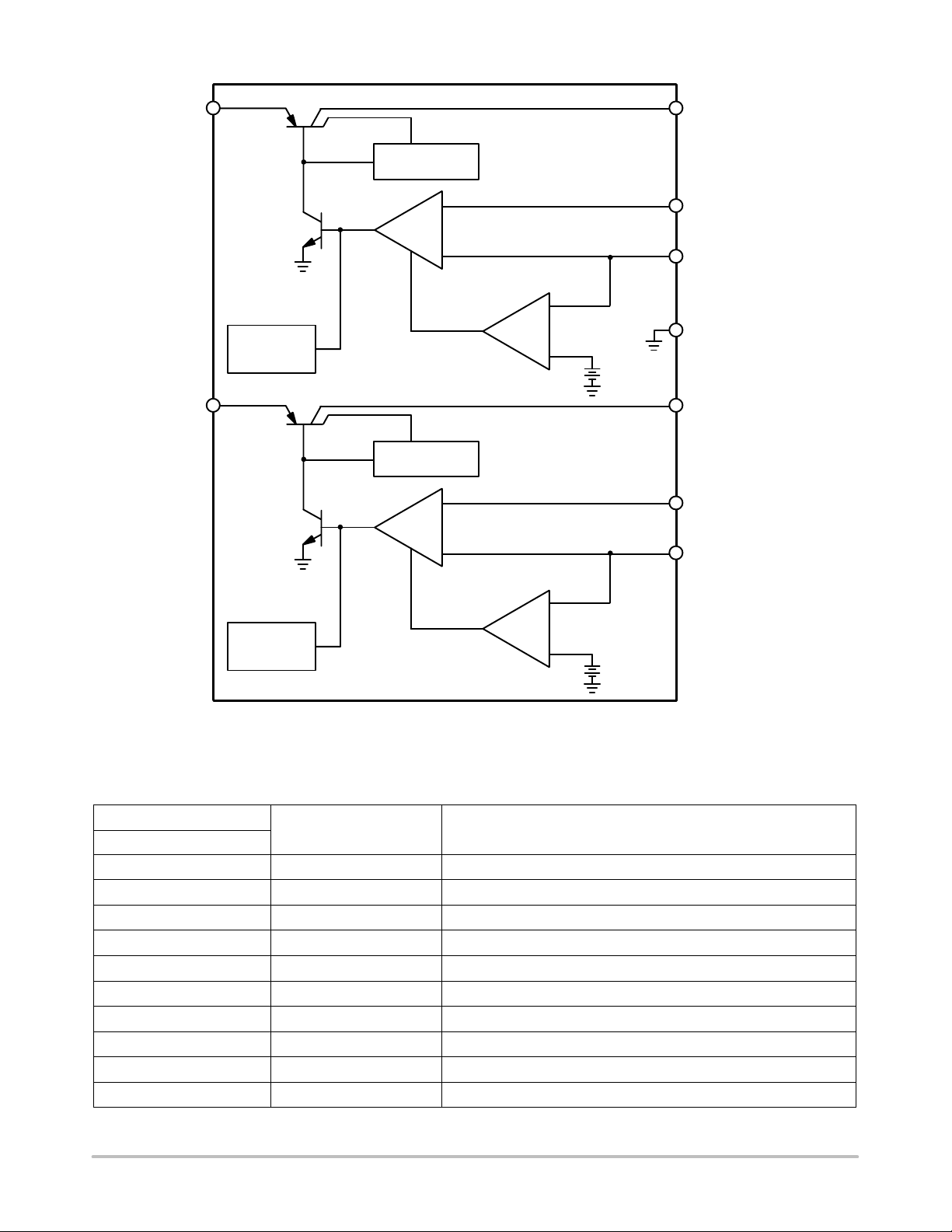
CS8183
V
IN1
V
OUT1
Current Limit &
VSAT Sense
−
ENABLE
+
Adj1
V
REF
/ENABLE1
+
Independent
Thermal
Shutdown
V
IN2
−
2.0 V
GND
V
OUT2
Current Limit &
VSAT Sense
−
ENABLE
+
Adj2
V
REF
/ENABLE2
Independent
Thermal
Shutdown
Figure 1. Block Diagram
PACKAGE PIN DESCRIPTION
Package Lead Number
SO−20L
1 V
2 V
3, 4, 7, 8, 13, 14, 17, 18 NC No connection.
5, 6, 15, 16 GND Ground (4 leads fused)
9 V
10 V
11 V
12 V
19 V
20 V
Lead Symbol Function
IN1
OUT1
ADJ1
/ENABLE1 Reference voltage and ENABLE input for V
REF
ADJ2
/ENABLE2 Reference voltage and ENABLE input for V
REF
IN2
OUT2
Input voltage for V
Regulated output voltage 1.
Adjust lead for V
Adjust lead for V
Input voltage for V
Regulated output voltage 2.
+
−
OUT1
OUT1
OUT2
OUT2
2.0 V
.
.
.
OUT1
.
.
OUT2
.
http://onsemi.com
2
Page 3
CS8183
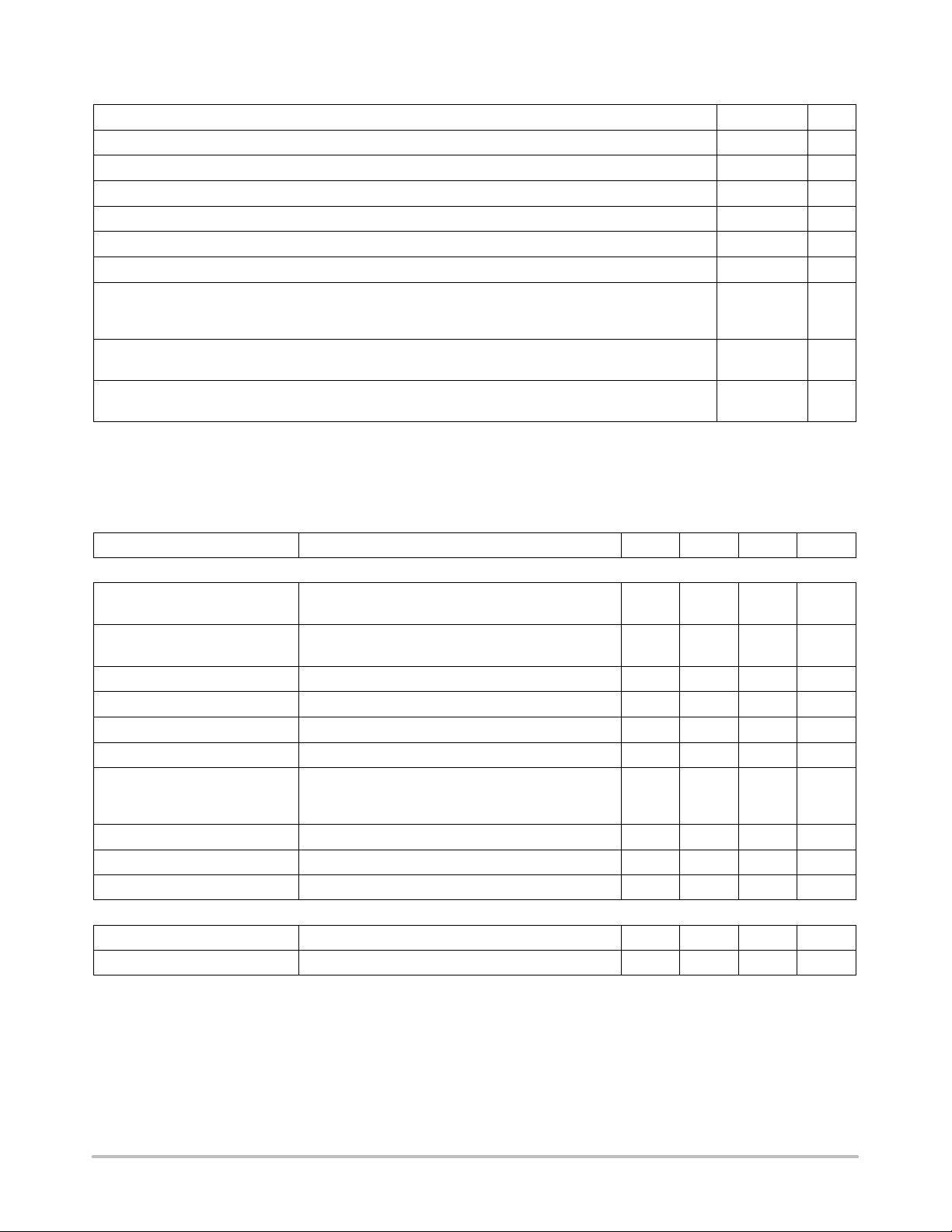
MAXIMUM RATINGS*
Rating Value Unit
Storage Temperature −65 to 150 °C
Supply Voltage Range (continuous) 15 to 45 V
Supply Voltage Range (normal, continuous) 3.4 to 45 V
Peak Transient Voltage (VIN = 14 V, Load Dump Transient = 31 V) 45 V
Voltage Range (Adj, V
Maximum Junction Temperature 150 °C
Package Thermal Resistance:
Junction−to−Case, R
Junction−to−Ambient, R
ESD Capability (Human Body Model)
(Machine Model)
Lead Temperature Soldering: Reflow: (SMD styles only) (Note 1) 240 peak
1. 60 second maximum above 183°C.
2. −5°C/+0°C allowable conditions.
*The maximum package power dissipation must be observed.
/ENABLE, V
REF
θ
JC
θ
JA
) −10 to 45 V
OUT
18
73
2.0
200
(Note 2)
°C/W
°C/W
kV
V
°C
ELECTRICAL CHARACTERISTICS (V
0.1 Ω < C
OUT − ESR
< 1.0 Ω @ 10 kHz; unless otherwise stated.)
Parameter
= 14 V; V
IN
/ENABLE > 2.75 V; −40°C ≤ TJ ≤ +125°C; C
REF
OUT
≥ 10 µF;
Test Conditions Min Typ Max Unit
Regular Output 1, 2
V
− V
REF
OUT
V
Tracking Error
OUT
Dropout Voltage (VIN − V
OUT
) I
4.5 V ≤ VIN ≤ 26 V, 100 µA ≤ I
= 100 µA
OUT
I
= 200 mA
OUT
≤ 200 mA, Note 3 −10 − 10 mV
OUT
−
−
100
350
150
600
Line Regulation 4.5 V ≤ VIN ≤ 26 V, Note 3 − − 10 mV
Load Regulation 100 µA ≤ I
≤ 200 mA, Note 3 − − 10 mV
OUT
Adj Lead Current Loop in Regulation − 0.2 1.0 µA
Current Limit VIN = 14 V, V
Quiescent Current (IIN − I
Reverse Current V
) VIN = 12 V, I
OUT
V
IN
V
IN
OUT
= 12 V, I
= 12 V, V
= 5.0 V, VIN = 0 V − 0.2 1.5 mA
= 5.0 V, V
REF
= 200 mA
OUT
= 100 µA
OUT
/ENABLE = 0 V
REF
= 90% of V
OUT
, Note 3 225 − 700 mA
REF
−
−
−
15
75
30
25
150
55
Ripple Rejection f = 120 Hz, IOUT = 200 mA, 4.5 V ≤ VIN ≤ 26 V 60 − − dB
Thermal Shutdown − 150 180 210 °C
V
/ENABLE 1, 2
REF
Enable Voltage
Input Bias Current V
3. V
connected to Adj lead.
OUT
/ENABLE 1, 2 > 2.0 V − 0.2 1.0 µA
REF
− 0.80 2.00 2.75 V
mV
mV
mA
µA
µA
http://onsemi.com
3
Page 4

CS8183
TYPICAL CHARACTERISTICS
18
16
14
12
10
8
6
4
QUIESCENT CURRENT (mA)
2
0
0 20 40 60 80 100 120 140 160 180 200
OUTPUT CURRENT (mA)
Figure 2. Quiescent Current vs. Output Current
1
0.9
0.8
0.7
0.6
0.5
0.4
I (V
) = 20 mA
out
0.3
0.2
QUIESCENT CURRENT (mA)
0.1
0
0 5 10 15 20 25 30 35 40 45
I (V
) = 1 mA
out
V
, INPUT VOLTAGE (V)
IN
Figure 3. Quiescent Current vs. Input Voltage
(Operating Mode)
20
* Graph is duplicate for Vin > 1.6V.
18
**Dip (@5V) shifts with V
16
(mA)
14
out
12
10
8
Vin = 6 V*
V
ref
CURRENT INTO V
6
4
2
0
0 5 10 15 20 25
FORCED V
= 5 V**
Vin = 0 V
out
voltage.
ref
VOLTAGE (V)
100
90
80
70
60
50
40
30
20
QUIESCENT CURRENT (µA)
10
0
0 5 10 15 20 25 30 35 40 45
V
, INPUT VOLTAGE (V)
IN
V
/ ENABLE = 0 V
ref
Figure 4. Quiescent Current vs. Input Voltage
(Sleep Mode)
140
* Graph is duplicate for Vin > 1.6V.
**Dip (@5V) shifts with V
120
(mA)
100
out
80
60
40
CURRENT INTO V
20
0
0 5 10 15 20 25
FORCED V
voltage.
ref
VOLTAGE (V)
out
Vin = 6 V*
V
ref
30 35 40
Vin = 0 V
= 5 V**
Figure 5. V
Reverse Current Figure 6. V
out
http://onsemi.com
4
Reverse Current
out
Page 5

CS8183
CIRCUIT DESCRIPTION
ENABLE Function
By pulling the V
/ENABLE 1, 2 lead below 2.0 V
REF
typically, (see Figure 10 or Figure 11), the IC is disabled and
enters a sleep state where the device draws less than 30 µA
from supply. When the V
2.75 V, V
Output Voltage
tracks the V
OUT
/ENABLE lead is greater than
REF
/ENABLE lead normally.
REF
Figures 7 through 12 only display one channel of the
device for simplicity. The configurations shown apply
for both channels.
, 200 mA
V
C2**
10 F
OUT
V
OUT
GND
GND
Adj
V
OUT
V
GND
GND
CS8183
V
REF
ENABLE
V
REF
IN
/
C3***
10 nF
C1*
1.0 F
Figure 7. Tracking Regulator at the Same Voltage
, 200 mA
V
C2**
10 F
OUT
V
OUT
GND
GND
Adj
V
GND
GND
CS8183
V
REF
ENABLE
IN
/
C3***
10 nF
C1*
1.0 F
R1
R2
B+
5.0 V
B+
V
REF
Loads
Loads
The outputs are capable of supplying 200 mA to the load
while configured as a similiar (Figure 7), lower (Figure 9),
or higher (Figure 8) voltage as the reference lead. The Adj
lead acts as the inverting terminal of the op amp and the
V
lead as the non−inverting.
REF
The device can also be configured as a high−side driver as
displayed in Figure 12.
, 200 mA
V
C2**
10 F
OUT
R
R
V
OUT
GND
F
A
V
GND
Adj
OUT
V
GND
GND
CS8183
V
REF
ENABLE
V
REF
IN
/
(1
C3***
10 nF
R
E
R
A
C1*
1.0 F
)
Figure 8. Tracking Regulator at Higher Voltages
, 200 mA
V
C2**
10 F
OUT
V
OUT
GND
GND
Adj
V
GND
GND
CS8183
V
REF
ENABLE
IN
/
C3***
10 nF
C1*
1.0 F
R
B+
V
B+
V
REF
REF
Loads
from MCU
V
OUT
V
REF
R2
(
R1 R2
)
Figure 9. Tracking Regulator at Lower Voltages
6.0 V−40 V
5.0 V
To Load
(e.g. sensor)
100 nF
10 F
V
IN
NCV8501
V
OUT
GND
GND
Adj
V
GND
GND
CS8183
V
REF
ENABLE
IN
/
V
(5.0 V)
REF
C1*
1.0 F
I/O
C3***
10 nF
Figure 11. Alternative ENABLE Circuit
* C1 is required if the regulator is far from the power source filter.
** C2 is required for stability.
*** C3 is recommended for EMC susceptibility
http://onsemi.com
Figure 10. Tracking Regulator with ENABLE Circuit
V
IN
GND
GND
CS8183
/
V
REF
ENABLE
B V
C3***
10 nF
SAT
C
V
V
GND
GND
Adj
OUT
OUT
Figure 12. High−Side Driver
5
B+200 mA
MCU
Page 6

CS8183
B+
V
REF
C1
2.0 µF
V
IN1
V
OUT1
NC
NC
GND
GND
NC
NC
V
ADJ1
V
REF
ENABLE1
ENABLE2
/
V
GND
GND
V
V
OUT2
V
IN2
NC
NC
NC
NC
REF
ADJ2
/
Figure 13. 400 mA Loading
V
OUT
400 mA
C2
20 µF
400 mA Output Capability
Normally regulator outputs cannot be combined to
increase capability . This can cause damage to an IC because
of mismatches in the output drivers. The tight tolerances in
tracking of the CS8183 allow their outputs to be combined
for increased performance. Figure 13 shows the circuit
connections needed to perform this function.
APPLICATION NOTES
Switched Application
The CS8183 has been designed for use in systems where
the reference voltage on the V
/ENABLE pin is
REF
continuously on. Typically, the current into the
V
/ENABLE pin will be less than 1.0 µA when the
REF
voltage on the VIN pin (usually the ignition line) has been
switched out (VIN can be at high impedance or at ground.)
Reference Figure 14.
Ignition
V
OUT
C2
10 µF
V
OUT
GND
GND
Adj
V
GND
GND
CS8183
V
REF
ENABLE
IN
/
< 1.0 µA
Switch
C1
1.0 µF
V
REF
5.0 V
V
BAT
Figure 14.
External Capacitors
Output capacitors for the CS8183 are required for
stability. Without them, the regulator outputs will oscillate.
Actual size and type may vary depending upon the
application load and temperature range. Capacitor effective
series resistance (ESR) is also a factor in the IC stability.
Worst−case is determined at the minimum ambient
temperature and maximum load expected.
The output capacitors can be increased in size to any
desired value above the minimum. One possible purpose of
this would be to maintain the output voltage during brief
conditions of negative input transients that might be
characteristic of a particular system.
The capacitors must also be rated at all ambient
temperatures expected in the system. To maintain regulator
stability down to −40°C, a capacitor rated at that temperature
must be used.
More information on capacitor selection for SMART
REGULATORs is available in the SMART R EGULATOR
application note, “Compensation for Linear Regulators.”
Calculating Power Dissipation in a Dual Output Linear
Regulator
The maximum power dissipation for a dual output
regulator (Figure 15) is:
PD(max) {VIN(max) V
{
VIN(max) V
VIN(max)I
Q
OUT1
OUT2
(min)}I
(min)}I
OUT1
OUT2
(max)
(max2)
(1)
where:
V
V
V
is the maximum input voltage,
IN(max)
OUT1(min)
OUT2(min)
is the minimum output voltage from V
is the minimum output voltage from V
OUT1
OUT2
,
,
http://onsemi.com
6
Page 7

CS8183
I
OUT1(max)
is the maximum output current, for the
application,
I
OUT2(max)
is the maximum output current, for the
application,
IQ is the quiescent current the regulator consumes at
I
OUT(max)
.
Once the value of PD(max) is known, the maximum
permissible value of R
R
The value of R
JA
Θ
can be calculated:
JA
Θ
JA
150°C T
A
P
D
can then be compared with those in the
(2)
package section of the data sheet. Those packages with
R
’s less than the calculated value in equation 2 will keep
JA
Θ
the die temperature below 150°C.
In some cases, none of the packages will be sufficient to
dissipate the heat generated by the IC, and an external heat
sink will be required.
I
V
IN
IN
SMART
REGULATOR
Control
Features
I
OUT
V
OUT
Heatsinks
A heatsink effectively increases the surface area of the
package to improve the flow of heat away from the IC and
into the surrounding air.
Each material in the heat flow path between the IC and the
outside environment will have a thermal resistance. Like
series electrical resistances, these resistances are summed to
determine the value of R
R
R
JA
Θ
JC
JA:
R
CS
R
SA
(3)
where:
R
= the junction−to−case thermal resistance,
JC
Θ
R
= the case−to−heatsink thermal resistance, and
CS
Θ
R
= the heatsink−to−ambient thermal resistance.
SA
Θ
R
appears in the package section of the data sheet. Like
JC
Θ
R
, it is a function of package type. R
JA
Θ
Θ
CS
and R
are
SA
Θ
functions of the package type, heatsink and the interface
between them. These values appear in heat sink data sheets
of heat sink manufacturers.
I
Q
Figure 15. Dual Output Regulator with Key
Performance Parameters Labeled
http://onsemi.com
7
Page 8

H10X
M
B
M
0.25
CS8183
PACKAGE DIMENSIONS
SO−20L
DWF SUFFIX
CASE 751D−05
ISSUE F
D
20
1
B20X
M
SAS
T
0.25
18X
e
A
11
E
10
h X 45
B
B
A
SEATING
PLANE
A1
T
NOTES:
1. DIMENSIONS ARE IN MILLIMETERS.
2. INTERPRET DIMENSIONS AND TOLERANCES
PER ASME Y14.5M, 1994.
3. DIMENSIONS D AND E DO NOT INCLUDE MOLD
PROTRUSION.
4. MAXIMUM MOLD PROTRUSION 0.15 PER SIDE.
5. DIMENSION B DOES NOT INCLUDE DAMBAR
PROTRUSION. ALLOWABLE PROTRUSION SHALL
BE 0.13 TOTAL IN EXCESS OF B DIMENSION AT
MAXIMUM MATERIAL CONDITION.
MILLIMETERS
DIM MIN MAX
A 2.35 2.65
A1 0.10 0.25
B 0.35 0.49
C 0.23 0.32
D 12.65 12.95
E 7.40 7.60
e 1.27 BSC
H 10.05 10.55
L
C
h 0.25 0.75
L 0.50 0.90
0 7
SMART REGULATOR is a registered trademark of Semiconductor Components Industries, LLC (SCILLC).
ON Semiconductor and are registered trademarks of Semiconductor Components Industries, LLC (SCILLC). SCILLC reserves the right to make changes without further notice
to any products herein. SCILLC makes no warranty, representation or guarantee regarding the suitability of its products for any particular purpose, nor does SCILLC assume any liability
arising out of the application or use of any product or circuit, and specifically disclaims any and all liability, including without limitation special, consequential or incidental damages.
“Typical” parameters which may be provided in SCILLC data sheets and/or specifications can and do vary in different applications and actual performance may vary over time. All
operating parameters, including “Typicals” must be validated for each customer application by customer’s technical experts. SCILLC does not convey any license under its patent rights
nor the rights of others. SCILLC products are not designed, intended, or authorized for use as components in systems intended for surgical implant into the body, or other applications
intended to support or sustain life, or for any other application in which the failure of the SCILLC product could create a situation where personal injury or death may occur. Should
Buyer purchase or use SCILLC products for any such unintended or unauthorized application, Buyer shall indemnify and hold SCILLC and its officers, employees, subsidiaries, affiliates,
and distributors harmless against all claims, costs, damages, and expenses, and reasonable attorney fees arising out of, directly or indirectly, any claim of personal injury or death
associated with such unintended or unauthorized use, even if such claim alleges that SCILLC was negligent regarding the design or manufacture of the part. SCILLC is an Equal
Opportunity/Affirmative Action Employer. This literature is subject to all applicable copyright laws and is not for resale in any manner.
PUBLICATION ORDERING INFORMATION
LITERATURE FULFILLMENT:
Literature Distribution Center for ON Semiconductor
P.O. Box 5163, Denver, Colorado 80217 USA
Phone: 303−675−2175 or 800−344−3860 Toll Free USA/Canada
Fax: 303−675−2176 or 800−344−3867 Toll Free USA/Canada
Email: orderlit@onsemi.com
N. American Technical Support: 800−282−9855 Toll Free
USA/Canada
Japan: ON Semiconductor, Japan Customer Focus Center
2−9−1 Kamimeguro, Meguro−ku, Tokyo, Japan 153−0051
Phone: 81−3−5773−3850
http://onsemi.com
ON Semiconductor Website: http://onsemi.com
Order Literature: http://www.onsemi.com/litorder
For additional information, please contact your
local Sales Representative.
CS8183/D
8
 Loading...