

Page 1
1
Features
■ Two regulated outputs
12V ±5.0%; 750mA
5V ±2.0%; 100mA
■ Very low SLEEP mode
current drain 200nA
■ Fault Protection
Reverse Battery
+60V, -50V Peak
Transient Voltage
Short Circuit
Thermal Shutdown
■ CMOS Compatible
ENABLE
Package Options
5 Lead TO-220
Tab (Gnd)
1
CS8156
12V, 5V Low Dropout Dual Regulator
with ENABLE
CS8156
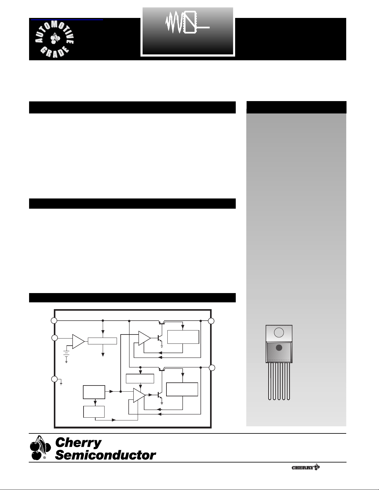
Description
V
IN
V
OUT
2
, 5V
Gnd
V
OUT
1
, 12V
ENABLE
+
-
Bandgap
Reference
+
-
+
-
Thermal
Shutdown
Over Voltage
Shutdown
Anti-Saturation
and
Current Limit
Anti-Saturation
and
Current Limit
Pre-Regulator
Block Diagram
Absolute Maximum Ratings
Input Voltage
Operating Range.....................................................................-0.5V to 26V
Peak Transient Voltage (Load Dump = 46V) ....................................60V
Internal Power Dissipation..................................................Internally Limited
Operating Temperature Range................................................-40¡C to +125¡C
Junction Temperature Range...................................................-40¡C to +150¡C
Storage Temperature Range ....................................................-65¡C to +150¡C
Lead Temperature Soldering
Wave Solder (through hole styles only)..........10 sec. max, 260¡C peak
The CS8156 is a low dropout 12V/5V
dual output linear regulator. The 12V
± 5% output sources 750mA and the 5V
±2.0% output sources 100mA.
The on board ENABLE function controls the regulatorÕs two outputs. When
the ENABLE lead is low, the regulator
is placed in SLEEP mode. Both outputs
are disabled and the regulator draws
only 200nA of quiescent current.
The regulator is protected against overvoltage conditions. Both outputs are
protected against short circuit and thermal runaway conditions.
The CS8156 is packaged in a 5 lead
TOÐ220 with copper tab. The copper
tab can be connected to a heat sink if
necessary.
1V
I
N
2V
OUT1
3 Gnd
4 ENABLE
5V
OUT2
A Company
¨
Rev. 2/19/98
Cherry Semiconductor Corporation
2000 South County Trail, East Greenwich, RI 02818
Tel: (401)885-3600 Fax: (401)885-5786
Email: info@cherry-semi.com
Web Site: www.cherry-semi.com
查询CS8156YT5供应商
Page 2

2
CS8156
PARAMETER TEST CONDITIONS MIN TYP MAX UNIT
Package Lead Description
PACKAGE LEAD # LEAD SYMBOL FUNCTION
5 Lead TO-220
1V
IN
Supply voltage, usually direct from battery.
2V
OUT1
Regulated output 12V, 750mA (typ)
3 Gnd Ground connection.
4 ENABLE CMOS compatible input lead; switches outputs on and off.
When ENABLE is high V
OUT1
and V
OUT2
are active.
5V
OUT2
Regulated output 5V, 100mA (typ).
Electrical Characteristics for V
OUT
: VIN= 14.5V, I
OUT1
= 5mA, I
OUT2
= 5mA, -40¡C ² TJ² +150ûC, -40¡C ² T
C
² +125ûC
unless otherwise specified
■ Output Stage(V
OUT1
)
Output Voltage, V
OUT1
13V ² V
IN
² 16V, I
OUT1
² 750mA 11.2 12.0 12.8 V
Dropout Voltage I
OUT1
= 500mA 0.4 0.6 V
I
OUT1
= 750mA 0.6 1.0 V
Line Regulation 13V ² V
IN
² 16V ,5mA ² I
OUT
< 100mA 15 80 mV
Load Regulation 5mA ² I
OUT1
² 500mA 15 80 mV
Quiescent Current I
OUT1
² 500mA, No Load on Standby 45 125 mA
I
OUT1
² 750mA, No Load on Standby 100 250 mA
Sleep Mode ENABLE = Low 200 nA
Ripple Rejection f = 120Hz, I
OUT
= 5mA, 42 70 dB
V
IN
= 1.5VPPat 15.5V
DC
Current Limit 0.75 1.20 2.50 A
Maximum Line Transient V
OUT1
² 13V 60 90 V
Reverse Polarity V
OUT1
³ -0.6V, 10½ Load -18 -30 V
Input Voltage, DC
Reverse Polarity Input 1% Duty Cycle, t = 100ms, V
OUT
³ -6V, -50 -80 V
Voltage, Transient 10½ Load
Output Noise Voltage 10Hz - 100kHz 500 µVrms
Output Impedance 500mA DC and 10mA rms, 100Hz 0.2 1.0 ½
Over-voltage Shutdown 28 34 45 V
■ Standby Output (V
OUT2
)
Output Voltage, (V
OUT2
) 9V ² V
IN
² 16V, 1mA ² I
OUT2
² 100mA 4.90 5.00 5.10 V
Dropout Voltage I
OUT2
² 100mA 0.60 V
Line Regulation 6V ² V
IN
² 26V; 1mA ² I
OUT
² 100mA 5 50 mV
Load Regulation 1mA ² I
OUT2
² 100mA; 9V ² V
IN
² 16V 5 50 mV
Quiescent Current V
OUT1
OFF, V
OUT2
OFF, V
ENABLE
= 0.8V 1 350 µA
Ripple Rejection f = 120Hz; I
OUT
= 100mA, 42 70 dB
V
IN
= 1.5VPPat 14.5V
DC
Current Limit 100 200 mA
■ ENABLE Function (ENABLE)
Input ENABLE Threshold V
OUT1
Off 1.25 0.80 V
V
OUT1
On 2.00 1.25 V
Input ENABLE Current V
ENABLE ²VTHRESHOLD
-10 0 10 µA
Page 3
3
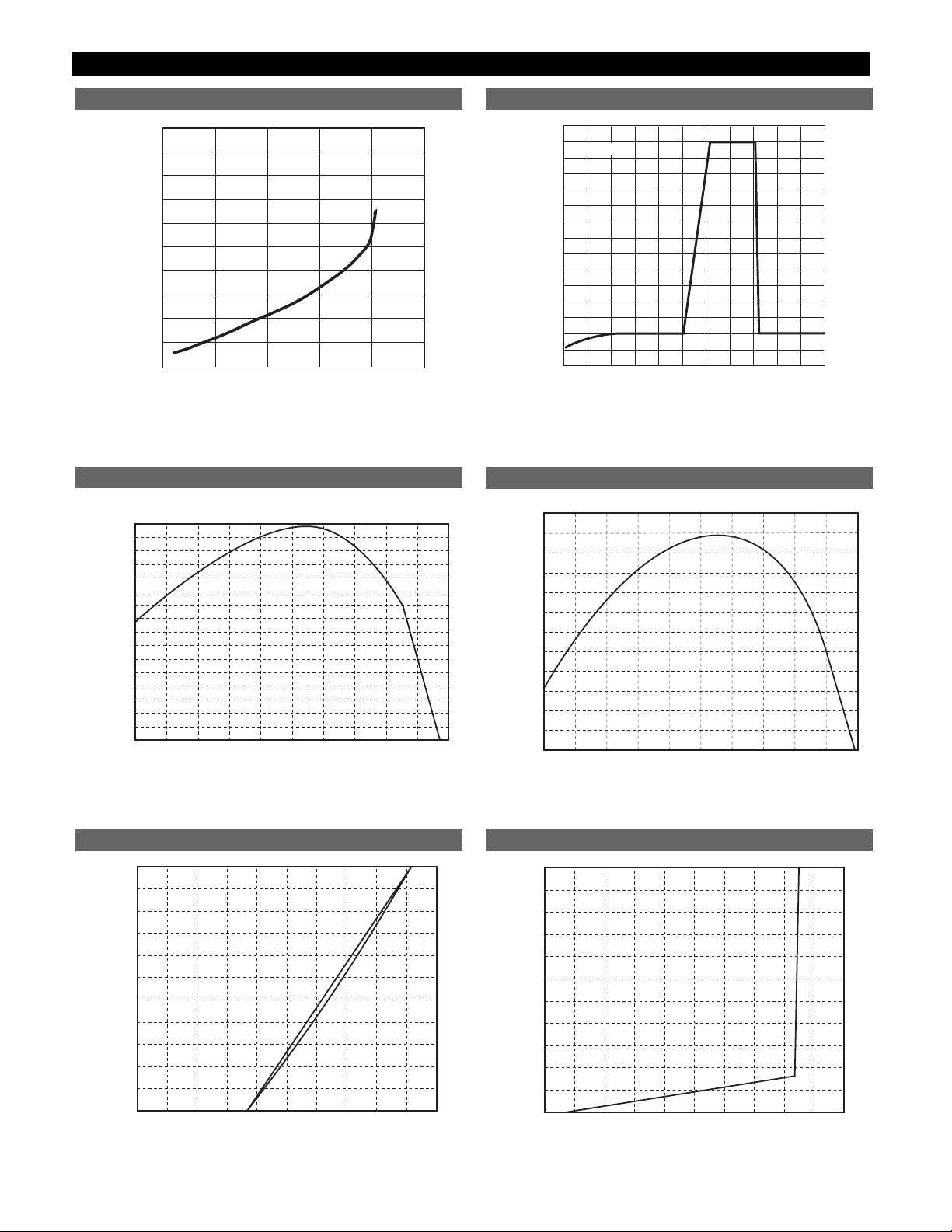
Typical Performance Characteristics
CS8156
0
0
50 100 150 200
Dropout Voltage (mV)
I
OUT
(mA)
200
400
600
800
1000
1200
1400
1600
1800
2000
Dropout Voltage vs I
OUT2
INPUT VOLTAGE (V)
OUTPUT VOLTAGE (V)
7
6
5
4
3
2
1
0
-1
-2
-40 -20 0 20 40 60
8
9
10
11
12
13
RL=10W
V
OUT1
vs. Input Voltage
-20
Temp (°C)
V
OUT
1
(V)
11.75
12.15
0 20 40 60 80 100 120 140 160-40
12.10
12.05
12.00
11.95
11.90
11.85
11.80
V
OUT1
vs. Temperature
-20
5.020
Temp (°C)
V
OUT
2
(V)
5.010
5.000
4.990
4.980
4.970
5.030
0 20 40 60 80 100 120 140 160-40
V
OUT2
vs. Temperature
V
ENABLE
(V)
I
ENABLE
(mA)
0
0
100
5
1234
20
40
60
80
ENABLE Current vs. ENABLE Voltage
V
ENABLE
(V)
I
ENABLE
(mA)
0.0
0.0
5.0
25
4.0
3.0
2.0
1.0
5101520
ENABLE Current vs. ENABLE Voltage
Page 4

4
CS8156
Typical Performance Characteristics: continued
20
10
0
-10
-20
3
2
1
0
TIME (ms)
INPUT VOLTAGE
CHANGE (V)
OUTPUT VOLTAGE
DEVIATION (mV)
I
OUT1
= 500mA
0 102030405060
Line Transient Response (V
OUT1
)
10
TIME (ms)
INPUT VOLTAGE
CHANGE (V)
OUTPUT VOLTAGE
DEVIATION (mV)
5
0
-5
-10
3
2
1
0
0 1020 3040 5060
I
OUT2
= 100mA
Line Transient Response (V
OUT2
)
150
TIME (ms)
LOAD
CURRENT (A)
OUTPUT VOLTAGE
DEVIATION (mV)
100
50
0
-50
-100
-150
0.8
0.6
0.4
0.2
0
0 102030405060
Load Transient Response (V
OUT1
)
150
TIME (ms)
STANDBY LOAD
CURRENT (mA)
STANDBY
OUTPUT VOLTAGE
DEVIATION (mV)
100
50
0
-50
-100
-150
20
15
10
5
0
0 102030405060
Load Transient Response (V
OUT2
)
AMBIENT TEMPERATURE (°C)
POWER DISSIPATION (W)
20
18
16
14
12
10
8
6
4
2
0
0 10 20 30 40 50 60 70 80 90
INFINITE
HEAT SINK
10°C/W HEAT SINK
NO HEAT SINK
Maximum Power Dissipation (TO-220)
150
140
130
120
110
90
80
70
60
50
40
30
20
10
100
0 100 200 300 400 500 600 700 800
125ûC
25ûC
-40ûC
No Load on 5V
V
IN
= 14V
0
Output Current (mA)
Quiescent Current (mA)
Quiescent Current vs Output Current for V
OUT2
Page 5

5
Typical Performance Characteristics: continued
Quiescent Current vs Output Current for V
OUT1
CS8156
Line Regulation vs Output Current for V
OUT1
Line Regulation vs Output Current for V
OUT2
Load Regulation vs Output Current for V
OUT1
Load Regulation vs Output Current for V
OUT2
22
No Load On 12V
20
18
16
14
VIN = 14V
12
10
8
6
Quiescent Current (mA)
4
-40ûC
25ûC
125ûC
0
0210
20 30 40 50 60 70 80 90 100 11 0 120 130 140 150
Output Current (mA)
-2
-4
-40ûC
25ûC
-6
-8
-10
-12
Load Regulation (mV)
-14
-16
-18
0
VIN = 14V
10020 30 40 50 60 70 80 90 100 11 0 120 130 140 150
125ûC
Output Current (mA)
2
1
0
-1
125ûC
-2
-40ûC
-3
Line Regulation (mV)
-4
-6
0-510320 30 40 50 60 70 80 90 100 11 0 120 130 140 150
VIN = 6 - 26V
Output Current (mA)
25
20
15
10
VIN = 13 - 26V
125ûC
5
0
-5
25ûC
-10
-15
-20
Line Regulation (mV)
-25
-30
-40ûC
-35
-40
0
100
100 100 100 100 100 100
Output Current (mA)
25ûC
800
0
-5
-10
-15
125ûC
-20
-25
VIN = 14V
-30
Load Regulation (mV)
-35
-40
0
100
200 300 400 500 600 700
Output Current (mA)
-40ûC
25ûC
800
Page 6

6
CS8156
V
IN
ENABLE
V
OUT
1
System
Condition
60V
3V
2.4V
12V
0V
Turn
On
Load
Dump
Low V
IN
Line Noise, Etc. V
OUT
1
Short
Circuit
V
OUT
1
Thermal
Shutdown
Turn
Off
5V
0V
14V
5V
2.0V
0.8V
14V
26V
31V
12V 12V
2.4V
12V12V
0V
0V
V
OUT
2
V
OUT
2
Short
Circuit
Typical Circuit Waveform
The output or compensation capacitor helps determine
three main characteristics of a linear regulator: start-up
delay, load transient response and loop stability.
The capacitor value and type should be based on cost,
availability, size and temperature constraints. A tantalum
or aluminum electrolytic capacitor is best, since a film or
ceramic capacitor with almost zero ESR can cause instability. The aluminum electrolytic capacitor is the cheapest
solution, but, if the circuit operates at low temperatures
(-25¡C to -40¡C), both the value and ESR of the capacitor
will vary considerably. The capacitor manufacturers data
sheet usually provides this information.
The value for the output capacitors C2 and C3 shown in
the test and applications circuit should work for most applications, however it is not necessarily the best solution.
To determine acceptable values for C2 and C3 for a particular application, start with a tantalum capacitor of the
recommended value and work towards a less expensive
alternative part for each output.
Step 1: Place the completed circuit with the tantalum
capacitors of the recommended value in an environmental
chamber at the lowest specified operating temperature
and monitor the outputs with an oscilloscope. A decade
box connected in series with capacitor C
2
will simulate the
higher ESR of an aluminum capacitor. Leave the decade
box outside the chamber, the small resistance added by
the longer leads is negligible.
Step 2: With the input voltage at its maximum value,
increase the load current slowly from zero to full load on
the output under observation. Look for any oscillations on
the output. If no oscillations are observed, the capacitor is
large enough to ensure a stable design under steady state
conditions.
Stability Considerations
Application Notes
Definition of Terms
Dropout Voltage
The input-output voltage differential at which the circuit
ceases to regulate against further reduction in input voltage.
Measured when the output voltage has dropped 100mV
from the nominal value obtained at 14V input, dropout voltage is dependent upon load current and junction temperature.
Input Voltage
The DC voltage applied to the input terminals with respect
to ground.
Input Output Differential
The voltage difference between the unregulated input voltage and the regulated output voltage for which the regulator
will operate.
Line Regulation
The change in output voltage for a change in the input voltage. The measurement is made under conditions of low dissipation or by using pulse techniques such that the average
chip temperature is not significantly affected.
Load Regulation
The change in output voltage for a change in load current at
constant chip temperature.
Long Term Stability
Output voltage stability under accelerated life-test conditions after 1000 hours with maximum rated voltage and
junction temperature.
Output Noise Voltages
The rms AC voltage at the output, with constant load and no
input ripple, measured over a specified frequency range.
Quiescent Current
The part of the positive input current that does not contribute to the positive load current. i.e., the regulator ground
lead current.
Ripple Rejection
The ratio of the peak-to-peak input ripple voltage to the
peak-to-peak output ripple voltage.
Temperature Stability of V
OUT
The percentage change in output voltage for a thermal variation from room temperature to either temperature extreme.
Page 7

7
Application Notes
Step 3: Increase the ESR of the capacitor from zero using
the decade box and vary the load current until oscillations
appear. Record the values of load current and ESR that
cause the greatest oscillation. This represents the worst
case load conditions for the output at low temperature.
Step 4: Maintain the worst case load conditions set in step
3 and vary the input voltage until the oscillations increase.
This point represents the worst case input voltage conditions.
Step 5: If the capacitor is adequate, repeat steps 3 and 4
with the next smaller valued capacitor. A smaller capacitor will usually cost less and occupy less board space. If
the output oscillates within the range of expected operating conditions, repeat steps 3 and 4 with the next larger
standard capacitor value.
Step 6: Test the load transient response by switching in
various loads at several frequencies to simulate its real
working environment. Vary the ESR to reduce ringing.
Step 7: Remove the unit from the environmental chamber
and heat the IC with a heat gun. Vary the load current as
instructed in step 5 to test for any oscillations.
Once the minimum capacitor value with the maximum
ESR is found for each output, a safety factor should be
added to allow for the tolerance of the capacitor and any
variations in regulator performance. Most good quality
aluminum electrolytic capacitors have a tolerance of +/20% so the minimum value found should be increased by
at least 50% to allow for this tolerance plus the variation
which will occur at low temperatures. The ESR of the
capacitors should be less than 50% of the maximum allowable ESR found in step 3 above.
Repeat steps 1 through 7 with C
3
, the capacitor on the
other output.
The maximum power dissipation for a dual output regulator (Figure 1) is:
P
D(max)
= {V
IN(max)ÐVOUT1(min)}IOUT1(max)
+
{V
IN(max)ÐVOUT2(min)}IOUT2(max)+VIN(max)IQ
(1)
Where:
V
IN(max)
is the maximum input voltage,
V
OUT1(min)
is the minimum output voltage from V
OUT1
,
V
OUT2(min)
is the minimum output voltage fromV
OUT2
,
I
OUT1(max)
is the maximum output current for the appli-
cation,
I
OUT2(max)
is the maximum output current for the appli-
cation, and
IQis the quiescent current the regulator consumes at
I
OUT(max)
.
Once the value of P
D(max)
is known, the maximum permis-
sible value of R
QJA
can be calculated:
R
QJA
=
(2)
Figure 1: Dual output regulator with key performance parameters
labeled.
The value of R
QJA
can then be compared with those in
the package section of the data sheet. Those packages
with R
QJA
's less than the calculated value in equation 2
will keep the die temperature below 150¡C.
In some cases, none of the packages will be sufficient to
dissipate the heat generated by the IC, and an external
heatsink will be required.
A heat sink effectively increases the surface area of the
package to improve the flow of heat away from the IC and
into the surrounding air.
Each material in the heat flow path between the IC and the
outside environment will have a thermal resistance. Like
series electrical resistances, these resistances are summed
to determine the value of R
QJA
:
R
QJA
= R
QJC
+ R
QCS
+ R
QSA
(3)
where
R
QJC
= the junctionÐtoÐcase thermal resistance,
R
QCS
= the caseÐtoÐheatsink thermal resistance, and
R
QSA
= the heatsinkÐtoÐambient thermal resistance.
R
QJC
appears in the package section of the data sheet. Like
R
QJA
, it too is a function of package type. R
QCS
and R
QSA
are functions of the package type, heatsink and the interface between them. These values appear in heat sink data
sheets of heat sink manufacturers.
C1*
0.1mF
+
C2**
22mF
+
C3**
22mF
V
IN
ENABLE
V
OUT1
V
OUT2
Gnd
CS8156
Test & Application Circuit
Heat Sinks
150¡C - T
A
P
D
Calculating Power Dissipation
in a Dual Output Linear Regulator
NOTES:
*C
1
required if regulator is located far
from power supply filter.
** C
2
, C3required for stability.
CS8156
I
IN
V
IN
Regulator
Control
Features
}
Smart
I
Q
I
I
OUT
OUT
1
V
OUT
1
2
V
OUT
2
Page 8

Part Number Description
CS8156YT5 5 Lead TO-220 Straight
CS8156YTVA5 5 Lead TO-220 Vertical
CS8156YTHA5 5 Lead TO-220 Horizontal
8
CS8156
Rev. 2/19/98
Ordering Information
Package Specification
Thermal Data 5 Lead TO-220
R
QJC
typ 2.0 ûC/W
R
QJA
typ 50 ûC/W
PACKAGE THERMAL DATA
PACKAGE DIMENSIONS IN mm(INCHES)
© 1999 Cherry Semiconductor Corporation
Cherry Semiconductor Corporation reserves the
right to make changes to the specifications without
notice. Please contact Cherry Semiconductor
Corporation for the latest available information.
5 Lead TO-220 (T) Straight
2.87 (.113)
2.62 (.103)
6.93(.273)
6.68(.263)
9.78 (.385)
10.54 (.415)
1.02(.040)
0.63(.025)
1.83(.072)
1.57(.062)
0.56 (.022)
0.36 (.014)
2.92 (.115)
2.29 (.090)
1.40 (.055)
1.14 (.045)
4.83 (.190)
4.06 (.160)
6.55 (.258)
5.94 (.234)
14.22 (.560)
13.72 (.540)
1.02 (.040)
0.76 (.030)
3.71 (.146)
3.96 (.156)
14.99 (.590)
14.22 (.560)
5 Lead TO-220 (THA) Horizontal
0.81(.032)
1.70 (.067)
6.81(.268)
1.40 (.055)
1.14 (.045)
5.84 (.230)
6.60 (.260)
6.83 (.269)
0.56 (.022)
0.36 (.014)
10.54 (.415)
9.78 (.385)
6.55 (.258)
5.94 (.234)
3.96 (.156)
3.71 (.146)
1.68
(.066)
TYP
14.99 (.590)
14.22 (.560)
2.77 (.109)
2.29 (.090)
2.92 (.115)
4.83 (.190)
4.06 (.160)
2.87 (.113)
2.62 (.103)
5 Lead TO-220 (TVA) Vertical
1.68
(.066) typ
1.70 (.067)
7.51 (.296)
1.78 (.070)
4.34 (.171)
0.56 (.022)
0.36 (.014)
1.40 (.055)
1.14 (.045)
4.83 (.190)
4.06 (.160)
14.99 (.590)
14.22 (.560)
2.92 (.115)
2.29 (.090)
.94 (.037)
.69 (.027)
8.64 (.340)
7.87 (.310)
6.80 (.268)
10.54 (.415)
9.78 (.385)
2.87 (.113)
2.62 (.103)
6.55 (.258)
5.94 (.234)
3.96 (.156)
3.71 (.146)
 Loading...