

Datasheet CS8151YTVA7, CS8151YT7, CS8151YNF16, CS8151YDWFR16, CS8151YDWF16 Datasheet (Cherry Semiconductor)
...Page 1
5V, 100mA Low Dropout Linear Regulator
with WATCHDOG, RESET, & WAKE UP
The CS8151 is a precision 5V, 100mA
micro-power voltage regulator with
very low quiescent current (400µA
typical at 200µA load). The 5V output
is accurate within ±2% and supplies
100 mA of load current with a typical
dropout voltage of 400mV.
Microprocessor control logic includes
Watchdog, Wake Up and . This
unique combination of low quiescent
current and full microprocessor control makes the CS8151 ideal for use in
battery operated, microprocessor controlled equipment.
The CS8151 WAKE UP function brings
the microprocessor out of Sleep mode.
The microprocessor in turn, signals its
WAKE UP status back to the CS8151
by issuing a WATCHDOG signal.
The WATCHDOG logic function monitors an input signal (WDI) from the
microprocessor. The CS8151 responds
to the falling edge of the WATCHDOG signal which it expects at least
once during each wake-up period.
When the correct WATCHDOG signal
is received, a falling edge is issued on
the wake-up signal line.
is independent of V
IN
and
operates correctly to an output voltage
as low as 1V. A signal is issued
in any of three situations. During
power up the is held low until
the output voltage is in regulation.
During operation if the output voltage
shifts below the regulation limits, the
toggles low and remains low
until proper output voltage regulation
is restored. And finally, a signal
is issued if the regulator does not
receive a WATCHDOG signal within
the WAKE UP period.
The pulse width, WAKE UP
signal frequency, and WAKE UP delay
time are all set by one external capacitor C
Delay
.
The regulator is protected against
short circuit, over voltage, and thermal
runaway conditions. The device can
withstand 74 volt load dump transients, making it suitable for use in
automotive environments.
RESET
RESET
RESET
RESET
RESET
RESET
RESET
1
Features
■
5V ±2% / 100 mA Output
Voltage
■
Micropower Compatible
Control Functions:
WAKE UP
WATCHDOG
■
Low Dropout Voltage:
400mV @ 100mA
■
Low Sleep Mode Quiescent
Current (400µA typ)
■
Protection Features:
Thermal Shutdown
Short Circuit
74V Load Dump
Reverse Transient (-50V)
RESET
Package Options
16 Lead PDIP
16 Lead SOIC Wide*
(Internally Fused)
CS8151
N/C
N/C
N/C
N/C
Gnd
Gnd
Gnd
Gnd
Sense
V
OUT
Delay
______
RESET
WAKE UP
WDI
V
IN
*N/C
* For SO Wide package, pin # 6 is Gnd
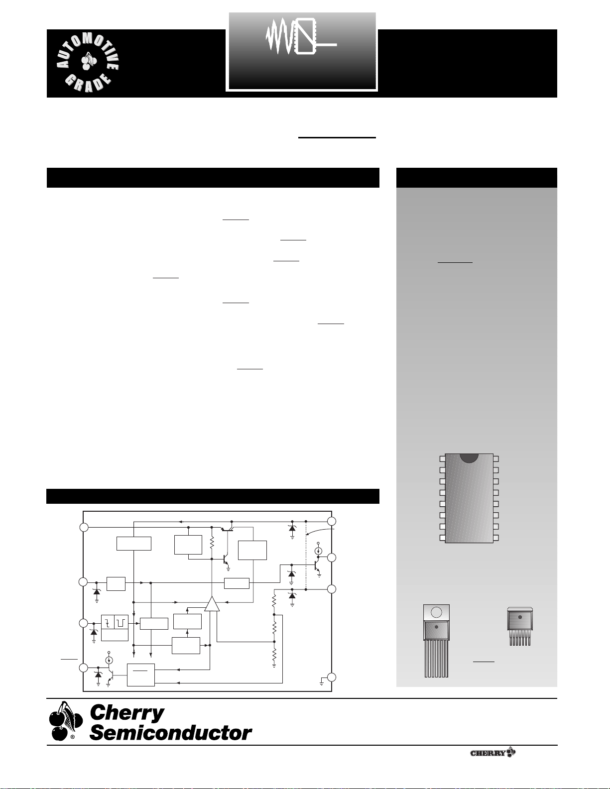
CS8151
Description
Block Diagram
7 Lead TO-220
Tab (Gnd)
7 Lead D2PAK
Tab (Gnd)
1
1. V
OUT
2. V
IN
3. WDI
4. Gnd
5. WAKE UP
6.
7. Delay
RESET
A Company
¨
Rev. 5/4/99
Cherry Semiconductor Corporation
2000 South County Trail, East Greenwich, RI 02818
Tel: (401)885-3600 Fax: (401)885-5786
Email: info@cherry-semi.com
Web Site: www.cherry-semi.com
1
V
IN
Delay
WDI
RESET
Timing
Circuit
Falling Edge
Detector
V
OUT
Current Source
(Circuit Bias)
WATCHDOG
RESET
Circuit
Voltage
Shutdown
Thermal
Shutdown
Circuit
Bandgap
Reference
Over
+ -
WAKE UP
Circuit
Error
Amplifier
Current Limit
Sense
V
OUT
internally
connected on
V
TO-220 and
OUT
D2PAK
WAKE UP
Sense
Gnd
Page 2
2
PARAMETER TEST CONDITIONS MIN TYP MAX UNIT
Absolute Maximum Ratings
Power Dissipation.............................................................................................................................................Internally Limited
Output Current (V
OUT
, , WAKE UP) .................................................................................................Internally Limited
Reverse Battery..........................................................................................................................................................................-15V
Maximum Load Dump Transient .........................................................................................................................................+74V
Maximum Negative Transient (t<2ms) .................................................................................................................................-50V
ESD Susceptibility (Human Body Model)..............................................................................................................................2kV
ESD Susceptibility (Machine Model).....................................................................................................................................200V
Logic Inputs/Outputs ................................................................................................................................................-0.3V to +6V
Storage Temperature Range................................................................................................................................-55¡C to +150¡C
Lead Temperature Soldering
Wave Solder (through hole styles only) .....................................................................................10 sec. max, 260¡C peak
Reflow (SMD styles only) ......................................................................................60 sec. max above 183¡C, 230¡C peak
RESET
CS8151
Electrical Characteristics: TA = -40¡C to +125¡C, -40¡C ² TJ ² 150¡C, 6V ² V
IN
² 26V, I
OUT
= 100µA to 100mA, C2 = 47µF
(ESR < 8½), C
Delay
= 0.1µF (unless otherwise noted)
■ Output Section
Output Voltage, V
OUT
9V < VIN< 16V 4.90 5.00 5.10 V
6V < VIN< 26V, 0 < I
OUT
< 100mA 4.85 5.00 5.15 V
Dropout Voltage (VIN- V
OUT
)I
OUT
= 100mA 400 600 mV
I
OUT
= 100µA 100 150 mV
Load Regulation VIN= 14V, 100µA < I
OUT
< 100mA 10 50 mV
Line Regulation I
OUT
= 1mA, 6V < V
IN
< 26V 10 50 mV
Ripple Rejection 7V < V
IN
< 17V @ f = 120Hz, 60 75 dB
I
OUT
= 100mA
Current Limit V
OUT
= 4.5V 100 250 mA
Thermal Shutdown 150 180 210 ¡C
Overvoltage Shutdown V
OUT
< 1V 50 56 62 V
Quiescent Current I
OUT
= 200µA (Sleep) 0.40 0.75 mA
I
OUT
= 50mA 4 mA
I
OUT
= 100mA (WAKE UP) 12 20 mA
Reverse Current V
OUT
= 5V, VIN= 0V 1.0 1.5 mA
■
Threshold High (RTH) RTH V
OUT
Increasing V
OUT
- 0.3 V
OUT
- 0.04 V
Threshold Low (RTL) RTL V
OUT
Decreasing 4.50 4.70 4.91 V
Hysteresis RTH Ð RTL 150 200 250 mV
Output
LOW 1V < V
OUT
< RTL, I
OUT
= 25µA 0.2 0.8 V
HIGH I
OUT
= 25µA, V
OUT
> RTH 3.8 4.2 5.1 V
Current Limit = 0V, V
OUT
> V
RTH
(sourcing) 0.025 0.50 1.30 mA
= 5V, V
OUT
> 1V (sinking) 0.1 12 80 mA
Delay Time POR Mode 3 5 7 ms
RESET
RESET
RESET
Page 3
3
Package Lead Description
Package Lead # Lead Symbol Function
Electrical Characteristics: continued
PARAMETER TEST CONDITIONS MIN TYP MAX UNIT
CS8151
■ WATCHDOG Input
Threshold
HIGH 1.4 2.0 V
LOW 0.8 1.3 V
Hysteresis 25 100 mV
Input Current 0 < WDI < 6V -10 0 +10 µA
Pulse Width 50% WDI falling edge to 5 µs
50% WDI rising edge and
50% WDI rising edge to 50%
WDI falling edge (see Figure 1)
■ WAKE UP Output
WAKE UP Period see Figure 1a 30 40 50 ms
WAKE UP Duty Cycle nominal see Figure 1c 40 50 60 %
HIGH to WAKE UP 50% rising edge to 15 20 25 ms
Rising Delay Time 50% WAKE UP edge
(see Figure 1)
WAKE UP Response 50% WDI falling edge to 2 10 µs
to Watchdog Input 50% WAKE UP falling edge
WAKE UP Response 50% falling edge to 2 10 µs
to 50% WAKE UP falling edge
V
OUT
= 5V®4.5V
Output
LOW I
OUT
= 25µA(sinking) 0.2 0.8 V
HIGH I
OUT
= 25µA(sourcing) 3.8 4.2 5.1 V
Current Limit WAKE UP = 5V 0.025 1.00 7.00 mA
WAKE UP = 0V .05 3.50 mA
RESET
RESET
RESETRESET
7L TO-220 & 16 L PDIP 16L SOIC
7L D
2
PAK (internally fused) (internally fused)
299V
IN
Supply voltage to the IC.
3 11 11 WDI CMOS/TTL compatible input lead. The watchdog function
monitors the falling edge of the incoming signal.
4 4,5,12,13 4,5,6,12,13 Gnd Ground Connection
7 16 16 Delay Input lead from timing capacitor for and WAKE UP
signal.
6 15 15 CMOS/TTL compatible output lead goes low when-
ever V
OUT
drops by more than 6% from nominal, or during
the absence of a correct watchdog signal.
5 14 14 WAKE UP CMOS/TTL compatible output consisting of a continuously
generated signal used to WAKE UP the microprocessor from
sleep mode.
188V
OUT
Regulated output voltage 5V ± 2%.
7 7 Sense Kelvin connection which allows remote sensing of the output
voltage for improved regulation. If remote sensing is not
required, connect to V
OUT
.
RESETRESET
RESET
Page 4

4
Timing Diagrams
Figure 1c. Power Down and Restart Sequence
Figure 1b. Error Condition: Watchdog remains LOW and a is issued
RESET
______
RESET
WAKE UP
WDI
V
OUT
-
POR
V
IN
______
RESET High
to Wakeup
Delay Time
Power Up Sleep Mode
Normal Operation with varying WATCHDOG Signal
WAKE UP Duty Cycle = 50%
Figure 1a. Power Up, Sleep Mode and Normal Operation
CS8151
______
V
IN
______
RESET
WAKE UP
WDI
V
OUT
______
RESET
WAKE UP
WDI
V
OUT
POR
______
RESET HIGH
to WAKE UP
DELAY TIME
POR
WAKE UP
period
WATCHDOG Pulse Width
RESET delay time
______
RESET HIGH
to WAKEUP
DELAY TIME
RTL
POWER DOWN
WAKE UP period
POR
Page 5

5
To reduce the drain on the battery a system can go into a
low current consumption mode when ever its not performing a main routine. The WAKE UP signal is generated
continuously and is used to interrupt a microcontroller
that is in sleep mode. The nominal output is a 5 volt
square wave with a duty cycle of 50% at a frequency that
is determined by a timing capacitor, C
Delay
.
When the microprocessor receives a rising edge from the
WAKE UP output, it must issue a watchdog pulse and
check its inputs to decide if it should resume normal operations or remain in the sleep mode.
The first falling edge of the watchdog signal causes the
WAKE UP to go low within 2µs (typ) and remain low until
the next WAKE UP cycle (see Figure 2). Other watchdog
pulses received within the same cycle are ignored (Figure
1).
During power up, is held low until the output voltage is in regulation. During operation, if the output voltage shifts below the regulation limits, the RESET toggles
low and remains low until proper output voltage regulation is restored. After the delay, returns
high.
The WATCHDOG circuitry continuously monitors the
input watchdog signal (WDI) from the microprocessor.
The absence of a falling edge on the WATCHDOG input
during one WAKE UP cycle will cause a pulse to
occur at the end of the WAKE UP cycle. (see Figure 1b).
The WAKE UP output is pulled low during a
regardless of the cause of the . After the
returns high, the WAKE UP cycle begins again (see
Figures 1b).
The pulse width, WAKE UP signal frequency and
high to WAKE UP delay time are all set by one
external capacitor C
Delay
.
WAKE UP period=(4x10⁵)C
Delay
Delay Time=(5x10⁴)C
Delay
HIGH to WAKE UP Delay Time =(2x10⁵)C
Delay
Capacitor temperature coefficient and tolerance as well as the
tolerance of the CS8151 must be taken into account in order
to get the correct system tolerance for each parameter.
Figure 2. WAKE UP response to WDI
Figure 3. WAKE UP response to (Low Voltage)
RESET
WAKE UP
Response to
______
RESET
______
RESET
WAKE UP
WAKE UP
Response to
WDI
WAKE UP
WDI
RESET
RESET
RESET
RESET
RESETRESET
RESET
RESET
RESETRESET
RESET
Dropout Voltage:
The input-output voltage differential at which the circuit ceases to regulate against further reduction in
input voltage. Measured when the output voltage has
dropped 100mV from the nominal value obtained at
14V input, dropout voltage is dependent upon load
current and junction temperature.
Input Voltage:
The DC voltage applied to the input terminals with
respect to ground.
Line Regulation:
The change in output voltage for a change in the
input voltage. The measurement is made under conditions of low dissipation or by using pulse techniques such that the average chip temperature is not
significantly affected.
Load Regulation:
The change in output voltage for a change in load
current at constant chip temperature.
Quiescent Current:
The part of the positive input current that does not
contribute to the positive load current. The regulator
ground lead current.
Ripple Rejection:
The ratio of the peak-to-peak input ripple voltage to
the peak-to-peak output ripple voltage.
Current Limit:
Peak current that can be delivered to the output.
Definition of Terms
Circuit Description
CS8151
Functional Description
Page 6

The output stage is protected against overvoltage, short
circuit and thermal runaway conditions (see Figure 4).
Figure 4: Typical Circuit Waveforms for Output Stage Protection.
If the input voltage rises above 56V (e.g. load dump), the
output shuts down. This response protects the internal circuitry and enables the IC to survive unexpected voltage
transients.
Should the junction temperature of the power device
exceed 180ûC (typ) the power transistor is turned off.
Thermal shutdown is an effective means to prevent die
overheating since the power transistor is the principle heat
source in the IC.
The output or compensation capacitor C
2
(see Figure 5)
helps determine three main characteristics of a linear regulator: start-up delay, load transient response and loop stability.
Figure 5. Test and application circuit showing output compensation.
The capacitor value and type should be based on cost,
availability, size and temperature constraints. A tantalum
or aluminum electrolytic capacitor is best, since a film or
ceramic capacitor with almost zero ESR can cause instability. The aluminum electrolytic capacitor is the least expensive solution, but, if the circuit operates at low temperatures (-25¡C to -40¡C), both the value and ESR of the
capacitor will vary considerably. The capacitor manufacturers data sheet usually provide this information.
The value for the output capacitor C2shown in the test
and applications circuit should work for most applications, however it is not necessarily the optimized solution.
To determine an acceptable value for C
2
for a particular
application, start with a tantalum capacitor of the recommended value and work towards a less expensive
alternative part.
Step 1: Place the completed circuit with a tantalum capacitor of the recommended value in an environmental chamber at the lowest specified operating temperature and
monitor the outputs with an oscilloscope. A decade box
connected in series with the capacitor will simulate the
higher ESR of an aluminum capacitor. Leave the decade
box outside the chamber, the small resistance added by the
longer leads is negligible.
Step 2: With the input voltage at its maximum value,
increase the load current slowly from zero to full load
while observing the output for any oscillations. If no oscillations are observed, the capacitor is large enough to
ensure a stable design under steady state conditions.
Step 3: Increase the ESR of the capacitor from zero using
the decade box and vary the load current until oscillations
appear. Record the values of load current and ESR that
cause the greatest oscillation. This represents the worst
case load conditions for the regulator at low temperature.
Step 4: Maintain the worst case load conditions set in step
3 and vary the input voltage until the oscillations increase.
This point represents the worst case input voltage conditions.
Step 5: If the capacitor is adequate, repeat steps 3 and 4
with the next smaller valued capacitor. A smaller capacitor
will usually cost less and occupy less board space. If the
output oscillates within the range of expected operating
conditions, repeat steps 3 and 4 with the next larger standard capacitor value.
Step 6: Test the load transient response by switching in
various loads at several frequencies to simulate its real
working environment. Vary the ESR to reduce ringing.
Step 7: Remove the unit from the environmental chamber
and heat the IC with a heat gun. Vary the load current as
instructed in step 5 to test for any oscillations.
Once the minimum capacitor value with the maximum
ESR is found, a safety factor should be added to allow for
the tolerance of the capacitor and any variations in regulator performance. Most good quality aluminum electrolytic
capacitors have a tolerance of ±20% so the minimum value
found should be increased by at least 50% to allow for this
tolerance plus the variation which will occur at low temperatures. The ESR of the capacitor should be less than
50% of the maximum allowable ESR found in step 3 above.
The maximum power dissipation for a single output regulator (Figure 6) is:
P
D(max)
= {V
IN(max)
Ð V
OUT(min)
}
I
OUT(max)
+ V
IN(max)IQ
(1)
where:
V
IN(max)
is the maximum input voltage,
V
OUT(min)
is the minimum output voltage,
I
OUT(max)
is the maximum output current for the applica-
tion, and
IQis the quiescent current the regulator consumes at
I
OUT(max)
.
Calculating Power Dissipation
in a Single Output Linear Regulator
Stability Considerations
I
OUT
V
OUT
V
IN
Load
Dump
Short
Circuit
Thermal
Shutdown
> 30V
Output Stage Protection
CS8151
Application Notes
*C1required if regulator is located
far from the power supply filter.
**C
2
required for stability.
6
V
IN
C1*
0.1mF
CS8151
V
OUT
RESET
R
RST
C2**
10mF
Page 7

7
Once the value of P
D(max)
is known, the maximum permis-
sible value of R
QJA
can be calculated:
R
QJA
=
(2)
The value of R
QJA
can then be compared with those in
the package section of the data sheet. Those packages with
R
QJA
's less than the calculated value in equation 2 will
keep the die temperature below 150¡C.
In some cases, none of the packages will be sufficient to
dissipate the heat generated by the IC, and an external
heatsink will be required.
A heat sink effectively increases the surface area of the
package to improve the flow of heat away from the IC and
into the surrounding air.
Each material in the heat flow path between the IC and
the outside environment will have a thermal resistance.
Like series electrical resistances, these resistances are
summed to determine the value of R
QJA
:
R
QJA
= R
QJC
+ R
QCS
+ R
QSA
(3)
where:
R
QJC
= the junctionÐtoÐcase thermal resistance,
R
QCS
= the caseÐtoÐheatsink thermal resistance, and
R
QSA
= the heatsinkÐtoÐambient thermal resistance.
R
QJC
appears in the package section of the data sheet. Like
R
QJA
, it too is a function of package type. R
QCS
and R
QSA
are functions of the package type, heatsink and the interface between them. These values appear in heat sink data
sheets of heat sink manufacturers.
150¡C - T
A
P
D
Application Diagram
CS8151
Heat Sinks
Figure 6. Single output regulator with key performance parameters
labeled.
Application Diagram
I
IN
V
IN
Regulator
Control
Features
}
Smart
I
Q
I
OUT
V
OUT
BATTERY
V
C
Delay
IN
C
CS8151
Delay
Gnd
C
1
V
WDI
______
RESET
WAKE UP
OUT
V
CC
C
2
Microprocessor
I/O
______
RESET
I/O
Page 8

Thermal Data 7 Lead 7 Lead 16 Lead 16 Lead
TO-220 D2PAK PDIP SOIC Wide
R
QJC
typ 1.8 1.8 15 18 ûC/W
R
QJA
typ 50 10-50* 50 75 ûC/W
*Depending on thermal properties of substrate. R
QJA
= R
QJC
+ R
QCA
D
Lead Count Metric English
Max Min Max Min
16L PDIP (Internally Fused Leads) 19.69 18.67 .775 .735
16L SOIC Wide 10.50 10.10 .413 .398
(Internally Fused Leads)
8
Package Specification
PACKAGE DIMENSIONS IN mm (INCHES)
Ordering Information
PACKAGE THERMAL DATA
Rev. 5/4/99
Part Number Description
CS8151YT7 7 lead TO-220 Straight
CS8151YTVA7 7 lead TO-220 Vertical
CS8151YDPS7 7 lead D2PAK Short-Leaded
CS8151YDPSR7 7 lead D
2
PAK Short-Leaded
(tape & reel)
CS8151YNF16 16 lead PDIP (Internally Fused Leads)
CS8151YDWF16 16 lead SOIC Wide
(Internally Fused Leads)
CS8151YDWFR16 16 lead SOIC Wide
(Internally Fused Leads) (tape & reel)
CS8151
© 1999 Cherry Semiconductor Corporation
Cherry Semiconductor Corporation reserves the
right to make changes to the specifications without
notice. Please contact Cherry Semiconductor
Corporation for the latest available information.
Plastic DIP (N); 300 mil wide
0.39 (.015)
MIN.
2.54 (.100) BSC
1.77 (.070)
1.14 (.045)
D
Some 8 and 16 lead
packages may have
1/2 lead at the end
of the package.
All specs are the same.
.203 (.008)
.356 (.014)
REF: JEDEC MS-001
3.68 (.145)
2.92 (.115)
8.26 (.325)
7.62 (.300)
7.11 (.280)
6.10 (.240)
.356 (.014)
.558 (.022)
Surface Mount Wide Body (DW); 300 mil wide
1.27 (.050) BSC
7.60 (.299)
7.40 (.291)
10.65 (.419)
10.00 (.394)
D
0.32 (.013)
0.23 (.009)
1.27 (.050)
0.40 (.016)
REF: JEDEC MS-013
2.49 (.098)
2.24 (.088)
0.51 (.020)
0.33 (.013)
2.65 (.104)
2.35 (.093)
0.30 (.012)
0.10 (.004)
7 Lead TO-220 (T) Straight
2.87 (.113)
2.62 (.103)
9.78 (.385)
10.54 (.415)
1.40 (.055)
1.14 (.045)
0.64 (.025)
0.38 (.015)
0.56 (.022)
0.36 (.014)
1.40 (.055)
1.14 (.045)
4.83 (.190)
4.06 (.160)
14.22 (.560)
13.72 (.540)
0.94 (.037)
0.58 (.023)
7.75 (.305)
7.49 (.295)
2.92 (.115)
2.29 (.090)
3.71 (.146)
3.96 (.156)
14.99 (.590)
14.22 (.560)
6.55 (.258)
5.94 (.234)
7 Lead D2PAK (DPS)* Short-Leaded
1.98 (.078)
1.47 (.058)
14.71 (.579)
13.69 (.539)
4.57 (.180)
4.31 (.170)
1.40 (.055)
1.14 (.045)
2.79 (.110)
2.54 (.100)
TERMINAL 8
7.75 (.305)
REF
6.50 (.256) REF
10.31 (.406)
10.05 (.396)
1.27 (.050)
REF
1.68 (.066)
1.40 (.055)
.254 (.010)
REF
0.91 (.036)
0.66 (.026)
8.53 (.336)
8.28 (.326)
0.10 (.004)
0.00 (.000)
*CHERRY SEMICONDUCTOR SHORT-LEADED FOOTPRINT
 Loading...