

Page 1
1
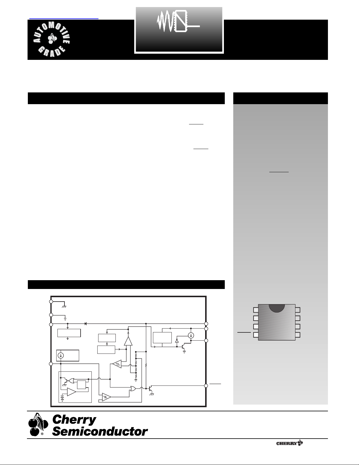
The CS8127 contains all the necessary
control circuitry to implement a 5V linear regulator. An external pass device is
used to produce superior performance
compared to conventional monolithic
regulators. The CS8127 with a TIP42
PNP transistor typically provides a
100mV dropout voltage at 500mA,
increasing to 350mV at 3A. Quiescent
current at 500mA is only 5mA.
Monolithic regulators cannot approach
these figures because their power transistors do not provide the high beta and
excellent saturation characteristics at
high currents. The CS8127 is compatible
with a wide variety of external transistors, allowing flexibility for thermal,
space, and cost management.
The CS8127 includes thermal shutdown,
externally programmable current limit,
and over-voltage shutdown, making it
suitable for use in automotive and
switching regulator post regulator applications. An optional external RC filter
added to the CS8127 supply lead provides EMC hardening in addition to the
on-chip EMC hardening. The SENSE
lead allows remote sensing of the output
voltage for improved regulation.
An active microprocessor RESET function is included on-chip with externally
programmable delay time. During
power-up, or after detection of any error
in the regulated output, the RESET lead
will remain in the low state for the duration of the delay. Types of errors include
short circuit, low input voltage, overvoltage shutdown, thermal shutdown,
or others that cause the output to
become unregulated. This function is
independent of the input voltage and
will function correctly with an output
voltage as low as 1V. Hysteresis is
included in both the reset and delay
comparators for noise immunity and to
prevent oscillations. A latching discharge circuit is used to discharge the
delay capacitor, even when triggered by
a relatively short fault condition. This
circuit improves upon the commonly
used SCR structure by providing
improved noise immunity and full
capacitor discharge (0.2V typ).
Features
■ Externally Set Delay for
Reset
■ 60V Peak Transient
Capability
■ Internal Thermal
Overload Protection
■ 3% Output Accuracy
■ Active RESET
■ Noise Immunity
■ On Chip EMC Hardening
Protection Incorporated
■ Externally Set Current
Limit
Package Options
8L SO & 8L PDIP
CS8127
5V Linear Controller/Driver
1
V
IN
2
3
4
Sense
Delay
V
OUT
Pwr Gnd
Pullup
Ref Gnd
8
7
6
5
RESET
CS8127
Description
Block Diagram
A Company
¨
Rev. 2/12/99
Cherry Semiconductor Corporation
2000 South County Trail, East Greenwich, RI 02818
Tel: (401)885-3600 Fax: (401)885-5786
Email: info@cherry-semi.com
Web Site: www.cherry-semi.com
查询CS8127YD8供应商
Pwr Gnd
Ref Gnd
V
IN
Delay
IC
Power
Gnd
IC
Reference
Gnd
PRE-
REGULATOR
Regulated Supply
for Circuit Bias
10mA
Delay
Current
Latching
Discharge
-
+
V
dis
Q
S
R
Thermal
Shutdown
Bandgap
Reference
Delay
Comparator
-
+
Reset
Comparator
1.25V
Error
Amp
+
-
+
-
Over
Voltage
Shutdown
50mA
Sense
PULLUP
V
OUT
RESET
Page 2
2
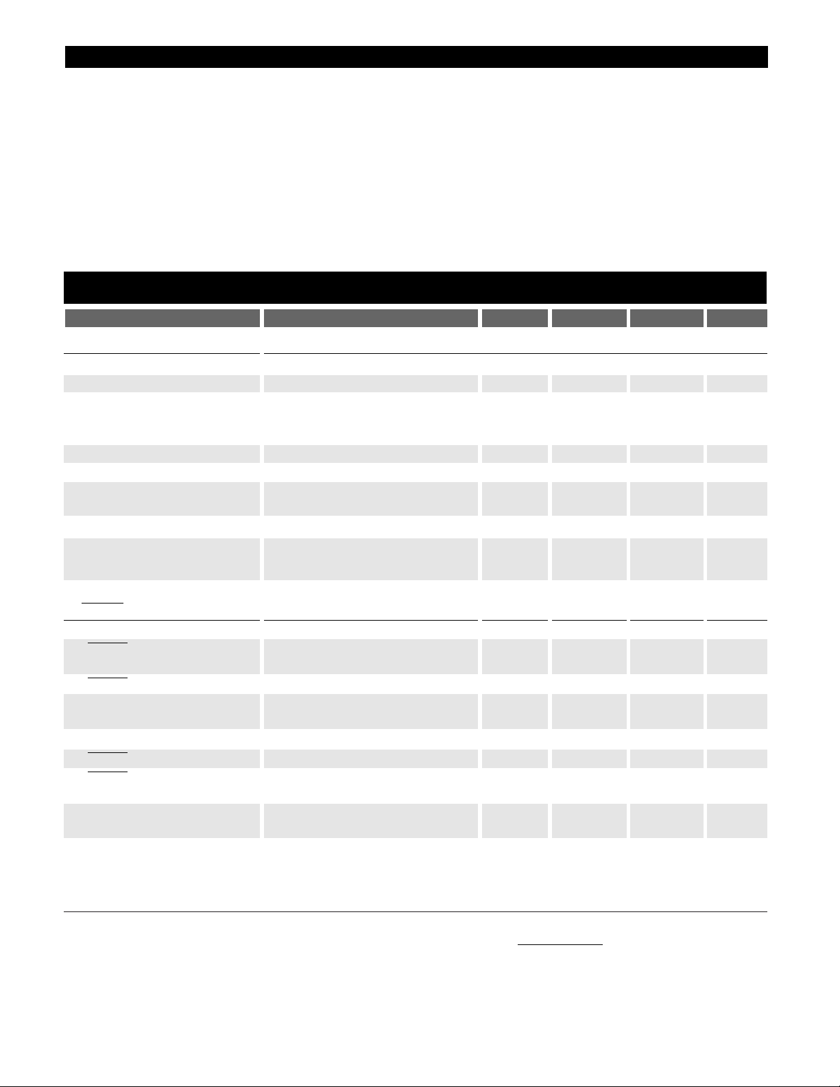
Note 1: Dependent on characteristics of external transistor.
Electrical Characteristics: T
A
=-40ûC to +125ûC, TJ=-40ûC to +150ûC, VIN=6 to 26V, I
OUT
=5 to 500mA, Per Test Circuit
(unless otherwise noted)
PARAMETER TEST CONDITIONS MIN TYP MAX UNIT
Absolute Maximum Ratings
Power Dissipation.............................................................................................................................................Internally Limited
Input Voltage ..................................................................................................................................................................Ð0.3V, 26V
Transient Input Voltage ............................................................................................................................................................60V
Output Current ...............................................................................................................................................Externally Limited
ESD Susceptibility (Human Body Model)..............................................................................................................................2kV
Junction Temperature ............................................................................................................................................Ð45¡C to 150¡C
Storage Temperature..............................................................................................................................................Ð55¡C to 150¡C
Lead Temperature Soldering
Wave Solder (through hole styles only) .....................................................................................10 sec. max, 260¡C peak
Reflow (SMD styles only) ......................................................................................60 sec. max above 183¡C, 230¡C peak
CS8127
C
Delay
x V
DTC
I
Charge
Note 2: Delay Time =
= C
Delay
x 3.5 x 10⁵(Typical)
■ Output Stage (V
OUT
)
Output Voltage 4.85 5.00 5.15 V
Dropout Voltage I
OUT
= 500mA, note 1 0.1 0.6 V
Supply Current I
Q
I
OUT
² 10mA 4 8 mA
I
OUT
² 500mA 5 15
I
OUT
² 3A, note 1 30
Line Regulation 6V ² V
IN
² 26V, I
OUT
= 5mA 12 50 mV
Load Regulation 5V ² I
OUT
² 500mA, VIN= 14V 2 50 mV
Ripple Rejection f = 120Hz, 7V ² V
IN
² 17V, 60 70 dB
I
OUT
= 350mA
VINOvervoltage Shutdown 32 40 V
Drive Current V
SENSE
= 6V 50 µA
V
SENSE
= 0V 25 250 mA
■ and Delay Functions
Delay Charge Current, I
Charge
V
Delay
= 2V 5 10 15 µA
Threshold V
RTH
V
OUT
Increasing 4.65 4.90 V
OUT
-0.10 V
V
RTL
V
OUT
Decreasing 4.50 4.70 V
OUT
-0.15 V
Hysteresis V
RH
150 200 250 mV
Delay Threshold V
DTC
Charge 3.25 3.50 3.75 V
V
DTD
Discharge 2.80 3.00 3.40 V
Delay Hysteresis, V
DH
V
DTC
- V
DTD
200 400 800 mV
Output Voltage Low 1V < V
OUT
< V
RTL
, 3k½ to V
OUT
0.4 V
Output VD> V
DTC
, V
OUT>VRTH
10 µA
Leakage Current
Delay Capacitor (V
dis
) Discharge Latched "ON", 0.2 0.5 V
Discharge Voltage V
OUT
> V
RTH
Delay Time C
Delay
= 0.1µF, note 2 16 32 48 ms
RESET
RESET
RESET
RESET
RESET
Page 3

3
Typical Performance Characteristics (per Test Circuit)
5.02
5.01
5
4.99
4.98
4.97
4.96
4.95
-40
-20 0 20 40 60 80 100 120 140150
JUNCTION TEMPERATURE (°C)
V
OUT
(V)
5.00V @ 25°C
I
OUT
=500mA
00
200
400
600
800
1000
1200
1400
1600
1800
2000
RESET OUTPUT CURRENT (mA)
RESET OUTPUT VOLTAGE (mV)
Vin = 5V
0 5 10 15 20 25 30 35 40
0.00
10.00
20.00
30.00
40.00
50.00
60.00
70.00
80.00
90.00
100.00
012345678910
VIN (V)
I
Q
(mA)
I
OUT
= 3A
R
OUT
= 47W
I
OUT
= 0.5A
R
OUT
= 330W
IQvs. V
IN
RESET Voltage vs. Output Current
Temperature Performance of V
OUT
012345678910
0.00
0.50
1.00
1.50
2.00
2.50
3.00
3.50
4.00
4.50
5.00
5.50
V
IN
(V)
V
OUT
(V)
I
OUT
=0.5A
I
OUT
= 3A
0
0.5
1.0 1.5 2.0 2.5 3.0
0
50
100
150
200
250
300
350
400
I
OUT
(Amps)
DROPOUT VOLTAGE (mV)
R
OUT
= 47W
25°C
20
18
16
14
12
10
8
6
4
2
0
0 0.5 1.0 1.5 2.0 2.5 3.0
I
OUT
(Amps)
LOAD REGULATION (mV)
VIN=14V
25°C
Load Regulation vs. I
OUT
Dropout Voltage vs. I
OUT
V
OUT
vs. V
IN
6V£VIN £- 26V
I
OUT
(Amps)
LINE REGULATION (mV)
20
0
15
10
5
0
0.5 1.0 1.5 2.0 2.5 3.0
25°C
40
35
30
25
20
15
10
5
0
0
0.5 1.0 1.5 2.0 2.5 3.0
VIN=14V
I
OUT
(Amps)
I
Q
(mA)
25°C
10
100
1K
10K 100K
FREQUENCY (Hz)
1M
10M 100M
0
10
20
30
40
50
60
70
80
V
IN
/ V
OUT
(dB)
I
OUT
=250mA
25°C
Ripple Rejection
IQvs. I
OUT
Line Regulation vs. I
OUT
Package Lead Description
PACKAGE LEAD # LEAD SYMBOL FUNCTION
CS8127
8L SO & PDIP
1V
IN
Unregulated supply voltage to the IC.
2 Sense Kelvin connection which allows remote sensing of output volt-
age for improved regulation.
3 Delay Timing CAP for function
4 CMOS/TTL compatible open collector output. goes low
whenever V
OUT
drops below 6% of it's typical value.
5 Ref Gnd Ground connection
6 Pullup Internal pullup transistor for V
OUT
. Also Sense pin for
overvoltage shutdown.
7 Pwr Gnd Ground connection
8V
OUT
Supplies base current to PNP pass transistor or threshold volt-
age to FET pass transistor.
RESETRESET
RESET
Page 4

The CS8127 function is very precise, has hysteresis
on both the and Delay comparators, a latching
Delay capacitor discharge circuit, and operation down to
1V.
The reset circuit output is an open collector type with ON
and OFF parameters as specified. The reset output NPN
transistor is controlled by the Low Voltage Inhibit and
Reset Delay circuits (see Block Diagram).
This circuit monitors output voltage, and when output
voltage is below V
RTL
, causes the reset output transistor to
be in the ON (saturation) state. When the output voltage is
above V
RTH
, this circuit permits the reset output transistor
to go into the OFF state if allowed by the reset Delay circuit.
This circuit provides a programmable (by external capacitor) delay on the output lead. The Delay lead provides source current to the external delay capacitor only
when the Low Voltage Inhibit circuit indicates that output
voltage is above V
RTH
. Otherwise, the Delay lead sinks
current to ground (used to discharge the Delay capacitor).
The discharge current is latched ON when the output voltage falls below V
RTL
. The Delay capacitor is fully discharged anytime the output voltage falls out of regulation,
even for a short period of time. This feature ensures a controlled pulse is generated following the detection
of an error condition. The circuit allows the output transistor to go to the OFF (open) state only when the
voltage on the Delay lead is higher than V
DTC
.
RESET
RESET
RESET
RESET Delay Circuit
Low Voltage Inhibit Circuit
RESET
RESET
4
CS8127
RESET Circuit Waveform
RESET Circuit Functional Description
(1) = No Delay Capacitor
(2) = With Delay Capacitor
(3) = Max: RESET Voltage (1.0V)
V
V
V
OUT
RTH
RTL
V
RH
(1)
T
D
(3)
RESET
V
RL
Delay
V
DH
V
DTC
V
DTD
(2)
V
(2)
DIS
Page 5

5
V
Test Circuit
CS8127
Application Information
The CS8127 includes an over voltage shutdown circuit.
Shutdown typically occurs at 36V.
The CS8127 includes a thermal shutdown circuit that disables the output when junction temperature exceeds
approximately 180ûC. This is a self-protection feature
designed to protect the CS8127. The thermal shutdown circuit does not monitor the temperature of the pass transistor, which will probably be much hotter. To optimize thermal shutdown, board design should minimize the difference in temperature of the CS8127 and the pass device.
External Pass Device - Select a pass device that will deliver the desired output current, withstand the maximum
expected input voltage, and dissipate the resulting power.
The CS8127 is compatible with a wide variety of Bipolar
and FET pass transistors.
Output Capacitor - An output capacitor is required for stability in most applications. Though a 10µF capacitor should
be sufficient, regulator stability is dependent on the
characteristics of the pass transistor. Capacitor effective
series resistance (ESR) also factors in system stability. Some
bench work may be required to determine the capacitor
characteristics required for use in a particular application.
BIAS Resistor - This resistor provides bias current for the
CS8127 output stage, and prevents the pass device from
ÒleakingÓ. It also speeds the turn-off of the pass device
during an overvoltage transient. For proper operation over
temperature, the recommended value is 560½, although it
may be increased or decreased for a particular application.
R
OUT
Resistor - This resistor controls the drive current
available to the pass transistor. It also determines regulator start-up current and short circuit current limit. For
bipolar pass transistors, it can be selected by use of the following formulae:
R
OUT
=
x §Q1***
***bQ1= Pass transistor minimum b @ maximum output
current.
Typical start-up current and current limit can be calculated as follows:
I
START
Å
+ 5mA
I
Limit
Åx §
Q1
@ Current Limit
For example, if the minimum input voltage is 6V, maximum output current is 1Amp, and minimum transistor
b @ 1Amp is 60, then R
OUT
can be calculated as follows:
R
OUT
Å x 60 = 300½
I
Start
Å + 5mA = 18.3mA
With VIN= 14V, and a pass transistor b of 40 @ current
limit:
I
Limit
Å x 40 = 1.7Amps
14V Ð 1V
300½
4V
300½
6V Ð 1V
1Amp
V
IN
Ð 1V
R
OUT
4V
R
OUT
V
IN(min)
Ð 1V
I
OUT(max)
External Component Selection
Thermal Shutdown
Overvoltage Shutdown
(5V)
V
IN
TIP42B
OUT
R
C
10mF
IN
220W
O
C
IN
0.022mF
R
OUT
220W
RESET
C
Delay
0.022mF
R
RST
4.7 kW
V
IN
Sense
V
OUT
Pwr Gnd
CS-8127
Delay
RESET
PULLUP
Ref Gnd
Gnd
Page 6

Part Number Description
CS8127YN8 8 Lead PDIP
CS8127YD8 8 Lead SO Narrow
CS8127YDR8 8 Lead SO Narrow (tape & reel)
Ordering Information
D
Lead Count Metric English
Max Min Max Min
8L PDIP 10.16 9.02 .400 .355
8L SO Narrow 5.00 4.80 .197 .189
6
Thermal Data 8 Lead 8 Lead
PDIP SO Narrow
RQ
JC
typ 52 45 ûC/W
RQ
JA
typ 100 165 ûC/W
Package Specification
PACKAGE DIMENSIONS IN mm (INCHES)
PACKAGE THERMAL DATA
Rev. 2/12/99
CS8127
© 1999 Cherry Semiconductor Corporation
Cherry Semiconductor Corporation reserves the
right to make changes to the specifications without
notice. Please contact Cherry Semiconductor
Corporation for the latest available information.
Plastic DIP (N); 300 mil wide
0.39 (.015)
MIN.
2.54 (.100) BSC
1.77 (.070)
1.14 (.045)
D
Some 8 and 16 lead
packages may have
1/2 lead at the end
of the package.
All specs are the same.
.203 (.008)
.356 (.014)
REF: JEDEC MS-001
3.68 (.145)
2.92 (.115)
8.26 (.325)
7.62 (.300)
7.11 (.280)
6.10 (.240)
.356 (.014)
.558 (.022)
1.27 (.050) BSC
0.51 (.020)
0.33 (.013)
6.20 (.244)
5.80 (.228)
4.00 (.157)
3.80 (.150)
1.57 (.062)
1.37 (.054)
D
0.25 (0.10)
0.10 (.004)
1.75 (.069) MAX
1.27 (.050)
0.40 (.016)
REF: JEDEC MS-012
0.25 (.010)
0.19 (.008)
Surface Mount Narrow Body (D); 150 mil wide
 Loading...