

Page 1
1
■ Low Dropout Voltage
(0.6V at 0.5A)
■ 3% Output Accuracy
■ Active
■ External Delay
for Reset
■ Protection Circuitry
Reverse Battery
Protection
+60V, -50V Peak
Transient Voltage
Short Circuit Protection
Internal Thermal
Overload Protection
RESET
RESET
Features
Package Options
5 L TO-220
7 L D
2
PAK
Tab (Gnd)
Tab (Gnd)
1
CS8126, -1, -2
5V, 750mA Low Dropout Linear Regulator
with Delayed RESET
CS8126,-1,-2
Description
The CS8126 is a low dropout, high current 5V linear regulator. It is an
improved replacement for the CS8156.
Improvements include higher accuracy,
tighter saturation control, better supply
rejection, and enhanced circuitry. Familiar PNP regulator features
such as reverse battery protection, overvoltage shutdown, thermal shutdown,
and current limit make the CS8126 suitable for use in automotive and battery
operated equipment. Additional onchip filtering has been included to
enhance rejection of high frequency
transients on all external leads.
An active microprocessor function is included on-chip with externally
programmable delay time. During
power-up, or after detection of any
error in the regulated output,
the lead will remain in the low
state for the duration of the delay.
Types of errors include short circuit,
low input voltage, overvoltage shutdown, thermal shutdown, or others that
cause the output to become unregulated. This function is independent of the
input voltage and will function correctly with an output voltage as low as 1V.
Hysteresis is included in both the reset
and Delay comparators for enhanced
noise immunity. A latching discharge
circuit is used to discharge the Delay
capacitor, even when triggered by a relatively short fault condition. This circuit
improves upon the commonly used
SCR structure by providing full capacitor discharge (0.2V type).
Note:The CS8126 is lead compatible
with the LM2925, TLE4260, L4947,
LM2927, and LM2926.
RESET
RESET
RESET
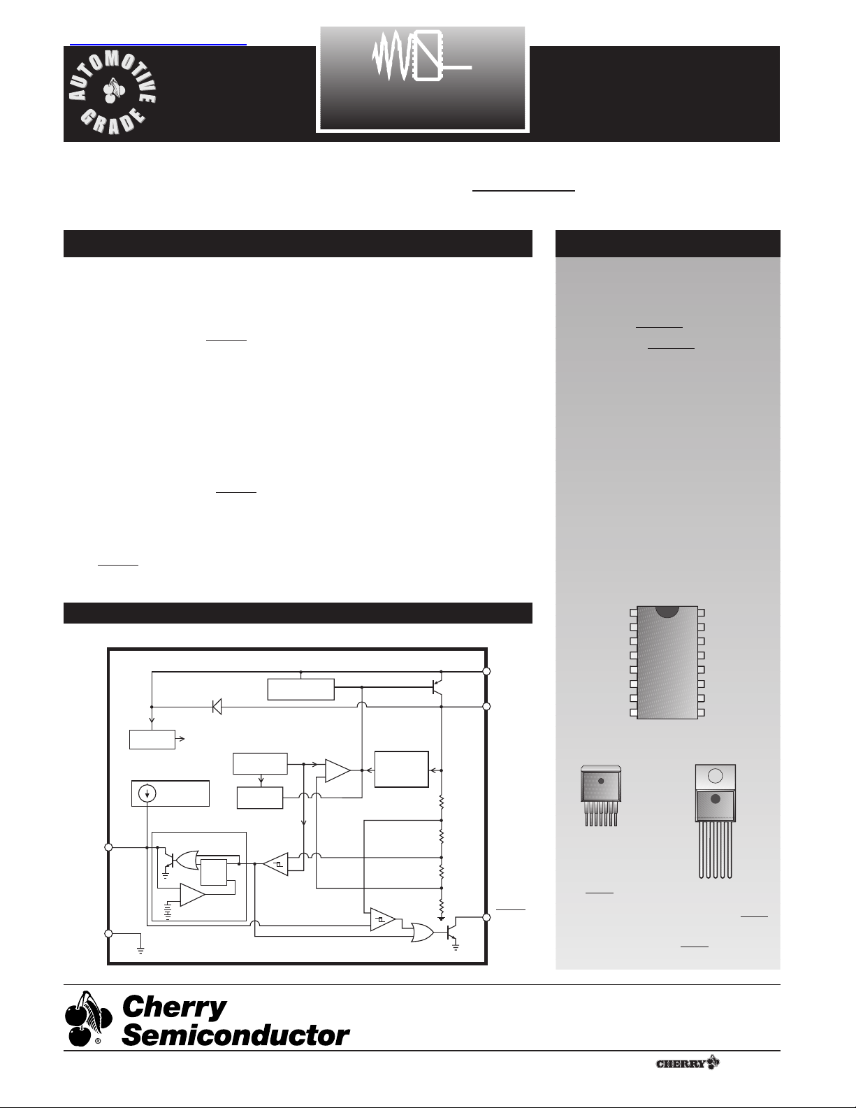
Block Diagram
CS8126-1
1V
IN
2V
OUT
3 Gnd
4 Delay
5 RESET
CS8126-2
1V
IN
2 RESET
3 Gnd
4 Delay
5V
OUT
16 Lead SOIC Wide
V
IN
V
OUT
Delay
РРРРРР
RESET
V
OUT(SENSE)
NC
NC
Gnd
NC
NC
NC
NC
NC
NC
NC
NC
A Company
¨
Rev. 5/4/99
1
1V
IN
2V
OUT
3V
OUT(SENSE)
4 Gnd
5 Delay
6 RESET
7NC
Cherry Semiconductor Corporation
2000 South County Trail, East Greenwich, RI 02818
Tel: (401)885-3600 Fax: (401)885-5786
Email: info@cherry-semi.com
Web Site: www.cherry-semi.com
查询CS8126-1YT5供应商
Over Voltage
Shutdown
V
IN
V
OUT
1
Delay
Gnd
Regulator
Pre-
Charge
Current
Generator
V
Regulated Supply
for Circuit Bias
Latching
Discharge
QRS
-
+
Discharge
Bandgap
Reference
Thermal
Shutdown
Comparator
Reset
Error
Amp
-
+
-
+
Anti-Saturation
and
Current Limit
Delay
Comparator
+
-
RESET
Page 2
2
PARAMETER TEST CONDITIONS MIN TYP MAX UNIT
Electrical Characteristics: TA= -40ûC to +125ûC, TJ= -40ûC to +150ûC, VIN= 6 to 26V, IO=5 to 500mA,
R
RESET
= 4.7k½ to V
CC,
unless otherwise noted.
Absolute Maximum Ratings
Power Dissipation.............................................................................................................................................Internally Limited
Peak Transient Voltage (46V Load Dump) .................................................................................................................-50V, 60V
Output Current .................................................................................................................................................Internally Limited
ESD Susceptibility (Human Body Model)..............................................................................................................................4kV
Junction Temperature.............................................................................................................................................-40¡C to 150¡C
Storage Temperature...............................................................................................................................................-55¡C to 150¡C
Lead Temperature Soldering Wave Solder (through hole styles only) ..........................................10 sec. max, 260¡C peak
Reflow (SMD styles only) ..........................................60 sec. max above 183¡C, 230¡C peak
■ Output Stage (V
OUT
)
Output Voltage 4.85 5.00 5.15 V
Dropout Voltage I
OUT
= 500mA 0.35 0.60 V
Supply Current I
OUT
² 10mA 2 7 mA
I
OUT
² 100mA 6 12
I
OUT
² 500mA 55 100
Line Regulation VIN= 6 to 26V, I
OUT
= 50mA 5 50 mV
Load Regulation I
OUT
= 50 to 500mA, VIN= 14V 10 50 mV
Ripple Rejection f = 120Hz, VIN= 7 to 17V, 54 75 dB
I
OUT
= 250mA
Current Limit 0.75 1.20 A
Overvoltage Shutdown 32 40 V
Maximum Line Transient V
OUT
² 5.5V 95 V
Reverse Polarity Input V
OUT
³ -0.6V, 10½ Load -15 -30 V
Voltage DC
Reverse Polarity Input 1% Duty Cycle, T < 100ms, -80 V
Voltage Transient 10½ Load
Thermal Shutdown Guaranteed by Design 150 180 210 ¡C
■ and Delay Functions
Delay Charge Current V
Delay
= 2V 5 10 15 µA
Threshold V
OUT
Increasing, V
RT(ON)
4.65 4.90 V
OUT
- 0.01 V
V
OUT
Decreasing, V
RT(OFF)
4.50 4.70 V
OUT
- 0.15 V
Hysteresis V
RH
= V
RT(ON)
- V
RT(OFF)
150 200 250 mV
Delay Threshold Charge, V
DC(HI)
3.25 3.50 3.75 V
Discharge, V
DC(LO)
2.85 3.10 3.35 V
Delay Hysteresis 200 400 800 mV
Output Voltage Low 1V < V
OUT
< V
RTL
, 3k½ to V
OUT
0.1 0.4 V
Output Leakage V
OUT
> V
RT(ON)
010µA
Current
Delay Capacitor Discharge Latched ÒONÓ, 0.2 0.5 V
Discharge Voltage V
OUT
> V
RT
Delay Time C
Delay
= 0.1µF* (Note 1) 16 32 48 ms
Delay Time = = C
Delay
x 3.2 x 10⁵(typ)
Note 1: assumes ideal capacitor
C
Delay
´ V
Delay
Threshold Charge
I
Charge
RESET
RESET
RESET
RESET
RESET
CS8126, -1, -2
Page 3
3
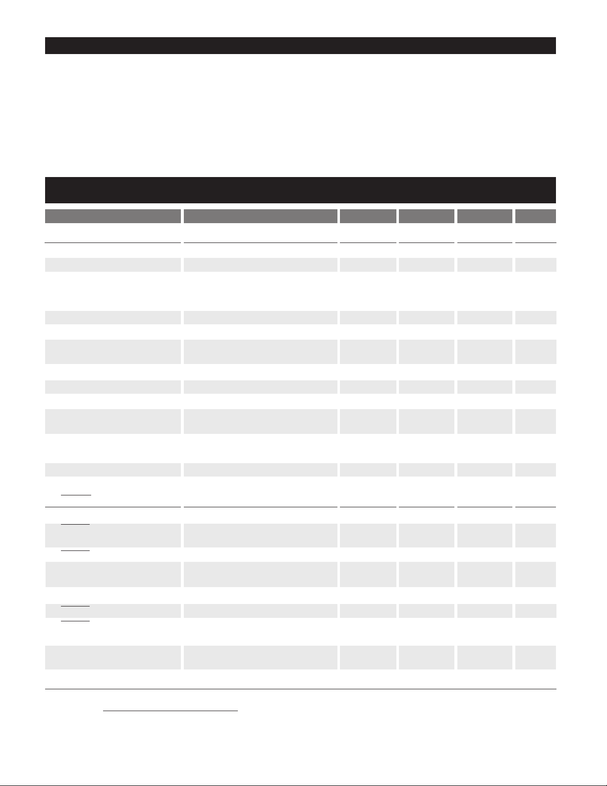
Typical Performance Characteristics
V
OUT
vs VINover Temperature
ICQvs. VINover R
LOAD
ICQvs. VINover Temperature
V
OUT
vs. VINover R
LOAD
Package Lead Description
PACKAGE LEAD # LEAD SYMBOL FUNCTION
CS8126, -1, -2
5 Lead TO-220 7Lead 16 Lead
8126-1 8126-2 D2PAK SOIC Wide
11 1 1 V
IN
Unregulated supply voltage to IC.
25 2 16 V
OUT
Regulated 5V output.
3 3 4 11 Gnd Ground connection.
4 4 5 8 Delay Timing capacitor for function.
5 2 6 6 CMOS/TTL compatible output lead. goes low
after detection of any error in the regulated output or
during power up.
314V
OUT(SENSE)
Remote sensing of output voltage.
7 2, 3, 4, 5, 7, 9, NC No Connection.
10, 12, 13, 15
RESETRESET
RESET
55.0
50.0
45.0
40.0
35.0
30.0
25.0
ICQ (mA)
20.0
15.0
10.0
5.0
0.0
5.5
5.0
4.5
4.0
3.5
3.0
(V)
2.5
OUT
V
2.0
1.5
1.0
0.5
0.0
125ûC
0.0
1.0 2.0 3.0 4.0 5.0 6.0 7.0 8.0 9.0 10.0
125ûC
25ûC
0.0
1.0 2.0 3.0 4.0 5.0 6.0 7.0 8.0 9.0 10.0
R
25ûC
-40ûC
R
-40ûC
LOAD
VIN (V)
LOAD
VIN (V)
= 25W
= 25W
120.0
110.0
100.0
90.0
80.0
70.0
60.0
50.0
ICQ (mA)
40.0
30.0
20.0
10.0
0.0
5.5
5.0
4.5
4.0
3.5
3.0
(V)
2.5
OUT
V
2.0
1.5
1.0
0.5
0.0
0.0
1.0 2.0 3.0 4.0 5.0 6.0 7.0 8.0 9.0 10.0
Rload =
NO LOAD
Rload = 10
1.0 2.0 3.0 4.0 5.0 6.0 7.0 8.0 9.0 10.0
0.0
Room Temp.
VIN (V)
Room Temp.
Rload = 6.67
VIN (V)
R
load
R
= 25
load
R
= NO LOAD
load
R
load
= 10
= 6.67
Page 4

4
0
0
Quiescent Current (mA)
Output Current (mA)
10
20
30
40
50
60
70
80
90
100
100 200 300 400 500 600 700 800
VIN = 14V
125ûC
25ûC
-40ûC
Ripple Rejection
Quiescent Current vs. Output Current over Temperature
Dropout Voltage vs. Output Current over Temperature
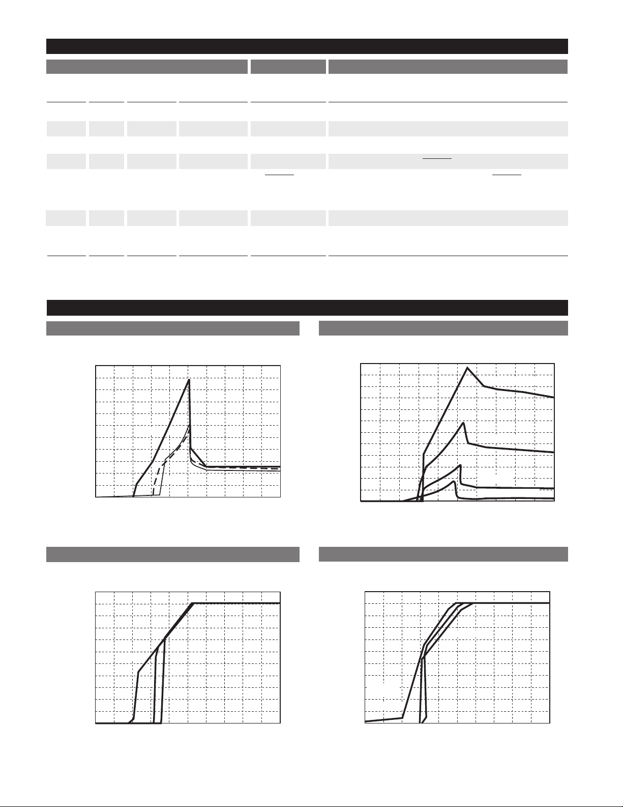
Typical Performance Characteristics: continued
-100
0
Line Regulation (mV)
Output Current (mA)
-80
-60
-40
-20
0
20
40
60
80
100
100 200 300 400 500 600 700 800
VIN 6-26V
TEMP = 25ûC
TEMP = 40ûC
TEMP = 125ûC
-14
0
Load Regulation (mV)
Output Current (mA)
-12
-10
-8
-6
-4
-2
0
2
4
6
100 200 300 400 500 600 700 800
TEMP = 25ûC
TEMP = 125ûC
VIN = 14V
TEMP = -40ûC
Load Regulation vs. Output Current over Temperature
Line Regulation vs. Output Current over Temperature
10
0
ESR (ohms)
Output Current (mA)
10
1
10
2
10
3
10
1
10
2
10
3
10
-4
10
0
10
-1
10
-2
10
-3
C
OUT
= 68mF
C
OUT
= 47mF
C
OUT
= 47/68mF
Stable Region
Output Capacitor ESR
CS8126, -1, -2
900
800
700
600
500
400
300
Dropout Voltage (mV)
200
100
0
0
100 200 300 400 500 600 700 800
125ûC
-40ûC
Output Current (mA)
25ûC
90
80
70
60
50
40
Rejection (dB)
30
20
10
0
I
= 250mA
0
10
10110210310410510610710
OUT
C
= 10mF, ESR = 1W
OUT
C
OUT
Freq. (Hz)
C
= 10mF, ESR = 1 & 0.1mF,
OUT
ESR = 0
= 10mF, ESR = 10W
8
Page 5

5
The CS8126 function, has hysteresis on both the
Reset and Delay comparators, a latching Delay capacitor
discharge circuit, and operates down to 1V.
The circuit output is an open collector type with
ON and OFF parameters as specified. The output
NPN transistor is controlled by the two circuits described
(see Block Diagram).
Low Voltage Inhibit Circuit
This circuit monitors output voltage, and when the output
voltage falls below V
RT(OFF)
, causes the output transistor to be in the ON (saturation) state. When the output
voltage rises above V
RT(ON)
, this circuit permits the
output transistor to go into the OFF state if allowed by
the Delay circuit.
RESET Delay Circuit
This circuit provides a programmable (by external capacitor) delay on the output lead. The Delay lead provides source current to the external delay capacitor only
when the "Low Voltage Inhibit" circuit indicates that output voltage is above V
RT(ON)
. Otherwise, the Delay lead
sinks current to ground (used to discharge the delay
capacitor). The discharge current is latched ON when the
output voltage falls below V
RT(OFF)
. The Delay capacitor is
fully discharged anytime the output voltage falls out of
regulation, even for a short period of time. This feature
ensures a controlled pulse is generated following
detection of an error condition. The circuit allows
the output transistor to go to the OFF (open) state
only when the voltage on the Delay lead is higher than
V
DC(H1)
.
The Delay time for the function is calculated from
the formula:
Delay time =
Delay time = C
Delay
´ 3.2 ´ 10
5
If C
Delay
= 0.1µF, Delay time (ms) = 32ms ± 50%: i.e. 16ms
to 48ms. The tolerance of the capacitor must be taken into
account to calculate the total variation in the delay time.
C
Delay
´ V
Delay
Threshold
I
Charge
RESET
RESET
RESET
RESET
RESET
RESET
RESET
RESET
RESET
RESET
RESET Circuit Waveform
V
RH
V
OUT
V
RT(ON)
V
RT(OFF)
V
RL
Delay
V
DC(HI)
V
DC(LO)
V
DH
t
Delay
V
DIS
(3)
(1)
(2)
(2)
RESET
(1) = No Delay Capacitor
(2) = With Delay Capacitor
(3) = Max: RESET Voltage (1.0V)
Circuit Description
CS8126, -1, -2
Page 6

6
Application Diagram
Application Notes
C1*
100nF
V
IN
Delay
Gnd
RESET
V
OUT
CS8126
C2**
10mF to 100mF
R
RST
4.7kW
Delay
0.1mF
The output or compensation capacitor helps determine
three main characteristics of a linear regulator: start-up
delay, load transient response and loop stability.
The capacitor value and type should be based on cost,
availability, size and temperature constraints. A tantalum
or aluminum electrolytic capacitor is best, since a film or
ceramic capacitor with almost zero ESR, can cause instability. The aluminum electrolytic capacitor is the least
expensive solution, but, if the circuit operates at low temperatures (-25¡C to -40¡C), both the value and ESR of the
capacitor will vary considerably. The capacitor manufacturers data sheet usually provides this information.
The value for the output capacitor C2shown in the test
and applications circuit should work for most applications, however it is not necessarily the optimized solution.
To determine an acceptable value for C2for a particular
application, start with a tantalum capacitor of the recommended value and work towards a less expensive alternative part.
Step 1: Place the completed circuit with a tantalum capacitor of the recommended value in an environmental chamber at the lowest specified operating temperature and
monitor the outputs with an oscilloscope. A decade box
connected in series with the capacitor will simulate the
higher ESR of an aluminum capacitor. Leave the decade
box outside the chamber, the small resistance added by
the longer leads is negligible.
Step 2: With the input voltage at its maximum value,
increase the load current slowly from zero to full load
while observing the output for any oscillations. If no oscillations are observed, the capacitor is large enough to
ensure a stable design under steady state conditions.
Step 3: Increase the ESR of the capacitor from zero using
the decade box and vary the load current until oscillations
appear. Record the values of load current and ESR that
cause the greatest oscillation. This represents the worst
case load conditions for the regulator at low temperature.
Step 4: Maintain the worst case load conditions set in step
3 and vary the input voltage until the oscillations increase.
This point represents the worst case input voltage conditions.
Step 5: If the capacitor is adequate, repeat steps 3 and 4
with the next smaller valued capacitor. A smaller capacitor will usually cost less and occupy less board space. If
the output oscillates within the range of expected operating conditions, repeat steps 3 and 4 with the next larger
standard capacitor value.
Step 6: Test the load transient response by switching in
various loads at several frequencies to simulate its real
working environment. Vary the ESR to reduce ringing.
Step 7: Remove the unit from the environmental chamber
and heat the IC with a heat gun. Vary the load current as
instructed in step 5 to test for any oscillations.
Once the minimum capacitor value with the maximum
ESR is found, a safety factor should be added to allow for
the tolerance of the capacitor and any variations in regulator performance. Most good quality aluminum electrolytic
capacitors have a tolerance of +/- 20% so the minimum
value found should be increased by at least 50% to allow
for this tolerance plus the variation which will occur at
low temperatures. The ESR of the capacitor should be less
than 50% of the maximum allowable ESR found in step 3
above.
The maximum power dissipation for a single output regulator (Figure 1) is:
P
D(max)
= {V
IN(max)
- V
OUT(min)}IOUT(max)
+ V
IN(max)IQ
(1)
where:
V
IN(max)
is the maximum input voltage,
V
OUT(min)
is the minimum output voltage,
I
OUT(max)
is the maximum output current for the applica-
tion, and
IQis the quiescent current the regulator consumes at
I
OUT(max)
.
Stability Considerations
Calculating Power Dissipation
in a Single Output Linear Regulator
C1* is required if the regulator is far from the power source filter.
C
2
** is required for stability
CS8126, -1, -2
Page 7

7
Application Notes: continued
Once the value of P
D(max)
is known, the maximum permis-
sible value of R
QJA
can be calculated:
R
QJA
=
(2)
The value of R
QJA
can then be compared with those in
the package section of the data sheet. Those packages with
R
QJA
's less than the calculated value in equation 2 will keep
the die temperature below 150¡C.
In some cases, none of the packages will be sufficient to
dissipate the heat generated by the IC, and an external
heatsink will be required.
A heat sink effectively increases the surface area of the
package to improve the flow of heat away from the IC and
into the surrounding air.
Each material in the heat flow path between the IC and the
outside environment will have a thermal resistance. Like
series electrical resistances, these resistances are summed
to determine the value of R
QJA
.
R
QJA
= R
QJC
+ R
QCS
+ R
QSA
(3)
where:
R
QJC
= the junctionÐtoÐcase thermal resistance,
R
QCS
= the caseÐtoÐheatsink thermal resistance, and
R
QSA
= the heatsinkÐtoÐambient thermal resistance.
R
QJC
appears in the package section of the data sheet. Like
R
QJA
, it is a function of package type. R
QCS
and R
QSA
are
functions of the package type, heatsink and the interface
between them. These values appear in heat sink data
sheets of heat sink manufacturers.
150¡C - T
A
P
D
Heat Sinks
Figure 1. Single output regulator with key performance parameters
labeled.
CS8126, -1, -2
I
V
IN
IN
Regulator
Control
Features
}
Smart
I
Q
I
OUT
V
OUT
Page 8

5 Lead 7 Lead 16 Lead
Thermal Data TO-220 D2PAK SOIC Wide
R
QJC
typ 2.1 2.1 23 ûC/W
R
QJA
typ 50 10-50* 105 ûC/W
*Depending on thermal properties of substrate. R
QJA
= R
QJC
+ R
QCA
.
D
Lead Count Metric English
Max Min Max Min
16 Lead SO Wide 10.50 10.10 .413 .398
8
CS8126
Package Specification
PACKAGE THERMAL DATA
PACKAGE DIMENSIONS IN mm (INCHES)
Surface Mount Wide Body (DW); 300 mil wide
1.27 (.050) BSC
7.60 (.299)
7.40 (.291)
10.65 (.419)
10.00 (.394)
D
0.32 (.013)
0.23 (.009)
1.27 (.050)
0.40 (.016)
REF: JEDEC MS-013
2.49 (.098)
2.24 (.088)
0.51 (.020)
0.33 (.013)
2.65 (.104)
2.35 (.093)
0.30 (.012)
0.10 (.004)
5 Lead TO-220 (T) Straight
2.87 (.113)
2.62 (.103)
6.93(.273)
6.68(.263)
9.78 (.385)
10.54 (.415)
1.02(.040)
0.63(.025)
1.83(.072)
1.57(.062)
0.56 (.022)
0.36 (.014)
2.92 (.115)
2.29 (.090)
1.40 (.055)
1.14 (.045)
4.83 (.190)
4.06 (.160)
6.55 (.258)
5.94 (.234)
14.22 (.560)
13.72 (.540)
1.02 (.040)
0.76 (.030)
3.71 (.146)
3.96 (.156)
14.99 (.590)
14.22 (.560)
5 Lead TO-220 (THA) Horizontal
0.81(.032)
1.70 (.067)
6.81(.268)
1.40 (.055)
1.14 (.045)
5.84 (.230)
6.60 (.260)
6.83 (.269)
0.56 (.022)
0.36 (.014)
10.54 (.415)
9.78 (.385)
6.55 (.258)
5.94 (.234)
3.96 (.156)
3.71 (.146)
1.68
(.066)
TYP
14.99 (.590)
14.22 (.560)
2.77 (.109)
2.29 (.090)
2.92 (.115)
4.83 (.190)
4.06 (.160)
2.87 (.113)
2.62 (.103)
5 Lead TO-220 (TVA) Vertical
1.68
(.066) typ
1.70 (.067)
7.51 (.296)
1.78 (.070)
4.34 (.171)
0.56 (.022)
0.36 (.014)
1.40 (.055)
1.14 (.045)
4.83 (.190)
4.06 (.160)
14.99 (.590)
14.22 (.560)
2.92 (.115)
2.29 (.090)
.94 (.037)
.69 (.027)
8.64 (.340)
7.87 (.310)
6.80 (.268)
10.54 (.415)
9.78 (.385)
2.87 (.113)
2.62 (.103)
6.55 (.258)
5.94 (.234)
3.96 (.156)
3.71 (.146)
Page 9

9
Part Number Description
CS8126-1YT5 5 Lead TO-220 Straight
CS8126-1YTVA5 5 Lead TO-220 Vertical
CS8126-1YTHA5 5 Lead TO-220 Horizontal
CS8126-2GT5 5 Lead TO-220 Straight
CS8126-2GTVA5 5 Lead TO-220 Vertical
CS8126-2GTHA5 5 Lead TO-220 Horizontal
CS8126-1YTHE5 5 Lead TO-220 Surface Mount
CS8126-1YTHER5 5 Lead TO-220 Surface Mount
(tape & reel)
CS8126YDPS7 7 Lead D2PAK Short-Leaded
CS8126YDPSR7 7 Lead D2PAK Short-Leaded
(tape & reel)
CS8126YDW16 16 Lead SOIC Wide
CS8126YDWR16 16 Lead SOIC Wide (tape & reel)
Rev. 5/4/99
Ordering Information
© 1999 Cherry Semiconductor Corporation
Cherry Semiconductor Corporation reserves the
right to make changes to the specifications without
notice. Please contact Cherry Semiconductor
Corporation for the latest available information.
Package Specification: continued
CS8126
PACKAGE DIMENSIONS IN mm (INCHES)
5 Lead TO-220 (THE) SMD
10.3 (.405)
10.0 (.395)
3.96 (.156)
3.71 (.146)
2.87 (.113)
2.61 (.103)
14.6 (.575)
8.40 (.331)
.914 (.036)
.711 (.028)
1.70 (.067)
6.80 (.268)
4.44 (.175)
.254 (.010)
.000 (.000)
B
.102 (.004) MAX
A
1.40 (.055)
1.14 (.045)
5° (5 Places)
14.0 (.550)
2.66 (.105)
2.56 (.101)
2.03 (.080)
.254 (.010) REF
Notes:
1.Dimensions exclusive of
mold flash and metal burrs.
2.Footpad length measured from
lead tip with ref. to datum .
3.Coplanarity .004² max.
Reference plane standoff
height .000Ð.010².
B
A
7 Lead D2PAK (DPS)* Short-Leaded
1.98 (.078)
1.47 (.058)
14.71 (.579)
13.69 (.539)
4.57 (.180)
4.31 (.170)
1.40 (.055)
1.14 (.045)
2.79 (.110)
2.54 (.100)
TERMINAL 8
7.75 (.305)
REF
6.50 (.256) REF
10.31 (.406)
10.05 (.396)
1.27 (.050)
REF
1.68 (.066)
1.40 (.055)
.254 (.010)
REF
0.91 (.036)
0.66 (.026)
8.53 (.336)
8.28 (.326)
0.10 (.004)
0.00 (.000)
*CHERRY SEMICONDUCTOR SHORT-LEADED FOOTPRINT
 Loading...