

Page 1
The CS8122 is a precision 5V linear regulator capable of sourcing in excess of
750mA. The Õs delay time is
externally programmed using a discrete
RC network. During power up, or when
the output goes out of regulation, the
lead remains in the low state
for the duration of the delay. This function is independent of the input voltage
and will function correctly as long as
the output voltage remains at or above
1V. Hysteresis is included in the Delay
and the comparators to
improve noise immunity. A latching
discharge circuit is used to discharge
the delay capacitor when it is triggered
by a brief fault condition.
The regulator is protected against a
variety of fault conditions: i.e. reverse
battery, overvoltage, short circuit and
thermal runaway conditions. The regulator is protected against voltage transients ranging from -50V to +40V. Short
circuit current is limited to 1.2A (typ).
The CS8122 is an improved replacement
for the CS8126 and features a tighter tolerance on its output voltage (2% vs 4%).
The CS8122 is packaged in a 5 lead
TOÐ220 with copper tab. The copper tab
can be connected to a heat sink if
necessary.
RESET
RESET
RESET
1
2% 5V, 750mA Low Dropout Linear
Regulator with Delayed RESET
Features
■ 5V +/- 2% Regulated
Output
■ Low Dropout Voltage
(0.6V @ 0.5A)
■ 750mA Output Current
Capability
■ Externally Programmed
Delay
■ Fault Protection
Reverse Battery
60V Load Dump
-50V Reverse Transient
Short Circuit
Thermal Shutdown
RESET
Package Options
5 Lead TO-220
CS8122
Description
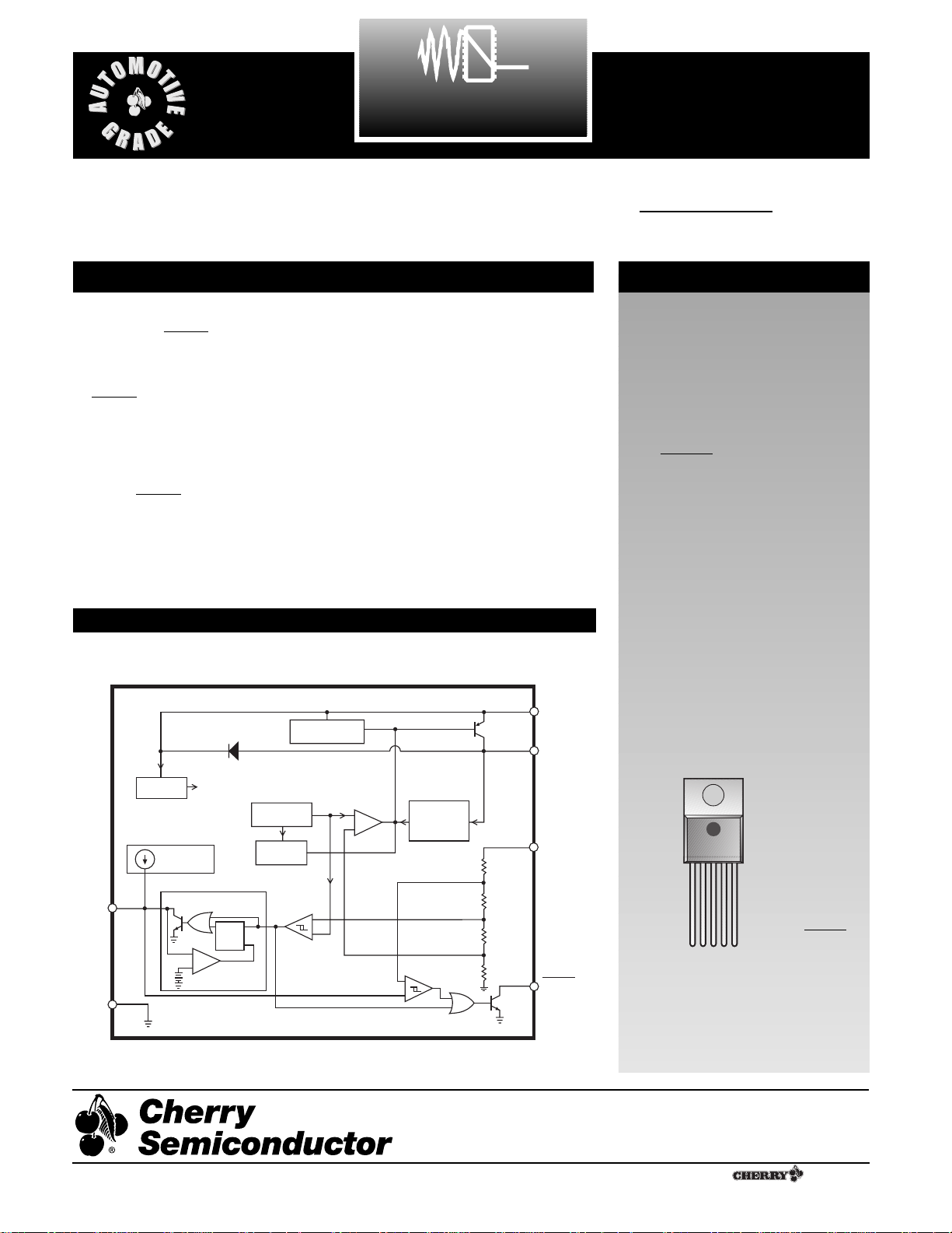
Block Diagram
CS8122
1V
IN
2V
OUT
3 Gnd
4 Delay
5 RESET
1
A Company
¨
Rev. 2/5/99
Cherry Semiconductor Corporation
2000 South County Trail, East Greenwich, RI 02818
Tel: (401)885-3600 Fax: (401)885-5786
Email: info@cherry-semi.com
Web Site: www.cherry-semi.com
Charge
Current
Generator
Regulated Supply
for Circuit Bias
Bandgap
Reference
Thermal
Shutdown
Pre-
Regulator
Over Voltage
Shutdown
Error Amplifier
-
+
Anti-Saturation
and
Current Limit
V
IN
V
OUT
V
OUT
SENSE
Delay
Gnd
Latching Discharge
QRS
-
+
VDISC
-
+
Delay Comparator
+
-
RESET
Page 2
2
Electrical Characteristics: -40ûC ² TA ² +125ûC, -40ûC ² TJ ² +150ûC, 6V ² V
IN
² 26V, 5mA ² I
OUT
² 500mA,
R = 4.7k½ to VCCunless otherwise noted*
RESET
PARAMETER TEST CONDITIONS MIN TYP MAX UNIT
Absolute Maximum Ratings
Input Operating Range..................................................................................................................................................-0.5 to 26V
Power Dissipation.............................................................................................................................................Internally Limited
Transient Input Voltage .................................................................................................................................................-50V, 60V
Output Current .................................................................................................................................................Internally Limited
ESD Susceptibility (Human Body Model)..............................................................................................................................4kV
Junction Temperature.............................................................................................................................................-55¡C to 150¡C
Storage Temperature...............................................................................................................................................-55¡C to 150¡C
Lead Temperature Soldering
Wave Solder (through hole styles only) .....................................................................................10 sec. max, 260¡C peak
CS8122
* To observe safe operating junction temperatures, low duty cycle pulse testing is used in tests where applicable.
Delay Time =
C
Delay
x V
Delay Threshold Charge
= C
Delay
x 3.5 x 10⁵ (typ)
I
Charge
■ Output Stage (V
OUT
)
Output Voltage 4.9 5.0 5.1 V
Dropout Voltage I
OUT
= 500mA 0.35 0.60 V
Supply Current I
OUT
² 10mA 2 7 mA
I
OUT
² 100mA 6 12
I
OUT
² 500mA 55 100
Line Regulation 6V ² V
IN
² 26V, I
OUT
= 50mA 5 50 mV
Load Regulation 50mA ² I
OUT
² 500mA, VIN= 14V 10 50 mV
Ripple Rejection f = 120Hz, VIN= 7 to 17V, 54 75 dB
I
OUT
= 250mA
Current Limit 0.75 1.20 A
Overvoltage Shutdown 32 40 V
Maximum Line Transient V
OUT
² 5.5V 60 95 V
Reverse Polarity Input V
OUT
³ -0.6V, 10½ Load -15 -30 V
Voltage DC
Reverse Polarity Input 1% Duty Cycle, T < 100ms, -50 -80 V
Voltage Transient 10½ Load
Thermal Shutdown Guaranteed by Design 150 180 210 ¡C
■ and Delay Functions
Delay Charge Current V
DELAY
= 2V 5 10 15 µA
Threshold V
OUT
Increasing, V
RT(ON)
4.65 4.90 V
OUT
-0.01 V
V
OUT
Decreasing, V
RT(OFF)
4.50 4.70 V
OUT
-0.16 V
Hysteresis V
RH
= V
RT(ON)
- V
RT(OFF)
150 200 250 mV
Delay Threshold Charge, V
DC(HI)
3.25 3.50 3.75 V
Discharge, V
DC(L)
2.85 3.10 3.35 V
Delay Hysteresis 200 400 800 mV
Output Voltage Low 1V < V
OUT
< V
RT(L)
, 3k½ to V
OUT
0.1 0.4 V
Output Leakage V
OUT
> V
RT(H)
010µA
Current
Delay Capacitor Discharge Latched ÒONÓ, 0.2 0.5 V
Discharge Voltage V
OUT
> V
RT
Delay Time C
DELAY
= 0.1µF 16 32 48 ms
RESET
RESET
RESET
RESET
RESET
Page 3
3
Typical Performance Characteristics
0.0
0.0
Quiescent Current
(mA)
VIN (V)
1.0 2.0 3.0 4.0 5.0 6.0 7.0 8.0 9.0 10.0
5.0
10.0
15.0
20.0
25.0
30.0
35.0
40.0
45.0
50.0
55.0
125ûC
25ûC
-40ûC
R
load
= 25W
0.0
0.0
Quiescent Current
(mA)
VIN (V)
1.0 2.0 3.0 4.0 5.0 6.0 7.0 8.0 9.0 10.0
20.0
40.0
60.0
80.0
100.0
120.0
R
load
= 6.67W
R
load
= 10W
R
load
= 25W
R
load
= NO LOAD
Room Temp.
Output Voltage vs Input Voltage over Temperature
Quiescent Current vs Input Voltage over Load Resistance
Quiescent Current vs Input Voltage over Temperature
0.0
0.0
V
OUT
(V)
VIN (V)
1.0 2.0 3.0 4.0 5.0 6.0 7.0 8.0 9.0 10.0
0.5
1.0
1.5
2.0
2.5
3.0
3.5
4.0
4.5
5.0
5.5
R
load
=
NO LOAD
R
load
= 6.67W
R
load
= 10W
Room Temp.
V
OUT
vs. VINover R
LOAD
Package Lead Description
PACKAGE LEAD # LEAD SYMBOL FUNCTION
CS8122
R
load
=25½
5Lead TO-220
1V
IN
Unregulated supply voltage to IC.
2V
OUT
Regulated 5V output.
3 Gnd Ground connection.
4 Delay Timing capacitor for function.
5 CMOS/TTL compatible output lead. goes low whenev-
er V
OUT
drops below 6% of it's regulated value.
RESET
RESET
RESET
R
= 25W
5.5
load
5.0
4.5
4.0
3.5
3.0
2.5
2.0
1.5
1.0
0.5
0.0
-40ûC
VIN (V)
125ûC
25ûC
0.0
1.0 2.0 3.0 4.0 5.0 6.0 7.0 8.0 9.0 10.0
(V)
OUT
V
Page 4

4
0
0
QUIESCENT CURRENT (mA)
OUTPUT CURRENT (mA)
10
20
30
40
50
60
70
80
90
100
100 200 300 400 500 600 700 800
VIN = 14V
125ûC
25ûC
-40ûC
0
10
0
REJECTION (dB)
FREQUENCY (Hz)
10110210310410510610710
8
10
20
30
40
50
60
70
80
90
I
OUT
= 250mA
C
OUT
= 10mF, ESR = 10W
C
OUT
= 10mF, ESR = 1W
C
OUT
= 10mF, ESR = 1 & 0.1mF,
ESR = 0
Ripple Rejection
Quiescent Current vs. Output CurrentDropout Voltage vs. Output Current
Typical Performance Characteristics: continued
-100
0
LINE REGULATION (mV)
OUTPUT CURRENT (mA)
-80
-60
-40
-20
0
20
40
60
80
100
100 200 300 400 500 600 700 800
VIN 6-26V
TEMP = 25ûC
TEMP = - 40ûC
TEMP = 125ûC
Load Regulation vs. Output Current
Line Regulation vs. Output Current
10
0
ESR (ohms)
Output Current (mA)
10
1
10
2
10
3
10
1
10
2
10
3
10
-4
10
0
10
-1
10
-2
10
-3
CO= 68mF
CO= 47mF
CO= 47/68mF
Stable Region
Output Capacitor ESR
CS8122
900
800
700
600
500
400
300
200
DROPOUT VOLTAGE (mV)
100
0
0
100 200 300 400 500 600 700 800
OUTPUT CURRENT (mA)
125ûC
-40ûC
25ûC
6
4
2
TEMP = -40ûC
0
-2
-4
-6
-8
LOAD REGULATION (mV)
-10
VIN = 14V
TEMP = 125ûC
-12
-14
100 200 300 400 500 600 700 800
0
OUTPUT CURRENT (mA)
TEMP = 25ûC
Page 5

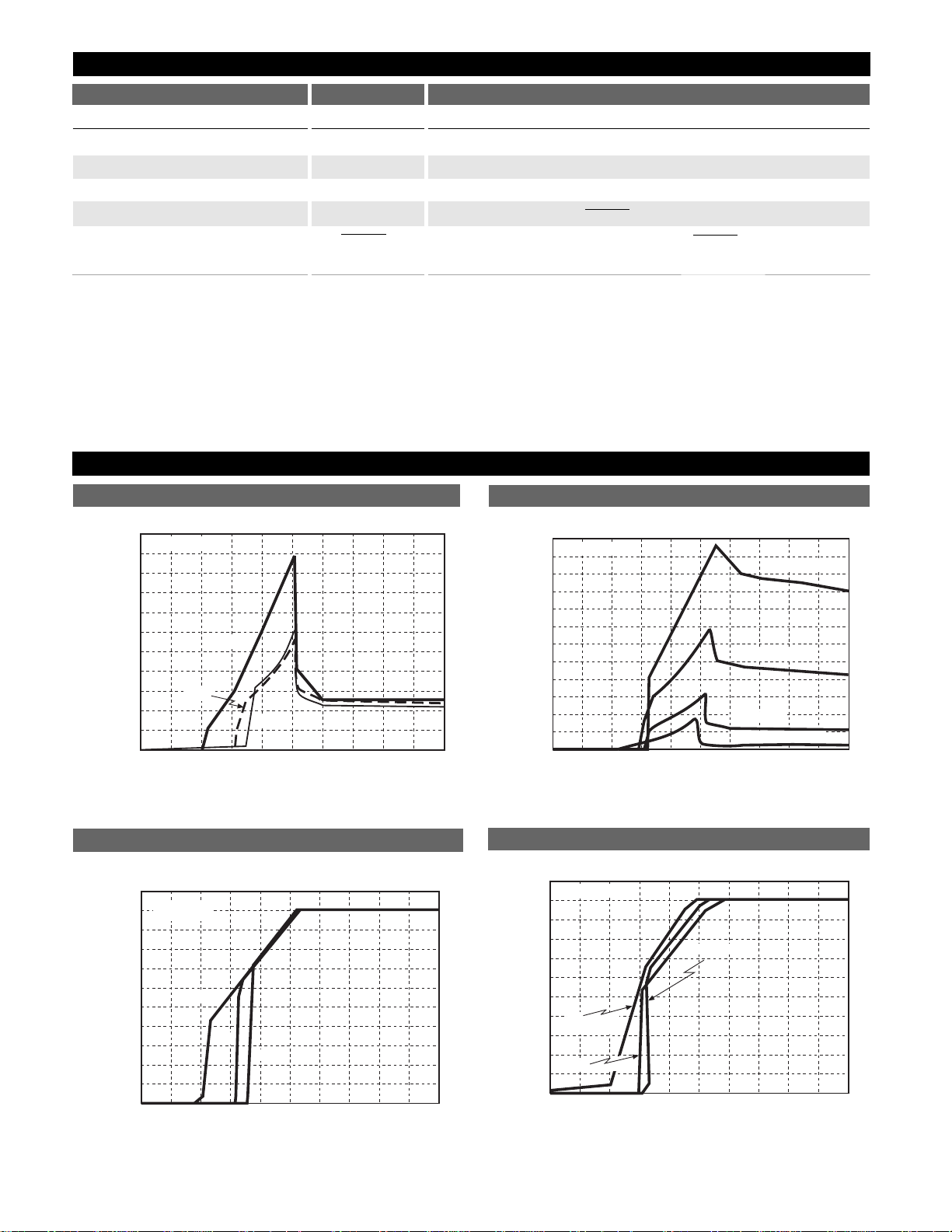
The CS8122 function, has hysteresis on both the
reset and delay comparators, a latching Delay capacitor
discharge circuit, and operates down to 1V.
The circuit output is an open collector type with
ON and OFF parameters as specified. The output
NPN transistor is controlled by the two circuits described
(see Block Diagram).
The Low Voltage Inhibit Circuit monitors output voltage,
and when output voltage is below the specified minimum,
causes the output transistor to be in the ON (saturation) state. When the output voltage is above the specified level, this circuit permits the output transistor
to go into the OFF state if allowed by the Delay circuit.
The Reset Delay Circuit provides a programmable (by
external capacitor) delay on the output lead. The
Delay lead provides source current to the external delay
capacitor only when the Low Voltage Inhibit circuit indicates that output voltage is above V
RT(ON)
. Otherwise, the
Delay lead sinks current to ground (used to discharge the
delay capacitor). The discharge current is latched ON
when the output voltage is below V
RT(OFF)
. The Delay
capacitor is fully discharged anytime the output voltage
falls out of regulation, even for a short period of time. This
feature ensures that a controlled pulse is generated
following detection of an error condition. The circuit
allows the output transistor to go to the OFF (open)
state only when the voltage on the Delay lead is higher
than V
DC(HI)
.
RESET
RESET
RESET
Reset Delay Circuit
RESET
RESET
RESET
Low Voltage Inhibit Circuit
RESET
RESET
RESET
5
V
RH
V
OUT
V
RT(ON)
V
RT(OFF)
V
RL
Delay
V
DC(HI)
V
DC(LO)
V
DH
t
Delay
V
DIS
(3)
(1)
(2)
(2)
RESET
(1) = No Delay Capacitor
(2) = With Delay Capacitor
(3) = Max: RESET Voltage (1.0V)
RESET Circuit Waveform
Circuit Description
Test Circuit
CIN*
100nF
V
IN
Delay
Gnd
RESET
V
OUT
CS8122
C
OUT
**
10mF
R
RST
4.7kW
C
Delay
0.1mF
CS8122
*CINrequired if regulator is far from power source filter.
**C
OUT
required for stability.
Page 6

6
CS8122
Application Notes
The output or compensation capacitor helps determine
three main characteristics of a linear regulator: start-up
delay, load transient response and loop stability.
The capacitor value and type should be based on cost,
availability, size and temperature constraints. A tantalum
or aluminum electrolytic capacitor is best, since a film or
ceramic capacitor with almost zero ESR can cause instability. The aluminum electrolytic capacitor is the least expensive solution, but, if the circuit operates at low temperatures (-25¡C to -40¡C), both the value and ESR of the
capacitor will vary considerably. The capacitor manufacturers data sheet usually provides this information.
The value for the output capacitor C
OUT
shown in the test
and applications circuit should work for most applications, however it is not necessarily the optimized solution.
To determine an acceptable value for C
OUT
for a particular
application, start with a tantalum capacitor of the recommended value and work towards a less expensive alternative part.
Step 1: Place the completed circuit with a tantalum capacitor of the recommended value in an environmental chamber at the lowest specified operating temperature and
monitor the outputs with an oscilloscope. A decade box
connected in series with the capacitor will simulate the
higher ESR of an aluminum capacitor. Leave the decade
box outside the chamber, the small resistance added by
the longer leads is negligible.
Step 2: With the input voltage at its maximum value,
increase the load current slowly from zero to full load
while observing the output for any oscillations. If no oscillations are observed, the capacitor is large enough to
ensure a stable design under steady state conditions.
Step 3: Increase the ESR of the capacitor from zero using
the decade box and vary the load current until oscillations
appear. Record the values of load current and ESR that
cause the greatest oscillation. This represents the worst
case load conditions for the regulator at low temperature.
Step 4: Maintain the worst case load conditions set in step
3 and vary the input voltage until the oscillations increase.
This point represents the worst case input voltage conditions.
Step 5: If the capacitor is adequate, repeat steps 3 and 4
with the next smaller valued capacitor. A smaller capacitor will usually cost less and occupy less board space. If
the output oscillates within the range of expected operating conditions, repeat steps 3 and 4 with the next larger
standard capacitor value.
Step 6: Test the load transient response by switching in
various loads at several frequencies to simulate its real
working environment. Vary the ESR to reduce ringing.
Step 7: Remove the unit from the environmental chamber
and heat the IC with a heat gun. Vary the load current as
instructed in step 5 to test for any oscillations.
Once the minimum capacitor value with the maximum
ESR is found, a safety factor should be added to allow for
the tolerance of the capacitor and any variations in regulator performance. Most good quality aluminum electrolytic
capacitors have a tolerance of ± 20% so the minimum
value found should be increased by at least 50% to allow
for this tolerance plus the variation which will occur at
low temperatures. The ESR of the capacitor should be less
than 50% of the maximum allowable ESR found in step 3
above.
The maximum power dissipation for a single output regulator (Figure 1) is:
P
D(max)
={V
IN(max)ÐVOUT(min)
}
I
OUT(max)+VIN(max)IQ
(1)
where
V
IN(max)
is the maximum input voltage,
V
OUT(min)
is the minimum output voltage,
I
OUT(max)
is the maximum output current for the applica-
tion, and
IQis the quiescent current the regulator consumes at
I
OUT(max)
.
Once the value of P
D(max)
is known, the maximum permis-
sible value of R
QJA
can be calculated:
R
QJA
=
(2)
The value of R
QJA
can then be compared with those in
the package section of the data sheet. Those packages
with R
QJA
's less than the calculated value in equation 2
will keep the die temperature below 150¡C.
In some cases, none of the packages will be sufficient to
dissipate the heat generated by the IC, and an external
heatsink will be required.
150¡C - T
A
P
D
Calculating Power Dissipation
in a Single Output Linear Regulator
Stability Considerations
Figure 1: Single output regulator with key performance parameters
labeled.
I
V
IN
IN
Smart
I
OUT
Regulator
Control
Features
}
I
Q
V
OUT
Page 7

7
Application Notes: continued
CS8122
A heat sink effectively increases the surface area of the
package to improve the flow of heat away from the IC and
into the surrounding air.
Each material in the heat flow path between the IC and the
outside environment will have a thermal resistance. Like
series electrical resistances, these resistances are summed
to determine the value of R
QJA
:
R
QJA
= R
QJC
+ R
QCS
+ R
QSA
(3)
where:
R
QJC
= the junctionÐtoÐcase thermal resistance,
R
QCS
= the caseÐtoÐheatsink thermal resistance, and
R
QSA
= the heatsinkÐtoÐambient thermal resistance.
R
QJC
appears in the package section of the data sheet. Like
R
QJA
, it too is a function of package type. R
QCS
and R
QSA
are functions of the package type, heatsink and the interface between them. These values appear in heat sink data
sheets of heat sink manufacturers.
Heat Sinks
Page 8

Part Number Description
CS8122YT5 5 Lead TO-220 Straight
CS8122YTHA5 5 Lead TO-220 Horizontal
CS8122YTVA5 5 Lead TO-220 Vertical
8
Rev. 2/5/99
CS8122
Ordering Information
Thermal Data 5 Lead TO-220
R
Q
JC
typ 2.1 ûC/W
R
Q
JA
typ 50 ûC/W
Package Specification
PACKAGE THERMAL DATA
PACKAGE DIMENSIONS IN mm(INCHES)
© 1999 Cherry Semiconductor Corporation
Cherry Semiconductor Corporation reserves the
right to make changes to the specifications without
notice. Please contact Cherry Semiconductor
Corporation for the latest available information.
5 Lead TO-220 (T) Straight
2.87 (.113)
2.62 (.103)
6.93(.273)
6.68(.263)
9.78 (.385)
10.54 (.415)
1.02(.040)
0.63(.025)
1.83(.072)
1.57(.062)
0.56 (.022)
0.36 (.014)
2.92 (.115)
2.29 (.090)
1.40 (.055)
1.14 (.045)
4.83 (.190)
4.06 (.160)
6.55 (.258)
5.94 (.234)
14.22 (.560)
13.72 (.540)
1.02 (.040)
0.76 (.030)
3.71 (.146)
3.96 (.156)
14.99 (.590)
14.22 (.560)
5 Lead TO-220 (TVA) Vertical
1.68
(.066) typ
1.70 (.067)
7.51 (.296)
1.78 (.070)
4.34 (.171)
0.56 (.022)
0.36 (.014)
1.40 (.055)
1.14 (.045)
4.83 (.190)
4.06 (.160)
14.99 (.590)
14.22 (.560)
2.92 (.115)
2.29 (.090)
.94 (.037)
.69 (.027)
8.64 (.340)
7.87 (.310)
6.80 (.268)
10.54 (.415)
9.78 (.385)
2.87 (.113)
2.62 (.103)
6.55 (.258)
5.94 (.234)
3.96 (.156)
3.71 (.146)
5 Lead TO-220 (THA) Horizontal
0.81(.032)
1.70 (.067)
6.81(.268)
1.40 (.055)
1.14 (.045)
5.84 (.230)
6.60 (.260)
6.83 (.269)
0.56 (.022)
0.36 (.014)
10.54 (.415)
9.78 (.385)
6.55 (.258)
5.94 (.234)
3.96 (.156)
3.71 (.146)
1.68
(.066)
TYP
14.99 (.590)
14.22 (.560)
2.77 (.109)
2.29 (.090)
2.92 (.115)
4.83 (.190)
4.06 (.160)
2.87 (.113)
2.62 (.103)
 Loading...