

Page 1
CS5525
CS5526
16-Bit/20-Bit Multi-Range ADC with 4-Bit Latch
Features
l
Delta-Sigma A/D Converter
- Linearity Error: 0.0015%FS
- Noise Free Resolution: 18-bits
l
Bipolar/Unipolar Input Ranges
- 25 mV, 55 mV, 100 mV, 1 V, 2.5 V and 5 V
l
Chopper Stabilized Instrumentation Amplifier
l
On-Chip Charge Pump Drive Circuitry
l
4-Bit Output Latch
l
Simple three-wire serial interface
- SPI™ and Microwire™ Compatible
- Schmitt Trigger on Serial Clock (SCLK)
l
Programmable Output Word Rates
- 3.76 Hz to 202Hz (XIN = 32.768 kHz)
- 11.47 Hz to 616 Hz (XIN = 100 kHz)
l
Output Settles in One Conversion Cycle
l
Simultaneous 50/60 Hz Noise Rejection
l
System and Self-Calibration with
Read/Write Registers
l
Single +5 V Analog Supply
+3.0 V or +5 V Digital Supply
l
Low Power Mode Consumption: 4 mW
- 1.8 mW in 1 V, 2.5 V, and 5 V Input Ranges
General Description
The 16-bit CS5525 and the 20-bit CS5526 ar e highl y integrated
instrumentation amplifier, a PGA (programmable gain
amplifier), eight digital filters, and self and system calibration circuitry.
The converters are designed to provide their own negative supply which enables their on-chip instrumentation
amplifiers to measure bipolar ground-referenced si gnals
≤
±100 mV. By directly supplying NBV with -2.5 V and
with VA+ at 5 V,
can be measured.
The digital filters provide programmable output update
rates between 3.76 Hz to 202 Hz (XIN = 32.768 kHz).
Output word rates can be increased by appr oximately 3X
by using XIN = 100 kHz. Each filter is designed to settle
to full accuracy for its output update rate in one conversion cycle. The filters with word rates of 15 Hz or less
(XIN = 32.768 kHz) reject both 50 and 6 0 Hz (
interference simultaneously.
Low power, single conversion settling time, programmable output rates, and the ability to handle negative input
signals make these single supply products ideal solutions for isolated and n on-isolated applicati ons.
ORDERING INFORMATION
∆Σ
A/D converters which include an
See page 26.
±2.5 V signals (with respect to groun d)
±3 Hz) line
VA+ AGND VREF+ VREF- VD+DGND
AIN+
AIN-
NBV
A0
A1
A2
A3
Cirrus Logic, Inc.
Crystal Semiconductor Products Division
P.O. Box 17847, Austin, Texas 78760
(512) 445 7222 FAX: (512) 445 7581
http://www.crystal.com
+
X20
-
Latch
Programmable
Gain
Calibration
Memory
CPD
Differential
4th Order
Delta-Sigma
Modulator
Calibration µC
Copyright Cirrus Logic, I nc. 1998
Digital Filter
Clock
Gen.
XIN XOUT
(All Rights Reserv ed)
Calibration
Register
Control
Register
Output
Register
CS
SCLK
SDI
SDO
JAN ‘98
DS202F1
1
Page 2
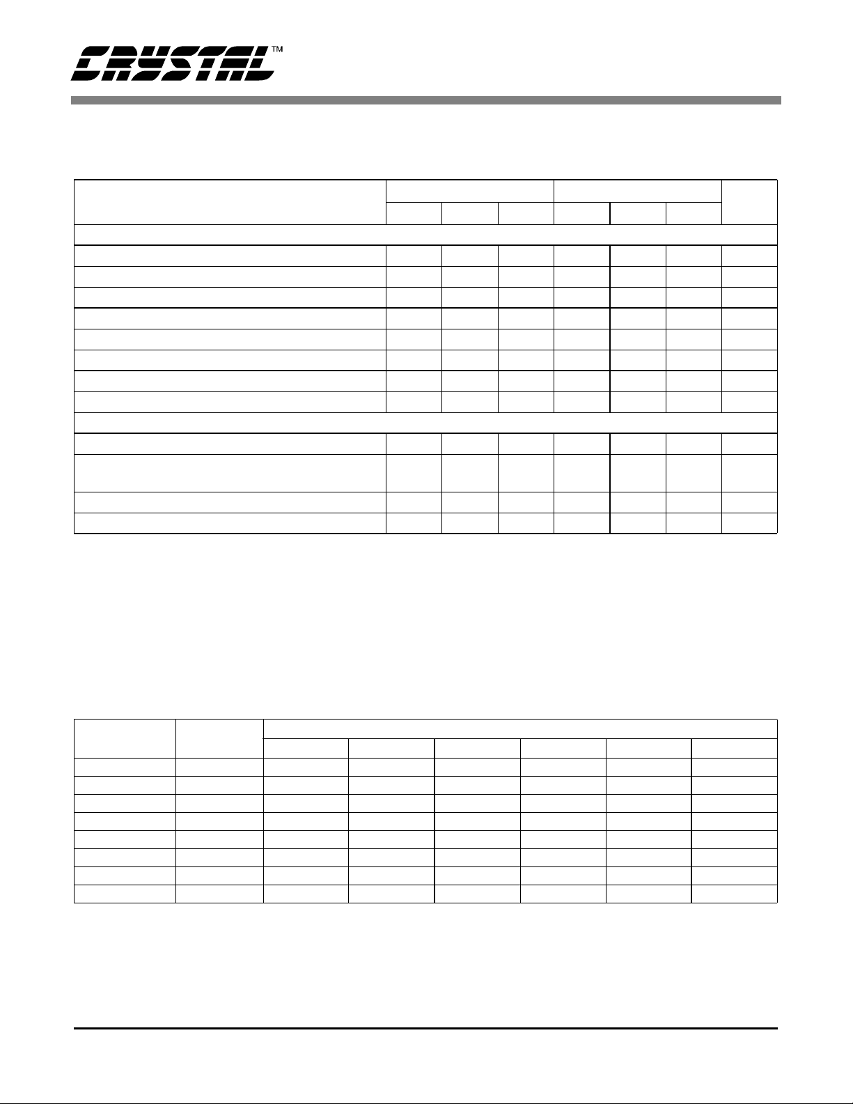
CS5525 CS5526
ANALOG CHARACTERISTICS (T
NBV = -2.1 V, FCLK = 32.768 kHz, OWR (Output Word Rate) = 15 Hz, Bipolar Mode, Input Range = ±100 mV;
See Notes 1 and 2.)
Parameter
= 25 °C; VA+, VD+ = 5 V ±5%; VREF+ = 2.5 V, VREF- = AGND,
A
CS5525 CS5526
Min T yp Max Min Typ Max Unit
Accuracy
Linearity Error No Missing Codes 16 - - 20 - - Bits
Bipolar Offset (Note 3) Unipolar Offset (Note 3) Offset Drift (Notes 3 and 4) - 20 - - 20 - nV/°C
Bipolar Gain Error Unipolar Gain Error Gain Drift (Note 4) - 1 3 - 1 3 ppm/°C
±
0.0015±0.003 -
±
1±2 -
±
2
±
8
±
16
±
4-±32
±
31 -
±
62 -
±
0.0007±0.0015 %FS
±
16 ±32 LSB
±
64 LSB
±
8
±
16
±
31 ppm
±
62 ppm
Voltage Reference Input
Range (VREF+) - (VREF-) 1 2.5 3.0 1 2.5 3.0 V
Common Mode Rejection dc
50, 60 Hz
Input Capacitance - 16 - - 16 - pF
CVF Current (Note 5) - 0.6 - - 0.6 - µA/V
-
-
110
130
-
-
-
-
110
130
-
-
dB
dB
Notes: 1. Applies after system calibration at any temperature within -40 °C ~ +85 °C.
2. Specification s gu aranteed by design, characterization, and/or test.
3. Specification applies to the device only and does not include any effects by external parasitic
thermocouples. LSB = LSB
4. Drift over specified temperature range after calibration at power-up at 25 °C.
5. See the section of the data sheet which discusses input models on page 15.
for the CS5525, and LSB20 for the CS5526.
16
RMS NOISE (Notes 6 and 7)
Output Rate
(Hz)
3.76 3.27 90 nV 90 nV 130 nV 1.0 µV 2.0 µV 4.0 µV
7.51 6.55 110 nV 130 nV 190 nV 1.5 µV 3.0 µV 7 µV
15.0 12.7 170 nV 200 nV 250 nV 2.0 µV 5.0 µV 10 µV
30.1 25.4 250 nV 300 nV 500 nV 4.0 µV 10 µV 15 µV
60.0 50.4 500 nV 1.0 µ V 1.5 µV 15 µV 45 µV 85 µV
123.2 (Note 8) 103.6 2.0 µV 4.0 µ V 8.0 µV 72 µV 190 µV 350 µV
168.9 (Note 8) 141.3 10 µV 20.0 µV 30 µV 340 µV 900 µV 2.0 mV
202.3 (Note 8) 169.2 30 µV 55 µV 105 µV 1.1 mV 2.4 mV 5.3 mV
Notes: 6. Wideband noise aliased int o the baseband. Referred to the input . Typical values shown for 25 °C.
7. For Peak-to-Peak Noise multipl y by 6.6 for all ranges and output rat es.
8. For input ranges <100 mV and output word rates >60 Hz, 32.768 kHz chopping frequency is used.
-3 dB Filter
Frequency
25 mV 55 mV 100 mV 1 V 2.5 V 5 V
Specifications are su bject to change without notice.
Input Range, (Bipolar/Unipolar Mode)
2 DS202F1
Page 3

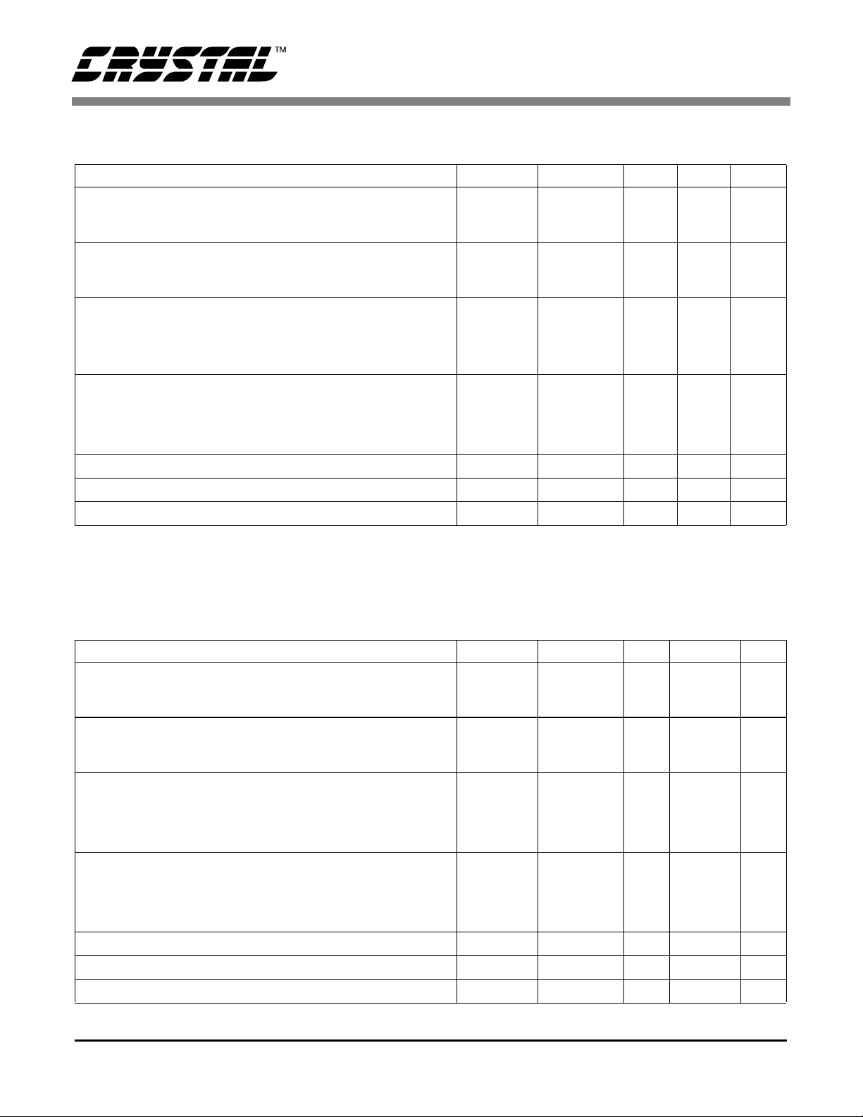
CS5525 CS5526
ANALOG CHARACTERISTICS (Continued)
Parameter Min Typ Max Unit
Analog Input
Common Mode + Signal on AIN+ or AIN- Bipolar/Unipolar Mode
NBV = -1.8 to -2.5 V Range = 25 mV , 55 mV, or 100 mV
Range = 1 V, 2.5 V, or 5 V
NBV = AGND Range = 25 mV, 55 mV, or 100 mV
Range = 1 V, 2.5 V, or 5 V
Common Mode Rejection dc
50, 60 Hz
Input Capacitance - 10 - pF
CVF Current on AIN+ or AIN- (Note 5)
Range = 25 mV, 55 mV, or 100 mV
Range = 1 V, 2.5 V, or 5 V
System Calibration Specifications
Full Scale Calibration Range Bipolar/Unipolar Mode (Note 9)
25 mV
55 mV
100 mV
1 V
2.5 V
5 V
Offset Calibration Range Bipolar/Unipolar Mode
25 mV
55 mV
100 mV (Note 10)
1 V
2.5 V
5 V
Power Supplies
DC Power Supply Currents (Normal Mode) I
Power Consumption Normal Mode (Note 11)
Low Power Mode
St andby
Sleep
Power Supply Rejection dc Positive Supplies
dc NBV
I
NBV
-0.150
NBV
1.85
0.0
-
-
-
-
17.5
38.5
70
0.70
1.75
3.50
-
-
-
-
-
-
A+
I
D+
-
-
-
-
-
-
-
-
-
-
-
-
-
120
120
100
1.2
-
-
-
-
-
-
-
-
-
-
-
-
1.3
15
400
7.5
4.0
1.2
500
95
110
0.950
VA+
2.65
VA+
-
-
300
-
32.5
71.5
105
dB
dB
pA
µA/V
mV
mV
mV
1.30
3.25
VA+
±12.5
±27.5
±50
mV
mV
mV
±0.5
±1.25
±2.50
1.7
30
550
10
6.5
-
-
-
-
mA
µA
µA
mW
mW
mW
µW
dB
dB
V
V
V
V
V
V
V
V
V
V
Notes: 9. The minimum Full Scale Calibration Range (FSCR) is limited by the maximum allowed gain register
value (with margin). The maximum FSCR is limited by the
∆Σ
modulator’s 1’s density range.
10. The maximum full scale signal can be limited by saturation of circuitry within the internal signal path.
11. All outputs unloaded. All input CMOS levels.
DS202F1 3
Page 4
CS5525 CS5526
5 V DIGITAL CHARACTERISTICS (T
= 25 °C; VA+, VD+ = 5 V ±5%; GND = 0;
A
See Notes 2 and 12.))
Parameter Symbol Min Typ Max Unit
High-Level Input Voltage All Pins Except XIN and SCLK
XIN
SCLK
Low-Level Input Voltage All Pins Except XIN and SCLK
XIN
SCLK
High-Level Output Voltage
All Pins Except CPD and SDO (Note 13)
CPD, I
SDO, I
= -4.0 mA
out
= -5.0 mA
out
Low-Level Output Voltage
All Pins Except CPD and SDO, I
CPD, I
SDO, I
= 1.6 mA
out
= 2 mA
out
= 5.0 mA
out
Input Leakage Current I
3-State Leakage Current I
Digital Output Pin Capacitance C
V
IH
0.6 VD+
3.5
(VD+) - 0.4 5
V
IL
-
0.0
-
V
OH
(VA+) - 1.0
(VD+) - 1.0
(VD+) - 1.0
V
OL
-
-
-
in
OZ
out
-±1±10µA
--±10µA
-9-pF
-
-
-
-
-
-
-
-
-
-
-
-
-
VD+
-
0.8
1.5
0.6
-
-
-
0.4
0.4
0.4
V
V
V
V
V
V
V
V
V
V
V
V
Notes: 12. All measurements performed under static conditions.
13. I
3.0 V DIGITAL CHARACTERISTICS (T
= -100 µA unless stated otherwise. (VOH = 2.4 V @ I
out
= 25 °C; VA+ = 5 V ±5%; VD+ = 3.0 V ±10%; GND = 0;
A
See Notes 2 and 12.))
Parameter Symbol Min Typ Max Unit
High-Level Input Voltage All Pins Except XIN and SCLK
XIN
SCLK
Low-Level Input Voltage All Pins Except XIN and SCLK
XIN
SCLK
High-Level Output Voltage
All Pins Except CPD and SDO, I
CPD, I
SDO, I
= -400 µA
out
= -4.0 mA
out
= -5.0 mA
out
Low-Level Output Voltage
All Pins Except CPD and SDO, I
CPD, I
SDO, I
= 400 µA
out
= 2 mA
out
= 5.0 mA
out
Input Leakage Current I
3-State Leakage Current I
Digital Output Pin Capacitance C
out
V
IH
V
IL
V
OH
V
OL
in
OZ
out
= -40 µA.)
0.6 VD+
0.54 VA+
(VD+) - 0.4 5
0.0
(VA+) - 0.3
(VD+) - 1.0
(VD+) - 1.0
-
-
-
-
-
-
-
-
-
-
-
-
-
-
-
-
-
-
VD+
-
0.16 VD+
1.5
0.6
-
-
-
0.3
0.4
0.4
V
V
V
V
V
V
V
V
V
V
V
V
-±1±10µA
--±10µA
-9-pF
4 DS202F1
Page 5
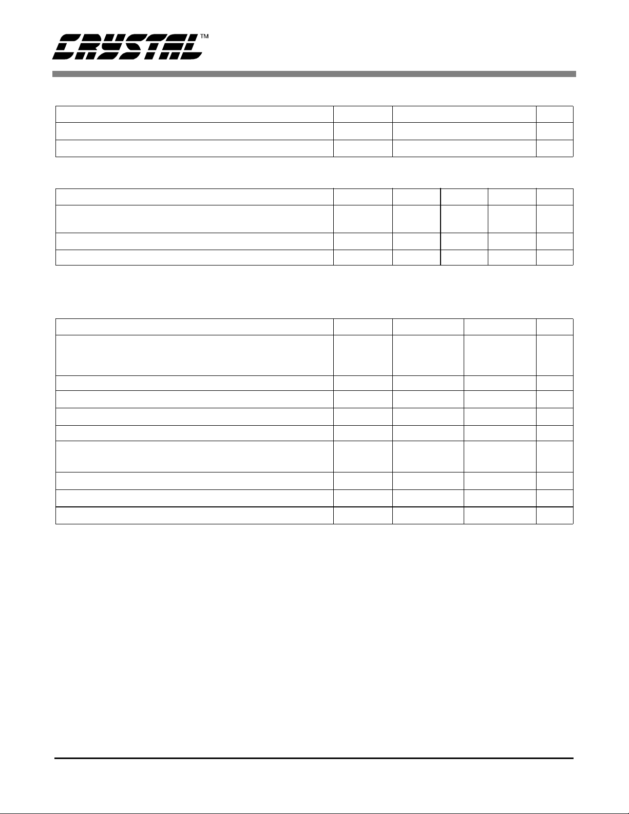
DYNAMIC CHARACTERISTICS
Parameter Symbol Ratio Unit
Modulator Sampling Frequency f
Filter Settling Time to 1/2 LSB (Full Scale S tep) t
CS5525 CS5526
s
s
XIN/2 Hz
1/f
out
s
RECOMMENDED OPERATING CONDITIONS
(AGND, DGND = 0 V; See Note 14.))
Parameter Symbol Min Typ Max Unit
DC Power Supplies Positive Digital
Positive Analog
Analog Reference Voltage (VREF+) - (VREF-) VRef
VD+
VA+
diff
2.7
4.75
5.0
5.0
5.25
5.25
1.0 2.5 3.0 V
V
V
Negative Bias Voltage NBV -1.8 -2.1 -2.5 V
Notes: 14. All voltages with respect to ground.
ABSOLUTE MAXIMUM RATINGS (AGND, DGND = 0 V; See Note 14.)
Parameter Symbol Min Max Unit
DC Power Supplies (Note 15)
Positive Digital
Positive Analog
Negative Bias Voltage Negative Potential NBV +0.3 -3.0 V
Input Current, Any Pin Except Supplies (Note 16 and 17) I
Output Current I
Power Dissipation (Note 18) PDN - 500 mW
Analog Input Voltage VREF pins
AIN Pins
Digital Input Voltage V
Ambient Operating Temperature T
Sto rage Temperature T
VD+
VA+
IN
OUT
V
INR
V
INA
IND
A
stg
-0.3
-0.3
+6.0
+6.0
V
V
-±10mA
-±25mA
-0.3
NBV - 0.3
(VA+) + 0.3
(VA+) + 0.3
V
V
-0.3 (VD+) + 0.3 V
-40 85 °C
-65 150 °C
Notes: 15. No pin should go more negative than NBV - 0.3 V.
16. Applies to all pins including continuous overvoltage conditions at the anal og input (AIN) pins.
17. Transient current of up to 100 mA will not cause SCR latch-up. Maximum input current for a power
supply pin is ±50 mA.
18. Total power dissipation, including all input currents and output currents.
WARNING: Operat ion at or beyond these limits may result in permanent damage to the device.
Normal operation is not guar anteed at these extremes.
DS202F1 5
Page 6
CS5525 CS5526
SWITCHING CHARACTERISTICS (T
Input Levels: Logic 0 = 0 V, Logic 1 = VD+; C
= 50 pF.))
L
= 25 °C; VA+ = 5 V ±5%; VD+ = 3.0 V ±10% or 5 V ± 5%;
A
Parameter Symbol Min Typ Max Unit
Master Clock Frequency (Note 19)
Internal Clock
External Clock
XIN
30
30
32.768
32.768
36
100
kHz
Master Clock Duty Cycle 40 - 60 %
Rise Times (Note 20)
Any Digital Input Except SCLK
SCLK
Any Digital Output
Fall Times (Note 20)
Any Digital Input Except SCLK
SCLK
Any Digital Output
t
t
rise
fall
-
-
-
-
-
-
50
50
-
-
-
-
1.0
100
-
1.0
100
-
µs
µs
ns
µs
µs
ns
Start-up
Oscillator Start-up Time XTAL = 32.768 kHz (Note 21) t
Power-on Reset Period t
ost
por
- 500 - ms
- 1003 - XIN
cycles
Serial Port Timing
Serial Clock Frequency SCLK 0 - 2 MHz
SCLK Falling to CS
Falling for continuous running SCLK
t
0
100 - - ns
(Note 22)
Serial Clock Pulse Width High
Pulse Width Low
t
1
t
2
250
250
-
-
-
-
ns
ns
SDI Write Timing
CS Enable to Valid Latch Clock t
Data Set-up Time pr io r to S C L K rising t
Data Hold Time After SCLK Rising t
SCLK Falling Prior to CS
Disable t
3
4
5
6
50 - - ns
50 - - ns
100 - - ns
100 - - ns
SDO Read Timi ng
CS to Data Valid t
SCLK Falling to New Data Bit t
Rising to SDO Hi-Z t
CS
7
8
9
- - 150 ns
- - 150 ns
- - 150 ns
Notes: 19. Device parameters are specified with a 32.768 kHz clock; however , clocks up to 100 kHz can be used
for increased th roughput.
20. Specified using 10% and 90% points on waveform of interest. Output loaded with 50 pF.
21. Oscillator start-up time varie s wi th cr yst al par ameter s. Thi s s pecifi cati on do es not appl y when using an
external clock source.
22. Applicable when SCLK is cont inuously running.
6 DS202F1
Page 7
CS
CS
SCLK
CS5525 CS5526
t
0
t
t
t
3
1
t
2
Continuous Running SCLK Timing (Not to Scale)
t
3
6
CS
SDO
SCLK
SCLK
t
7
MSB
MSB
MSB-1 LSBSDI
t
4
t
5
t
1
t
2
t
6
SDI Write Timing (Not to Scale)
t
9
MSB-1 LSB
t
8
t
2
t
1
SDO Read Timing (Not to Scal e)
DS202F1 7
Page 8
CS5525 CS5526
GENERAL DESCRIPTION
The CS5525 and CS55 26 ar e 16 -bit an d 20- bit pin
compatible converters which include a chopperstabilized instrumentation amplifier input, and an
on-chip programmable gain amplifier. They are
both optimized for measuring low-level unipolar or
bipolar signals in pro cess control and med ical applicatio ns .
The CS552 5/26 also include a fou rth order deltasigma modulator, a calibration microcontroller,
eight digital filters, a 4-bit analog latch, and a serial
port. The digital fil ters provide an y one of ei ght
different outpu t update rates.
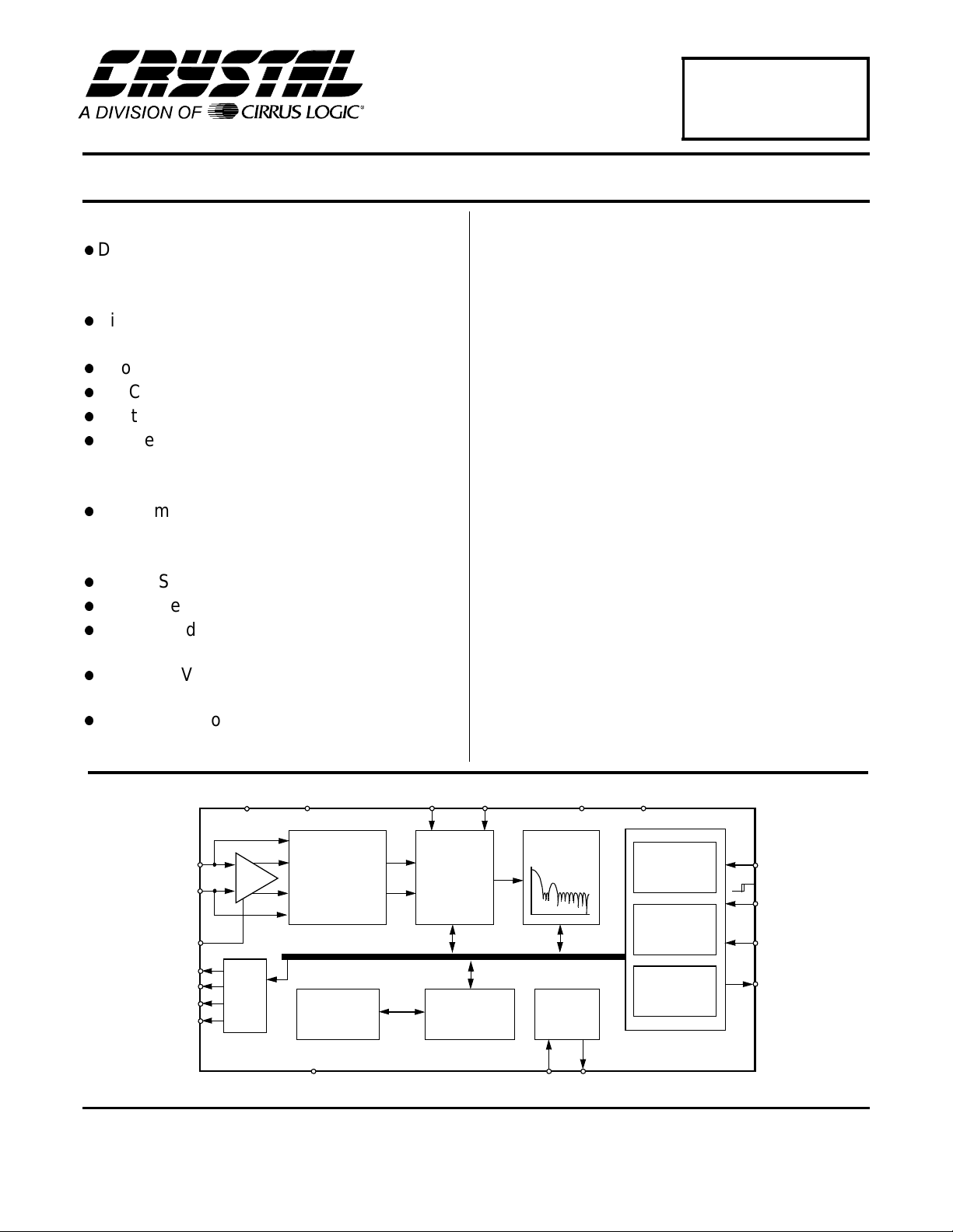
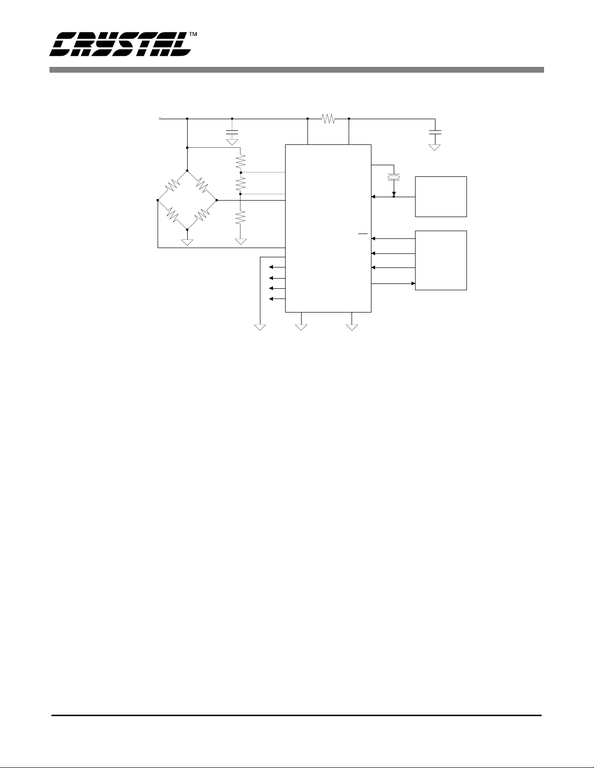
The CS5525/26 include a CPD (Charge Pump
Drive) output (shown in Figure 1). CPD provides a
negative bias voltage to the on-chip instrumentation amplifier when used with a combination of external diodes and capacitors. This enables the
CS5525/26 to me asure negative voltag es with re-
spect to ground, making the converters ideal for
thermocou p l e te mperature measurement s .
Theory of Operation
The CS5525/26 A/D converters are designed to operate from a single +5 V analog supply and provide
several different input ranges. See the Analog
Characteristics section on page 3 for details.
Figure 1 illustrates the CS5525/26 connected to
generate their o wn negative bias supply using the
on-chip CPD (Charge Pump Drive). This enables
the CS5525/ 26 to measure ground referenc ed signals with magnitudes down to NBV (Negative Bias
Voltage, approximately -2.1 V in this example).
Figure 2 illustrates a charge pump circuit when the
converters are p owered from a +3.0 V di gital sup ply. Alternative ly, the ne gative bi as supply c an be
generated from a negative supply voltage or a resistive divider as illustrated in Fig ure 3.
+5V
Analog
Supply
2.5V
Up to ± 100 mV Input
10 k
Ω
0.1 µF
Ω
10 k
Note: Cold-junction
measurement is performed
by a second A/D or via a
multiplexer.
Logic Outputs:
A0 - A3 Switch from VA+ to AGND.
0.1 µF0.1
BAV199
20
19
3
4
1
16
15
7
6
10 µF
10
Ω
213
VA+
VREF+
VREF-
AIN+
AINAGND
A3
A2
A1
A0
1N4148
+
VD+
CS5525
CS5526
CPD
8
*5MΩ
0.015 µF
1N4148
XOUT
XIN
CS
SCLK
SDI
SDO
DGNDNBV
10
32.768 ~ 100 kHz
9
18
11
17
14
125
*
Optional, see Charge
Pump Drive section.
Charg e-pump ne twork
for VD+ = 5V only and
XIN = 32.768 kHz.
Optional
Source
Serial
Interface
µ
F
Clock
Data
Figure 1. CS5525/26 Configured to use on-chip charge pump to supply NBV.
8 DS202F1
Page 9
CS5525 CS5526
F
Figure 4 illustrates the CS5525/26 connected to
measure ground referenced unipolar signals of a
positive polarity using the 1 V, 2.5 V, and 5 V input
voltage ranges on the converter. For the 25 mV, 55
mV, and 100 mV ranges the signal must have a
common mo de nea r +2.5 V (NBV = 0V).
The CS5525/26 are optimized for the measurement
of thermocouple outputs, but they are also well
suited for the measurement of ratiometric bridge
transducer outputs. Figure 5 illustrates the
CS5525/26 c onnected to measure the output of a
ratiometric differential bridge transducer while operating from a single +5 V supply .
2N5087
or similar
NBV
10µF
+
Figure 2. Charge Pump Drive Circuit for VD+ = 3 V. Figure 3. Alternate NBV Circuits.
-5V
34.8K
30.1K
2.0K
NBV
2.1K
-5V
+
10
µ
10
+5V
Analog
Supply
2.5V
0 to +5V Input
CM = 0 to VA+
0.1 µF
+
-
20
19
3
4
1
16
15
7
6
VREF+
VREF-
AIN+
AIN-
AGND
A3
A2
A1
A0
Ω
213
VA+
5
CS5525
CS5526
CPD
8
VD+
XOUT
XIN
CS
SCLK
SDI
SDO
DGNDNBV
12
10
32.768 ~ 100 kHz
9
18
11
17
14
0.1
Optional
Clock
Source
Serial
Data
Interface
Figure 4. CS5525/26 Configured for ground-referenced Unipolar Signals.
µ
F
DS202F1 9
Page 10
+5V
Analog
Supply
CS5525 CS5526
10
Ω
0.1 µF
213
CS5525
CS5526
CPD
8
VD+
XOUT
SCLK
SDO
DGNDNBV
XIN
CS
SDI
12
10
32.768 ~ 100kHz
9
18
11
17
14
VA+
20
VREF+
19
30mV
F.S.
+
3
16
15
7
6
4
1
VREFAIN+
AINAGND
A3
A2
A1
A0
5
0.1 µF
Optional
Clock
Source
Serial
Data
Interface
Figure 5. CS5525/26 Configured for Single Supply Bridge Measurement.
System Initialization
When powe r t o the CS5525/26 is ap pl ie d, they are
held in a reset cond ition until their 32 .768 kHz oscillators have started and their start-up counter-timer elapses. Due to the high Q of a 32.768 kHz
crystal, the oscillators take 400-600 ms to start. The
converter’s counter-timer counts no more than
1024 oscillator clock cycles to make sure the oscillator is fully stable. During this time-out period the
serial port logic is reset and the RV (Re set Valid)
bit in the configuration register is set. A reset can be
initiate d at an y tim e by wri ti ng a l og ic 1 t o the R S
(Reset System) bit in the configuration register.
This aut omatic all y sets th e RV bit u ntil th e RS b it
is writte n to lo gic 0, and the c on fig ura tion regi st er
is read. After a reset, the on-chip registers are initialized to the following s tates and the conv erters
are ready to perform conversion s.
Command Operation
The CS5525/26 include a microcontroller with five
registers used t o co ntr ol th e conve rter. Ea ch regi ster is 24-bits in length except the 8 -bit command
register (command, configuration, offset, gain, and
conversion data). After a system initialization or reset, the serial port is initialized to the command
mode and t he converter stays in thi s mode until a
valid 8-bit command is received (the first 8-bits
into the serial port). Table 1 lists all t h e va lid commands. Once a valid 8-bit command (a read or a
write comma nd word) is received and i nterpreted
by the comma nd register, the seria l port ent ers the
data mode. In data mode the next 24 serial clock
pulses shift data e it he r i nto or out of the se rial port
(72 serial clock pul ses a re needed if set- up re gi ster
is selected). See Table 2 for configuring the
CS5525/26.
configuration register: 000040(H)
offset register: 000000(H)
gain register: 800000(H)
10 DS202F1
Page 11
CS5525 CS5526
Reading/Writing On-Chip Registers
The CS5525/26’s offset, gain, and configuration
registers are read/writable while the conversion
data register is read only.
CC, and PS/R bi ts must be logic 0 and the CB (MSB)
bit must be a logi c 1. The r egister to be written is selected with the RSB2-RSB0 bits of the command
word. Figure 6 illustrates the serial sequence necessary to write to, or read from the serial port.
To perform a read from a specific register, the R/W
bit of the command word must be a logic 1. The SC,
CC, and PS/R
bits must be logic 0 and the CB
(MSB) bit must be a logic 1. The register to be written is selected with the RSB2-RSB0 bits of the
command word.
If the Set -up R egist ers ar e ch osen wi th t he R SB2RSB0 bits, the re gisters are re ad or written in t he
following sequ ence: Offset, Gain and Config uration. Th is is a ccomp lish ed by follow ing o ne 8-b it
command word with three 2 4-bit data words for a
total of 72 dat a bits.
To perform a writ e to a specific registe r, the R/W
bit of the command word must be a lo gic 0. The SC,
Command Register
D7(MSB)D6D5D4D3D2D1D0
CB SC CC R/W RSB2 RSB1 RSB0 PS/R
BIT NAME VALUE FUNCTION
D7 Command Bit, CB 0
D6 Single Conversion, SC 0
D5 Continuous Conversions,
CC
D4 Read/Write, R/W 0
D3-D1 Register Select Bit,
RSB2-RSB0
D0 Power Save/Run, PS/R 0
000
001
010
011
100
101
110
111
Table 1. Command Set
1
1
0
1
1
1
Null command (no operation). All command bits, including
CB must be 0.
Logic 1 for executable commands.
Single Conversion not active.
Perform a conversion.
Continuous Conversions not active.
Perform conversions continuously.
Write to selected register.
Read from selected register.
Offset Register
Gain Register
Configuration Register
Conversion Data Register (read only)
Set-up Registers (Offset, Gain, Configuration)
Reserved
Reserved
Reserved
Run
Power Save
DS202F1 11
Page 12
CS5525 CS5526
Confi
guration Register
D23(MSB) D22 D21 D20 D19 D1 8 D17 D16 D15 D14 D13 D12
A3 A2 A1 A0 NU CFS NU LPM WR2 WR1 WR0 U/B
D11 D10 D9 D8 D7 D6 D5 D4 D3 D2 D1 D0
G2 G1 G0 PD RS RV PF PSS DF CC2 CC1 CC0
BIT NAME VALUE FUNCTION
D23-D20 Latch Outputs, A3-A0 0000 R* L atch Output Pins A3-A0 mimic the D23-D20 Register bits.
D19 Not Used, NU 0 R Must always be logic 0.
D18 Chop Frequency Select,
CFS
D17 Not Used, NU 0 R Must always be logic 0.
D16 Low Power Mode, LPM 0
D15-D13 Word Rate, WR2-0
Note: For
XIN = 32.768kHz
D12 Unipolar/Bipolar, U/B 0
D11-D9 Gain Bits, G2-G0 000
D8 Pump Disable, PD 0
D7 Reset System, RS 0
D6 Reset Valid , RV 0
D5 Port Flag, PF 0
D4 Power Save Select, PSS 0
D3 Done Flag, DF 0
D2-D0 Ca libration Control Bits,
CC2-CC0
0
1
1
000
001
010
011
100
101
110
111
1
001
010
011
100
101
110/111
1
1
1R
1
1
1
000
001
010
011
100
101
110
111
R 256 Hz Amplifier chop frequency
32768 Hz Amplifier chop frequency
R Normal Mode
Reduced Power mode
R 15.0 Hz (2182 XIN cycles)
30.1 Hz (1090 XIN cycles)
60.0 Hz (546 XIN cycles)
123.2 Hz (266 XIN cycles)
168.9 Hz (194 XIN cycles)
202.3 Hz (162 XIN cycles)
3.76 Hz (8722 XIN cycles)
7.51 Hz (4362 XIN cycles)
R Bipolar Measurement mode
Unipolar Measurement mode
R 100 mV (assumes VREF = 2.5V)
55 mV
25 mV
1V
5.0 V
2.5 V
Not Used.
R Charge Pump Enabled
For PD = 1, the CPD pin goes to a Hi-Z output state.
R Normal Operation
Activate a Reset cycle. To return to Normal Operation write bit to zero.
No reset has occurred or bit has been cleared (read only).
Valid Reset has occurred. (Cleared when read.)
R Port Flag mode inactive
Port Flag mode active
R Standby Mode (Oscillator active, allows quick power-up)
Sleep Mode (Oscillator inactive)
R Done Flag bit is cleared (read only).
Calibration or Conversion cycle completed (read only).
R Normal Operation (no calibration)
Offset -- Self-Calibration
Gain -- Self-Calibration
Offset Self-Calibration followed by Gain Self-Calibration
Not used.
Offset -- System Calibration
Gain -- System Calibration
Not Used.
* R indicates the bit value after the part is reset
Table 2. Configuration Register
12 DS202F1
Page 13
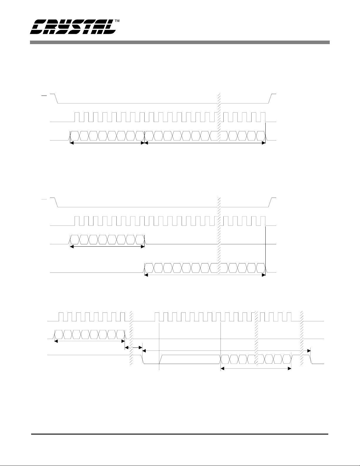
CS
SCLK
CS5525 CS5526
SDI
CS
SCLK
SDI
SDO
Command Time
8 SCLKs
Command Time
8 SCLKs
MSB
Write Cycle
MSB
Read Cycle
LSB
Data Time 24 SCLKs
(or 72 SCLKs for Set-up Registers)
LSB
Data Time 24 SCLKs
(or 72 SCLKs for Set-up Registers)
SCLK
SDI
t *
Command Time
8 SCLKs
SDO
* td = XIN/OWR clock cycles for each conversion except the
first conversion which will take XIN/OWR + 7 clock cycles
d
SDO Continuous Conversion Read (PF bit = 1)
8 SCLK s Clear SDO Flag
MSB
Data Time
24 SCLKs
XIN/OWR
Clock Cycles
LSB
Figure 6. Command and Data Word Timing.
DS202F1 13
Page 14
CS5525 CS5526
Analog Input
Figure 7 illustr ates a blo ck diagr am of t he analog input signal path inside the CS5525/26. The front end
consists of a chopper-stabilized instrumentation amplifier with 20X gain and a programmable gain section. The instrumentation amplifie r is powered from
VA+ and from the NBV (Negative Bias Volt age) pin
allowing the CS5525/26 to be operated in either of
two analog input configurations. The NBV pin can
be biased to a negative voltage between -1.8 V and
-2.5 V, or tied to AGND. The choice of the operating
mode for the NBV voltage depends upon the input
signal and its common mode voltage.
For the 25 mV, 55 mV, and 100 mV input ranges, the
input signals to AIN+ and AIN- are amplified by the
20X instrumentation amplifier. For ground referenced signals with magnitudes less then 100 mV, the
NBV pin should be biased with -1.8 V to -2.5 V. If
NBV is tied between -1. 8 V and -2.5 V, the (Com mon Mode + Signal) input on AIN+ and AIN- must
stay between -0.150 V and 0.950 V to ensure proper operation. Alternatively, NBV can be tied to
AGND where the input (Common Mode + Signal)
on AIN+ and AIN- must stay b etween 1.85 V and
2.65 V to ensure tha t the ampl ifier ope rates prop erly.
For the 1 V, 2.5 V, and 5 V input ranges, the instrumentation amplifi er is bypassed and the input signals are directly connected to the Programmable
Gain block. With NBV tied between -1.8 V and
-2.5 V, the (Common Mode + Signal) input on
AIN+ and AIN- must stay between NBV and VA+.
Alternatively, NBV can be tied to AGND where
the input (Com mon Mode + Sig nal) on AIN+ and
AIN- pins can span the entire range between
AGND and VA+.
The CS5525/26 can accommodate full scale ranges
other than 25 mV, 55 mV, 100 mV, 1 V, 2.5 V and
5 V by performin g a syste m calibr ation wi thin the
limits specified. See the Calibration section fo r
more details. Another way to change the full scale
range is to increase or to decrease the voltage reference to ot her than 2.5 V. Se e the Vo ltage Refer-
ence sectio n for more detail s.
Three factor s set the op erating limits for t he input
span. They include: instrumentation amplifier satu-
ration, modulator 1’s density, and a lower reference
voltage. When the 25 mV, 55 mV or 100 mV range
is selected, the input signal (including the common
mode voltage and the amplifier offset voltage)
must not caus e the 20 X amp lifier to saturat e in ei ther its inp ut s tag e o r outpu t s tage . To pre vent sat uration the absolute voltages on AIN+ and AINmust stay within the limits specified (refer to the
‘Analog Input’ table on pag e 3). Addit ional ly, t he
differential output voltage of the amplifier must not
exceed 2.8 V. The equation
ABS(VIN + VOS) x 20 = 2.8 V
defines the diffe rential output li mit, where
VIN = (AIN+) - (AIN-)
is the differentia l input volt age and VOS is the absolute maximum offset voltage for the instrumentation amplifier (VOS will not exceed 40 mV). If the
VREF+
AIN+
AIN-
NBV
14 DS202F1
X20
Figure 7. Block Diagram of Analog Signal Path
Programmable
Gain
Differential 4th
order delta-
sigma modulator
VREF-
Digital Filter
Page 15
CS5525 CS5526
F
Input Range
± 25 mV
± 55 mV
± 100 mV
± 1.0 V - 2.5V 2.5 ± 1.0 V ± 1.5 V
± 2.5 V - 2.5V 1.0 ± 2.5 V ± 5.0 V
± 5.0 V - 2.5V 0.5 ± 5.0 V 0V, VA+
Note: 1. The converter ’s actual input range, the delta-sigma’s nominal full scale input, and the delta-sigma’s
(1)
maximum full scale input all scale directly with the value of the voltage reference. The values in the
table assume a 2.5 V VREF voltage.
Table 3. Relationship between Full Scale Input, Gain Factors, and Internal Analog Signal Limitations
differential output voltage from the amplifier exceeds 2.8 V, the amplifier may saturate, which will
cause a measure ment error.
The input voltage into the modulator must not
cause the mo dulat or to exce ed a lo w of 20 perce nt
or a high of 80 percent 1’s density. The nominal full
scale input span of the modu lator (from 3 0 pe rcent
Max. Differential Output
20X Amplifier
(2)
2.8 V
(2)
2.8 V
(2)
2.8 V
VREF Gain Factor
2.5V 5 ± 0.5 V ± 0.75 V
2.5V 2.272727... ± 1.1 V ± 1.65 V
2.5V 1.25 ± 2.0 V ±3.0 V
Note: Residual nois e appear s in the conve rter’ s base band f or
output wor d rat es gr eater t han 60 Hz if CFS is logic 0. By s etting CFS to logic 1, the amplifier’s chop frequency chops at
32768 Hz eliminating the residual noise, but increasing the
current.
For physical inp ut capac itance see ‘Input Capac itance’ specification under ‘Analog Characteristics’ on page 3.
Note that C=48 pF is for i nput curr ent modeli ng only.
25mV, 55mV, and 100mV Ranges
∆-Σ Nominal
Differential Input
(1)
(1)
∆-Σ
Max. Input
to 70 percent 1’s density) is determined by the
VREF voltage divi de d by the Gain Factor. See Ta ble 3 to determine if the CS5525/26 are being used
properly. For example, in the 55 mV rang e to determine the nominal input voltage to the modulator,
divide VREF (2.5 V) by the Gain Factor (2.2727).
When a sma ller voltage referen ce is used, the re -
AIN
V ≤ 25mV
os
i = fV C
osn
CFS = 0 , f = 256 Hz
CFS = 1 , f = 32.768 kHz
C = 48p
sulting code widths are smaller causing the converter output codes to exhibit more changing codes
for a fixed amount of noi se. T able 3 i s based u pon
a VREF = 2.5 V. For other values of VREF, the values in Table 3 must be scale d a cc ordingly.
Figure’s 8 and 9 il lustrate the inp ut m odels f or t he
AIN and VREF pins. The dynamic input current for
each of the pins can be determined from the models
shown and is dependent upon the setting of the CFS
(Chop Frequency Select) bit. The effective input
AIN+
Figure 8. Input models for AIN+ and AIN- pins
1V, 2.5 V, and 5V Ranges
AIN-
i = [(V ) - (V )] fC
n
AIN+ AIN-
f = 32. 7 68 kH z
VREF+
VREF-
C = 32pF
C = 16pF
impedance for the AIN+ and AIN- pins remains
i = [(VREF+) - (VREF-)] fC
constant for the three low level measurement ranges (25 mV, 55 mV, and 100 mV). The input current
Figure 9. Input model for VREF+ and VREF- pins.
n
f = 32.768 kHz
is lowest w it h the CF S bit cleared to logic 0.
DS202F1 15
Page 16

CS5525 CS5526
Charge Pump Drive
The CPD (Charge Pump Drive) pin of the converters can be used with ext ernal component s (shown
in Figure 1) to develop an appropriate negative bias
voltage for the NBV pin. When CPD is used to generate the N BV, the NBV vol tage is regul ated with
an internal regulator loop referenced to VA+.
Therefore, any change on VA + re s u lt s in a propor-
tional change on NBV. With VA+ = 5 V, NBV’s
regulation is set proportional to VA+ at approximately -2.1 V.
Figure 3 illustrates a means of supplying NBV voltage from a -5 V supply. For groun d based signals
with the instru mentation amplifie r engaged (w hen
in the 25mV, 55mV, or 100mV ranges), the voltage
on the NBV pin should at no t ime be l ess negati ve
than -1.8 V or m ore negati ve than - 2.5 V. To prevent excessive vol tage stress to the chip the NBV
voltage should not be more nega ti ve tha n -3. 0 V.
The components in Figure 1 are the preferred components for the CPD filter. H owever, smalle r capacitors ca n be used w ith accept able resul ts. The
µF ensures very low r ipple on NBV. Int rinsic
10
safety require ment s prohi bit th e u se o f ele ctrolyt ic
capacitors. In this case, two 0.47
itors in paralle l ca n be used.
The CPD pi n itself is a tri-s tate output and enters
tri-state whenever the converters are placed into the
Sleep Mode, Standby Mode, or when the charge
pump is disabled (when the Pump Disa ble bit, bit
D8 in the configuration register, is set). Once in tristate, the digital current can increase if this CPD
output floats near 1/2 digital supply. T o ensure the
CPD pin stays near ground and to minimize the
digital cur rent, a dd a 5MΩ re sistor be tween it and
DGND (see Figure 1). If the resistor is left out, the
digital supply current may increase from 2 µA to 10
µA.
µF ceramic capac-
Voltage Reference
The CS5525/ 26 are speci fied for ope ration wit h a
2.5 V reference voltage between the VREF+ and
VREF- pins of the devices. For a single-ended reference volta ge, such as t he LT1019-2 .5, the refer ence’s output is connected to the VREF+ pin of the
CS5525/26. The ground referenc e for the LT1019-
2.5 is connec te d to the VREF- pin.
The differential voltage between the VREF+ and
VREF- can be any vo lt age from 1.0 V up to 3.0 V,
however, the VRE F- pin can not go belo w analog
ground.
Calibration
The CS5525/26 offer five different calibration
functions including self calibration and system calibration. How ever, after the CS 5525/26 are reset,
they can perform measurements without being calibrated. In this case, th e convert ers will uti lize the
initialize d values of the on-chip regi sters (Gain =
1.0, Offset = 0.0) to ca lcula te out put wor ds for the
±
100 mV ra nge. Any in itial offset and g ain errors
in the internal circuitry of the chips will remain.
The gain and offset registers, which are used for
both self and system calibration, are used to set the
zero and full-scale points of the converter’s transfer
-24
-23
). The
i–
2
i
pro-
function. One LSB in the offset register is 2
portion of the input span (bipolar span is 2 times the
unipolar span). Th e MSB in the offset reg ister determines i f the offset to be trimmed is p ositive or
negative (0 positive, 1 negative). The converters
can typically trim ±50 percent of the input span.
The gain register spans from 0 to (2 - 2
decimal equ iva lent meaning of the gain regi ste r is
N
Db020b121–b222–…bN2
==
++++ b
N–
∑
i0=
where the binary numbers have a value of either
zero or one (b
4 for details.
Table
corresponds to the MSB ). Refer to
0
16 DS202F1
Page 17

CS5525 CS5526
Offset Register
MSB LSB
-2
-3
-4
-5
Register
Reset (R) 0 00000 0 0 0 0 0 0
Sign
2
2
2
2
-6
2
-19
2
-20
2
-21
2
-22
2
-23
2
≈
-24
2
One LSB represents 2
-24
proportion of the input span (b ipolar span is 2 times unipolar span)
Offset and data word bits align by MSB (bit MSB-4 of offset register changes bit MSB-4 of data)
Gain Register
MSB LSB
0
-1
-2
-3
-4
Register
Reset (R) 1 00000 0 0 0 0 0 0
The gain register span is from 0 to (2-2
2
2
2
2
2
-23
). After Reset the MSB = 1, all other bits are 0.
-5
2
Table 3.
Table 4. Offset and Gain Registers
The offset and gain cal ibration steps each take one
conversion cycle to complete. At the end of the calibration step, the calibration control bits will be set
back to logic 0, and the DF (D one Flag) bit w il l be
set to a logic 1. For the combination self-calibration (CC2-CC0= 011; offset followed by gain), the
calibration will take two conversion cycles to complete and wil l set the DF bi t after t he gain c alibra tion is comple ted. The DF bit will be cl eared any
time the d ata register , the offset r egister, the gain
register, or the set up register is rea d. Reading the
configuration register alone will not clear the DF
bit.
-18
2
-19
2
-20
2
-21
2
-22
2
≈
of the modulat or are connected together and then
routed to the VREF - pin as shown i n Figure 11.
For self-calibrat ion of gain, the differentia l inputs
of the modulator are connected to VREF+ and
S1
OPEN
AIN+
AIN-
S2
CLOSED
+
X20
-
-23
2
+
-
Self Calibration
Figure 10. Self Calibration of Offset (Low Ranges).
The CS5525/ 26 offer b oth sel f o ffset a nd sel f gain
calibrations. For the self-calibration of offset in the
25 m V, 55 m V, and 100 mv ranges, the conv erter
internally ties the inputs of the instrumentation amplifier toge the r and rou tes them to the AIN- pi n as
shown in Figure 10. For pro per self-ca libration o f
offset to occur in the 25 mV , 55 mV, and 100 mV
AIN+
AIN-
VREF-
+
X20
-
ranges, the AIN- pin must be at the proper common-mode-vol tage (i.e . AIN- = 0V, NBV must be
between -1.8 V to -2.5 V). For self- calibration of
offset in the 1.0 V, 2.5 V, and 5 V ranges, the inputs
DS202F1 17
Figure 11. Self Calibration of Offset (High Ranges).
S1
OPEN
S2
OPEN
S4
CLOSED
+
S3
CLOSED
-
Page 18

Reference
+
-
AIN+
AIN-
VREF+
VREF-
CS5525 CS5526
OPEN
+
X20
OPEN
CLOSED
CLOSED
+
-
External
Connections
+
0V
-
+
CM
-
AIN+
AIN-
+
X20
-
+
-
Figure 12. Self Calibration of Gain (All Ranges).
VREF- as shown in Figure 12. For any input range
other than the 2.5 V range, the modulator gain error
can not be completely calibrated out. This is due to
the lack of an accurate full scale voltage internal to
the chips . T he 2.5 V range is an exceptio n be cause
the external reference voltage is 2.5 V nominal and
is used a s the full s cale volta ge. In additi on, w hen
self-calibrat io n of gain is pe rfor med in the 25 mV,
55 mV, and 100 mV input ranges, the instrumenta-
tion amplifier’s gain is not calibrated. These two
factors can leave the converters with a gain error of
up to ±20% after self-calibration of gain. Therefore, a system ga in i s required to get better ac curacy, except for the 2.5 V range .
System Calibration
For the system calibration functions, the user must
supply the converters calibration signals which represent ground and full sc al e. When a system offset
calibration is performed , a ground ref ere nce signal
must be applied to the converter. See Figures 13
and 14. As shown in Figures 15 and 16, the user
must input a signal representing the positive full
scale point to perform a system gain calibration. In
either ca se, the cali bration signal s must be w ithin
the specified calibration limits for each specific
calibration step (refer to the System Calibration
Specifications).
Figure 13. System Calibration of Offset (Low Ranges).
External
Connections
0V
CM
AIN+
+
-
AIN-
+
-
+
X20
-
+
-
Figure 14. System Calibration of Offset (High Ranges).
External
Connections
+
X20
-
Full Scale
CM
AIN+
+
-
AIN-
+
-
Figure 15. System Calibration of Gain (Low Ranges)
External
Connections
+
X20
-
Full Scale
CM
AIN+
+
-
AIN-
+
-
+
-
+
-
Figure 16. System Calibration of Gain (High Ranges).
18 DS202F1
Page 19

CS5525 CS5526
Assuming a system can provide two known voltages, equation s can allow the us er to m anual ly co m-
pute the calib ration reg ister’s val ues based on two
uncalibrate d c onversions. The offset and g ai n calibration registers are used to adjust a typical conversion as follows:
23
Rc = (Ru + Co>>4) * Cg / 2
.
Calibration can be performed using the follow ing
equations:
Co = (Rc0/G - Ru0) << 4
23
Cg = 2
* G
where G = (Rc1 - Rc0)/(Ru 1-Ru0).
Note: Uncalibr ated conv ersions imply t hat the gain and offset
registers are at default {gain register = 0x800000 (Hex) and
offset register = 0x000000 (Hex)}.
The variables are defined below.
V0 = First calibration voltage
V1 = Second calibration voltage (greater than V0)
Ru = Result of any uncalibrated conversion
Ru0 = Result of uncalibrated conversion V0
(20-bit integer or 2’s complement)
Ru1 = Result of uncalibrated conversion of V1
(20-bit integer or 2’s complement)
Rc = Result of any conversion
Rc0 = Desired calibration result of converting V0
(20-bit integer or 2’s complement)
Rc1 = Desired calibration result of converting V1
(20-bit integer or 2’s complement)
Co = Offset calibration register value (24-bit 2’s
complement)
Cg = Gain calibration register value
(24-bit integer)
>> = The shift right operator (e.g. x >>2 is x shift-
ed right 2 bits)
<< = The shift left operator (e.g. x<<2 is x
shifted left 2 bit s)
Note: The shift operators are used here to align the decimal
points of words of various lengths. Data to the right of the
decimal point may be used in the c al cul at ion s s hown. For the
CS5525 all conversion results (Ru, Rc...) are 16 bits instead
of 20 bits. To get the equations to work correctly pad the 16
bit results with four zeros (on the right).
Calibration Tips
Calibration step s are perfo rm ed at th e ou tput word
rate selected by the WR2-WR0 bits of the configuration register. Since higher word rates result in
conversion words with more peak-to-peak noise,
calibration should be performed at lower output
word rates. Also, to minimize digital noise near
the devices, the user should wait fo r each calibration step to be completed before reading or writing
to the serial port.
For maximum accuracy, calibrations should be performed for offset and gain for each gain setting (selected by changing the G2-G0 bits of the
configuration register). And if factory calibration is
performed using the system calibration capabilities
of the CS5525/26 , the offset and ga in register contents can be read by the system microcontroller and
recorded in EEPROM. These same calibration
words can then be uploaded into the offset and gain
registers of the conv erters when power is first ap plied to the system, or when the gain range is
changed.
Two final tips include two ways to determine when
calibration is com plete : 1) wait for SDO to fal l. It
falls to logic 0 if the PF (Port Flag) bit of the configuration register is set to logic 1; or 2) poll the DF
(Done Flag) bit in t he configuration register which
is set at completion of calibration. Whichever
method is u sed, the ca libration c ontrol bits (C C2CC0) will return to logic 0 upon completion of any
calibration.
Limitations in Calibration Range
System ca libration can be limited by sig nal headroom in the analog signal path inside the chip as
discussed under the Analog Input section of this
data sheet . System cal ibration can al so be limited
by the intrinsic ga in errors of the instrumentat ion
amplifier a nd the mo dulator. Fo r gain ca libratio ns
DS202F1 19
Page 20

CS5525 CS5526
the input signal can be reduced to the point in
which the gain register reac hes its upper limi t of 2.0
(decimal) [FFFFFF Hex] (this is most likely to occur with an input signal approximately 1/2 the
nominal rang e). Alte rna tive ly, the in put sig nal c an
be increased to a point in which the modulator
reaches its one’s density upper limit of 80% (this is
most likely to occur with an in put signal approxi mately 1.5 times the no minal ra ng e). Also, for full
scale inputs larger than the nominal full scale value
of the range selected, there is some voltage at
which the various internal circuits may saturate due
to limited amplifier headroom (this is most likely to
occur on the 100 mV range setting when NBV = -
1.8 V).
Analog Output Latch Pins
The A3-A0 pin s of the conve rters m imic th e D23D20 bits of the configu ration register. A3-A0 can
be used to control multiplexers and other logic
functions outside the converter. The outputs can
sink or source at least 1 mA, but it is recommended
to limit drive currents to less than 20µA to redu ce
self-heat ing of the chip. Thes e outputs are power ed
from VA+, hence, their output voltage for a logic 1
will be limi t ed to the VA+ vo ltage.
Serial Port Interface
The CS5525/26 serial interface consist of four pins,
SCLK, SDO, SDI, and CS
held low (logic 0) before SCLK tra nsitions c an be
recognized by the port logic. The SDO output will
be held at high impedance any time CS
If the CS
three wire interface.
The SCLK inpu t is desi gned wi th a Sc hm itt- tri gger
input to al lo w an opto is olat or w ith s low er ri se and
fall times to directl y drive the pin.
The SDO output is c apable of si nking or sourc ing
up to 5 mA to directl y drive a n optois olator LE D.
SDO will have less than a 400 mV loss in t he drive
voltage when sink ing or sourcing 5 mA.
pin is tied low, th e por t can func tion as a
. The CS pin must be
is a logic 1.
Serial Port Initialization
The serial port is initialized to the command mode
whenever a powe r-on reset is performed inside the
converter, whe n the port initia lization sequenc e is
completed, or whenever a command byte, data
word sequence is completed. The port initialization
sequence in volves clocking 15 (or m ore) bytes of
all 1's, f ollowed by one byte w i th the foll ow ing bit
contents (11111110). This sequence places the
chips in the command m ode where it w aits for a
valid command.
Performing Conversions (With PF bit = 0)
Setting the SC (Single Conversion) bit of the command word to a logic 1 with the CB bit = 1, all other
command bits = 0, the CS5525/CS5526 will perform one conversion. At the completion of the conversion the DF (Done Flag) bit of the configuration
register wi ll be set t o a logi c 1. The us er can re ad
the configuration register to determine if the DF bit
is set. If DF has been set, a command can be issued
to read the conversion data register to obtain the
conversion data word. Th e DF bit of the c onfiguration regist er will be cleare d to logic 0 when the
data register, the gain register, the offset register, or
the set-up registers are read. Reading only the configuration regi ster will not cle ar th e DF fl ag bi t.
If an SC command is issued to the converters while
they are performing a conversion, the filter will restart a co nvol ution cycle t o perform a ne w conversion.
Performing Conversions (With PF bit = 1)
Setting the PF bit of th e c onfigu rati on regi ste r to a
logic 1 enables the SDO output pin to behave as a
flag signal whenever conversions are completed.
This eliminates the need for the user to read the DF
flag bit of the configuration register to determine if
the conversion data word is available.
If the SC (Single Conversion) com mand is issued
(SC = 1, CB= 1, all othe r command bits = 0) the
SDO pin will go low at the completion of a conver-
20 DS202F1
Page 21

CS5525 CS5526
sion. The user would then issue 8 SCLKs (with
SDI = logic 0) to clear the SDO flag. Upon the falling edge of the 8th SCLK, the SDO pin will present
the first bit (MSB) of the conversion word. 24
SCLKs (high, then low) are required to read the
conversion word from the port. Th e user must not
give an explicit command to read the conversion
data regist er wh en t he P F bit is set to logic 1. Th e
data conversion word must be read before a new
command can be entered (if the SC command is
used with PF = 1).
If the CC (Continuous Conversion) command is issued (CC = 1, CB =1 , all o the r com man d bit s = 0 )
the SDO pin will go low at the completion of a conversion. The user would then issu e 8 SCLKs (with
SDI = logic 0) to clear the SDO flag. Upon the falling edge of the 8th SCLK, the SDO pin will present
the first bit (MSB) of the conversion word. 24
SCLKs (high, then low) are required to read the
conversion word from the port . The user must not
give an explicit command to read the conversion
data regist er when the PF bit is set to lo gic 1. Whe n
operating in the continuous conversion mode , the
user need not read every conversion. If the user
does nothing after SDO falls, SDO will rise one
XIN clock cycle before the next conversion word is
availabl e and then fall again to sign al that a nother
conversion word is availabl e. If the us er begins to
clear the SDO flag and read the conversion data,
this actio n must be finishe d before the con version
cycle which is occurring in the background is complete if the user wants to be able to read the new
conversion da ta.
To exit the con ti nuous conversion m ode, issue any
valid command to the SDI input when the SDO flag
falls. If a C C command is is sued to the conv erter
while it is pe rforming a conversion, th e filter will
restart a convo lution cycle to perfor m a new conversion.
Output Word Rate Selection
The WR2-WR0 bits of the configuration register
set the output conversion word ra te of the co nverters as shown in Table 2. The word rates indicated
in the table a ssume a mas ter clock of 3 2.768 kHz.
Upon reset the converters are set to operate with an
output word rate of 15.0 Hz.
Clock Generator
The CS5525/26 include a gate which can be connected with an external cry stal to p rovide th e master
clock for the chips. They ar e designed to o perate us-
ing a low-cost 32.768 kHz “tuning fork” type crystal. One lead of the crystal should be connected to
XIN and the other to XOUT. Lead lengths should be
minimized to reduce stray capa citance.
The converters will operate with an external
(CMOS compa tible) clock with f requencies up to
three times the typi cal crysta l frequenc y of 32.768
kHz. Figure 17 details the converter’s performance
at increased clock rates.
Figure 17. High Speed Clock Performance
The 32.768 kHz crystal is normally specified as a
time-keeping crystal with tight specifications for
both initial fr eque ncy and for drif t over temperatu re.
To maintain excellent frequency stability, these
crystals are specified only over limited operating
temperature ranges (i.e. -10 °C to +60 °C). However,
applications with the CS55 25/26 don’t generally require such tight tolerances. When 32.768 kHz surface mount crystals are used, it is recommended that
protection components, an external resistor and capacitor as shown in Figure 18, be used.
DS202F1 21
Page 22

CS5525 CS5526
VA+ VD+
XOUT
CS5525
CS5526
Figure 18. Surface Mount Crystal Connection Diagram
500 k
XIN
Ω
20 pF
32.768 kHz
Digital Filter
The CS5525/26 have eight different linear phase
digital filters which set the output word rates
(OWRs) a s stated in Table 2. Th ese rates assume
that XIN is 32.768 kHz. Each of the filters has a
magnitude response similar to that shown in Figure
19. The filters are optimized to settle to full accuracy every conversion and yield better than 80 dB rejection for both 50 and 60 Hz with output word
rates at or below 15.0 Hz.
The convert er’s digital fi lters scale wit h XIN. For
example with an output word rate of 15 Hz, the filter’s corner fre quenc y is typi call y 1 2.7 Hz . If XI N
is increased to 64 .536 kHz the O WR doubles and
the filter’s corner fre quency moves to 25 .4 Hz.
Output Coding
The CS5525/26 out put data in binary fo rm at when
operating in unipolar mode and in two's complement when operating in bipolar m ode.
The output conversion word is 24 bits, or three
bytes long, as shown in Table 5. The MSB is output
Figure 19. Filter Response
(Norma lized to Output W ord Rate = 1)
first followed by the rest of the data bits in descending order. For the CS5525 the last byte is composed
of bits D7-D4, which are al ways logic 1; D3-D2,
which are always logic 0; and bits D1-D0 which are
the two fla g bits. For the CS552 6 the last byt e includes data bits D7-D4, D3-D2 wh ich are alwa ys
logic 0 and the two flag bits.
The OF (Overra nge Flag) bit is set to a logic 1 any
time the input signal is: 1) more positive than positive full scale, 2) more negative than zero (unipolar
mode), 3) more negative than negative full scale
(bipolar mode). It is cl eared back to logic 0 when ever a conversion word occurs which is not overranged.
The OD (Oscillation Detect) bit is set to a logic 1 any
time that an oscillatory condition is detected in the
modulator. This does not occur under normal operating conditions, but may occur whenever the input
Output Conversion Data CS5525 (16 bits + flags)
D23 D22 D21 D20 D19 D18 D17 D16 D15 D14 D13 D12 D11 D10 D9 D8 D7 D6 D5 D4 D3 D2 D1 D0
MSB1413121110987654321LSB111100ODOF
Output Conversion Data CS5526 (20 bits + flags)
D23 D22 D21 D20 D19 D18 D17 D16 D15 D14 D13 D12 D11 D10 D9 D8 D7 D6 D5 D4 D3 D2 D1 D0
MSB181716151413121110987654321LSB00ODOF
Table 5. Data Conversion Word
22 DS202F1
Page 23

CS5525 CS5526
CS5525 16-Bit Output Coding CS5526 20-Bit Output Coding
Unipolar Input
Voltage
>(VFS-1.5 LSB) FFFF >(VFS-1.5 LSB) 7FFF >(VFS-1.5 LSB) FFFFF >(VFS-1.5 LSB) 7FFFF
VFS-1.5 LSB
VFS/2-0.5 LSB
+0.5 LSB
<(+0.5 LSB) 0000 <(-VFS+0.5 LSB) 8000 <(+0.5 LSB) 00000 <(-VFS+0.5 LSB) 80000
Note: VFS in the table equals the voltage bet ween ground and full scale for any of the unipolar gain ranges, or the
voltage between ±full scale for any of the bipolar gain ranges. See text about error flags under overrange
conditions.
to the converters is extremely overr anged. If the OD
bit is set, the conversion data bits can b e completely
erroneous. The OD flag bi t will be cleared t o logic 0
when the modulator becomes stable. Table 6 illus trates the output coding for t h e CS 5525/26.
Offset
Binary
FFFF
-----
FFFE
8000
-----
7FFF
0001
-----
0000
Bipolar Input
Voltage
VFS-1.5 LSB
-0.5 LSB
-VFS+0.5 LSB
Two’s
Complement
7FFF
-----
7FFE
0000
-----
FFFF
8001
-----
8000
Table 6. 5525/26 Output Coding
Unipolar Input
Voltage
VFS-1.5 LSB
VFS/2-0.5 LSB
+0.5 LSB
command wor d a re se t to lo gic 1. T he p ar ticu la r
power save mode ente red depends on state of bit
D4 (the Power Save Select bit) in the configuration
register. If D4 is logic 0, t he converte rs enters the
standby mode re ducing the p ower consumpt ion to
Offset
Binary
FFFFF
-----
FFFFE
80000
-----
7FFFF
00001
-----
00000
Bipolar Input
Voltage
VFS-1.5 LSB
-0.5 LSB
-VFS+0.5 LSB
Two’s
Complement
7FFFF
-----
7FFFE
00000
-----
FFFFF
80001
-----
80000
1.2mW. The standby mode leaves the oscillator
Power Consumption
The CS5525/26 accommodate four power consumption modes: normal, low po wer, standby, and
sleep. The no rmal mode, the defau lt mode, is entered after a power-on-reset and typically consumes 7.5 mW. The low power mode is an alter nate
mode that reduces the consumed power to 4 mW. It
is entered by se tting b it D16 (the low po wer mode
bit) in the co nfiguration register to l ogic 1. Since
the converter’s noise performance improves with
and the on-chip bias generator running. This allows
the converters to quickly return to the normal or
low power m od e once th e PS /R
bit is set back to a
logic 1. If D4 in the confi guration register and CB
and PS/R
in the com mand word are set to logic 1,
the sleep mode is entered reducing the consumed
power to less than 500 µW. Since the sleep mode
disables the oscillat or, approximatel y a 500ms oscillator sta rt-up del ay peri od is requ ired b efore re turning to the normal or low power mode.
increased power consumption, slightly degraded
noise or lineari ty performa nce should be expected
in the low power mode. The final two modes are referred to as the power save modes. They power
down most of the analog portion of the chips and
stop filter convolutions. The power save modes are
entered whenever the PS/R
bit and the CB bit of the
PCB Layout
The CS5525/ 26 should be pl aced entirel y over an
analog ground plane with both the AGND and
DGND pins of the device connected to the analog
plane. Place th e analog-d igit al plane split immedi ately adjacent to the digital portion of the chi p .
DS202F1 23
Page 24

PIN DESCRIPTIONS
CS5525 CS5526
ANALOG GROUND AGND VREF+ VOLTAGE REFERENCE INPUT
POSITIVE ANALOG POWER VA+ VREF- VOLTAGE REFERENCE INPUT
DIFFERENTIAL ANALOG INPUT AIN+ CS
DIFFERENTIAL ANALOG INPUT AIN- SDI SERIAL DATA INPUT
NEGATIVE BIAS VOLTAGE NBV A3 LOGIC OUTPUT
LOGIC OUTPUT A0 A2 LOGIC OUTPUT
LOGIC OUTPUT A1 SDO SERIAL DATA OUTPUT
CHARGE PUMP DRIVE CPD VD+ POSITIVE DIGITAL POWER
CRYSTAL IN XIN DGND DIGITAL GROUND
CRYSTAL OUT XOUT SCLK SERIAL CLOCK INPUT
1
2
3
4
5
6
7
8
9
10 11
20
19
18
17
16
15
14
13
12
CHIP SELECT
Clock Generator
XIN; XOUT - Crystal In; Crystal Out, Pins 9, 10.
A gate inside the chip is conn ected to these pins a nd can be used with a crystal to provi de the
master clock for the device. Alternatively, an external (CMOS compatible) clock can be
supplied into t he XIN pin to pro vide the m aster clock for the device .
Control Pins and Serial Data I/O
CS - Chip Select, Pin 18.
When active low, the port will recognize SCLK. When high the SDO pin will output a high
impedance s tate. C S
should be changed wh en SCLK = 0 .
SDI - Serial Data Input, Pin 17.
SDI is the input pi n of the seria l input port . Data will be input at a rat e determine d by SCLK.
SDO - Serial Data Ou tput, Pin 14.
SDO is the serial data output. It will output a high impedance state if CS
SCLK - Serial Clock Input, Pin 11.
A clock signal on this pin determines the input/output rate of the data for the SDI/SDO pins
respective ly. Th is input is a Schmitt trig ger to allow for slow rise time signals. Th e SCLK pin
will recogniz e clocks onl y when CS
is low.
A0, A1, A2, A3 - Logic Outputs, Pin 6, 7, 15, 16.
The logic states of A0-A3 mimic the states of the D20-D23 bits of the configuration register.
Logic Output 0 = AGND, and Logic Output 1 = VA+.
= 1.
24 DS202F1
Page 25

Measurement and Reference Inputs
AIN+, AIN- - Differential Analog Input, Pins 3, 4.
Differential input pins into the device.
VREF+, VREF- - Vo ltage Reference Input, Pins 20, 19.
Fully differential i nputs which e stablish the voltage re ference for the on-chip mod ulator.
NBV - Negative Bia s Voltage, Pin 5.
Input pin to supply the negative supply voltage for the 20X gain instrumentation amplifier.
May be tied to AGND if AIN+ and AIN- inputs are centered around +2.5 V; or it may be tied
to a negati ve supply voltag e (-2.1 V typical ) to allow the am plifier to handle low level signal s
more negative t han ground.
CPD - Charge Pump Drive, Pin 8.
Square wave outp ut used to provide ene rgy for the charge pum p.
Power Supply Connections
CS5525 CS5526
VA+ - Positive Anal og Power, Pin 2.
Positive analog supply voltage. Nominally +5 V.
VD+ - Positive Digital Power, Pin 13.
Positive digital supp ly voltage . Nominally +3. 0 V or +5 V.
AGND - Analog Ground, Pin 1.
Analog Ground.
DGND - Digital Ground, Pin 12.
Digital Ground.
DS202F1 25
Page 26

SPECIFICATION DEFINITIONS
Linearity Error
The deviation of a code from a straight line which connects the two endpoints of the A/D
Converter transfer function. One endpoint is located 1/2 LSB below the first code transition
and the other endpoint is located 1/2 LSB beyond the code transition to all ones. Units in
percent of full -scale.
Differential Nonline arity
The deviati on of a code’s wi dth from the ideal width. Units in LSBs.
Full Scale Error
The deviation of the last code transition from the ideal [{(VREF+) - (VREF-)} - 3/2 LSB].
Units are in LSBs.
Unipolar Offset
The deviation of the first code transition from the ideal (1/2 LSB above the voltage on the
AIN- pin.). When in un ipolar mode (U/B
CS5525 CS5526
bit = 1). Units are in LSBs.
Bipolar Offset
The deviation of the mid-scale tra nsition (111...111 to 000...000) from th e ideal (1/2 LSB belo w
the voltag e on the A IN- pin). When in bi polar mo de (U/B
ORDERING GUIDE
Model Number Linearity Error (Max) Temperature Range Package
CS5525-AP ±0.003% -40°C to +85°C 20-pin 0.3" Plastic DIP
CS5525-AS ±0.003% -40°C to +85°C 20-pin 0.2" Plastic SSOP
CS5526-BP ±0.0015% -40°C to +85°C 20-pin 0.3" Plastic DIP
CS5526-BS ±0.0015% -40°C to +85°C 20-pin 0.2" Plastic SSOP
bit = 0). Uni ts are in LSBs.
SPI™ is a trademark of Motorola Inc., Microwire™ is a trademark of National Semiconduct or Corp.
26 DS202F1
Page 27

20 PIN PLASTIC (PDIP) PACKAGE DRAWING
D
1
TOP VIEW
DIM MIN MAX MIN MAX
A 0.155 0.180 3.94 4.57
A1 0.020 0.040 0.51 1.02
b 0.015 0.022 0.38 0.56
b1 0.050 0.065 1.27 1.65
c 0.008 0.015 0.20 0.38
D 0.960 1.040 24.38 26.42
E 0.240 0.260 6.10 6.60
e 0.095 0.105 2.41 2.67
eA 0.300 0.325 7.62 8.25
L 0.125 0.150 3.18 3.81
∝
E
A1
A
L
SEATING
PLANE
b1
e
BOTTOM VIEW
b
INCHES MILLIMETERS
0° 15° 0° 15°
CS5525 CS5526
∝
eA
SIDE VIEW
c
Notes: 1. Positional toleranc e of lead s shall be within 0.25 mm (0.010 in.) at maximum material condition, in
relation to seating plane and each other.
2. Dimension eA to center of leads when formed parallel.
3. Dimension E does not include mold flash.
DS202F1 27
Page 28

CS5525 CS5526
20 PIN SSOP PACKAGE DRAWING
N
1
23
TOP VIEW
D
E
e
2
b
SIDE VIEW
A2
A1
A
SEATING
PLANE
L
INCHES MILLIMETERS
1
E1
END VIEW
NOTE
DIM MIN MAX MIN MAX
A -- 0.084 -- 2.13
A1 0.002 0.010 0.05 0.25
A2 0.064 0.074 1.62 1.88
b 0.009 0.015 0.22 0.38 2,3
D 0.272 0.295 6.90 7.50 1
E 0.291 0.323 7.40 8.20
E1 0.197 0.220 5.00 5.60 1
e 0.024 0.027 0.61 0.69
L 0.025 0.040 0.63 1.03
∝
0° 8° 0° 8°
Notes: 1. “D” and “E1” are reference datums and do not included mold flash or pr otrusions, but do include mold
mismatch and are measured at t he parting line, mold flash or pr otrusions shall not exceed 0.2 0 mm per
side.
2. Dimension “b” does not include dambar protrusion/intrusion. Allowable dambar protrusion shall be
0.13 mm total in excess of “b” dimension at maximum material condition. Dambar intrusion shall not
reduce dimension “b” by more than 0.07 mm at least material condition.
3. These dimensions apply to the flat section of the lead between 0.10 and 0.25 mm from lead tips.
28 DS202F1
Page 29

CDB5525
CDB5526
CDB5525/26 Evaluation Board and Software
Features
l
Direct Thermocouple Interface
l
RS-232 Serial Communication with PC
l
On-board 80C51 Microcontroller
l
On-board Voltage Reference
l
Lab Windows/CVITM Evaluation Software
- Register Setup & Chip Control
- FFT Analysis
- Time Domain Analysis
- Noise Histogram Analysis
l
On-board Charge Pump Drive Circuitry
l
Integrated RS-232 Test Mode
AGND
REF+
-5 ANALOG +5 ANALOG
J1
VOLTAGE
REFERENCE
CS5526
General Description
The CDB5525/26 is an inexpensive tool designed to
evaluate the performance of the CS5525 and CS5526,
16-bit and 20-bit Multi-Range Analog-to-Digital Converters (ADC).
The evaluation board includes an LT1019 voltage reference, an 80C51 microcontroller, an RS232
driver/receiver , and fir mware. The 8051 cont rols the serial communication between the evaluation board and
the PC via the firmware, thus, enabling quick and easy
access to all of the CS5525/26’s registers.
The CDB5525/26 also includes software for Time Do-
main Analysis, Histogram Analysis, and Frequency
Domain Analysis.
ORDERING INFORMATION: CDB5526
DGND +5 DIGI TAL
RS232
CONNECTOR
80C51
MICROCONTROLLER
TEST
SWITCHES
OFF ON
1
2
3
AIN+
AIN-
REF-
NBV DRIVE
CIRCUITRY
CRYSTAL
32768Hz
AIN+
AIN-
CPD
NBV
XIN
XOUT
Preliminary Product Information
Cirrus Logic, Inc.
Crystal Semiconductor Products Division
P.O. Box 17847, Austin, Texas 78760
(512) 445 7222 FAX: (512) 445 7581
http://www.crystal.com
RS232
DRIVER/RECEIVER
LEDs
RESET
CIRCUITRY
CS
SDI
SDO
SCLK
A3
A2
A1
A0
HDR6
CRYSTAL
11.0592MHz
This document contains information for a new product.
Cirrus Logic reserves the right to modify this product without notice.
Copyright Cirrus Logic, I nc. 1998
(All Rights Reserv ed)
JAN ‘98
DS202DB5
29
Page 30

CDB5525 CDB5526
PART I: HARDWARE
Introduction
The CDB5525/26 evaluation board provides a
quick means of testing the CS5525 and CS5526
Analog-to-Digital Converters (ADCs). The board
TM
interfaces the CS5525/26 to an IBM
PC via an RS-232 interface while operating from a
+5V and -5V power supply. To accomplish this, the
board comes equipped with an 80C51 microcontroller and a 9- pin RS-232 cable physic ally interfaces the evaluation board to the PC. Ad ditionally,
analysis software provides easy access to the internal registers of the converter, and provides a means
to displa y the converter ’s time do main, freq uency
domain, and noise histogram perf ormance.
compatible
Evaluation Board Overview
The board is partitioned into two main sections: analog and digital. The a nalog section consists of t h e
CS5525 or t he CS5526, a precision vo ltage refer ence, and the circuit ry to ge nerate a negat ive volt age. The digital section consists of the 80C51
microcontroller, the hardware test switches, the reset circuitry, and the RS-232 interface.
The CS5525/26 is designed to digitize low level
signals while operating from a 32.768 KHz crystal.
As shown in Figure 1, a therm ocou ple can be connected to th e conve rter’ s inpu ts vi a J1’s AIN+ and
AIN- inputs. Note, a sim pl e RC network filters the
thermocouple’s output to reduce any interference
picked up by the thermoc ouple lead s .
The eval uation board provides two voltage reference options, on-board and external. With HDR5’s
jumpers in positions 1 and 4, t he LT1019 provides
2.5 volts (the LT10 19 wa s chos en for it s low drif t,
typically 5ppm/°C). By setting HDR5’s jumpers to
position 2 and 3, the user can supply a n external
voltage reference to J1’s REF+ and REF- inputs
(Application Note 4 in the back of the 1995 Crystal
Semiconduct or Data Acquisi tion Databook de tails
various voltage references).
TM
The ADC serial interface is SPI
TM
MICROWIRE
lines (CS
the 80C51 mi crocontrol ler via port on e. To inter face an external microcontroller, these control lines
are also conn ected t o HDR6. How ever to ac complish this, the evaluation board must be modified in
one of three ways: 1) cut the interface control traces
going to the microcontroller, 2) remove resistors
R1-R8, or 3) remove the microcontrol le r.
Figure 2 illustrates the schematic of the digital section. It contains the microcontroller, a Motorola
MC145407 inte rface chip, and test switch es. The
test switches aid in debugging communication
problems between the CDB5525/26 and the PC.
The microcontroller derives its clock from an
11.0592 MHz cry stal. From this, the controller is
configured to communicate via RS-232 at 9600
baud, no parity, 8-bi t data, and 1 stop bit.
, SDI, SDO, and SCLK) are connected to
compatibl e. The in terf ace contr ol
and
30 DS202DB5
Page 31

CDB5525 CDB5526
REF+
AIN+
AIN-
REF-
+5V Analog
JP6
J1
JP5
+5V Analog
C21
0.1µF
-5V Analog
C22
1µF
+5V Analog
R18
301
R17
301
JP3
JP4
+
Ω
4700pF
Ω
R15
301
R16
301
U3
LT1019
2.5V
LM337_LZ
ADJ
C13
0.1µF
0.1µF
C2
Ω
4700pF
Ω
D2
BAT85
U2
+
C16
C1
VOUTVIN
R22
50
HDR1
7
HDR2
Ω
1, AGND
2, AIN+
1, AIN2, AGND
1,LT1019
2,REF+
3,REF4,AGND
C15
0.1µF
+
HDR4
R20
Ω
1k
R19
Ω
1k
C30
10µF
0.68µF
HDR5
C29
10µF
3
2
1
C3
0.68µF
C4
20
19
G
3
N
3
D
7
R21
Ω
10
2
1
VA+
AGND
VD+
XIN
U4
CS5526
3
AIN+
4
AIN-
REF+
REF-
5
NBV
C
P
D
Note: CS5525 and CS5526
XOUT
CS
SDI
SDO
SCLK
DGND
CPD
D3
1N4148
are interchangeable
A3
A2
A1
A0
13
9
10
18
17
14
11
16
15
7
6
12
8
CPD
C31
10µF
Y2
32768Hz
DO3
DO2
DO1
DO0
HDR3
1
2
C9
0.015µF
D5
1N4148
C11
0.1µF
To
Figure 2
TP70
TP68
Figure 1. Analog Schematic Section
DS202DB5 31
Page 32

32 DS202DB5
From
Figure 1
SDI
SDO
SCLK
DO3
DO2
DO1
DO0
+5V Digital
CS
D4
1N4148
DO3
DO2
DO1
Bypass
Cap
DO0CSSDI
SDO
SCLK
C23
33pF
C0G
11.0592MHz
C24
33pF
C0G
0.1µF
HDR6
Y1
+5V Digital
C19
R1
200
R2
200
R3
200
R4
200
R5
200
R6
200
R7
200
R8
200
C26
10µF
+5V Digit al
+5V Digital
1
P1.0
Ω
2
P1.1
Ω
3
P1.2
Ω
4
P1.3
Ω
5
P1.4
Ω
6
P1.5
Ω
7
P1.6
Ω
8
P1.7
Ω
18
XTAL1
19
XTAL2
UM1
80C51
9
RST
VDD
P0.0
P3.0
P3.1
P3.2
P3.3
P3.4
P2.0
P2.1
P2.2
P2.3
40
39
10
11
12
13
14
R12
5.11k
21
22
23
24
10k
Ω
R13
Ω
JP2
+
R11
5.11k
C7
47µF
Ω
C17
0.1µF
S1
R10
Ω
5.11k
LED_555_5003
Test Switch 1
Test Switch 2
Test Switch 3
+
+
+
+
D1
18
27
36
45
HDR7
From RS-232
To RS-232
RESET
COMM
GAINCAL
OFFSETCAL
Normal
Loopback
C27
10µF
RXD
TP71
TXD
TP721615
3
+
1
14
13
12
11
+
17
VCC VDD
C2-
C2+
MC145407
24
U1
C1-
C1+
18
20
5
6
7
8
9
10
C28
10µF
+
R14
Ω
10k
C25
10µF
+
TXD
RXD
RTS
CTS
DTR
DSR
DCD
RI
9
3
2
7
8
4
6
1
5
CDB5525 CDB5526
750k
R9
Ω
C18
0.1µF
RESET
VSS
20
Figure 2. Digital Schematic Section
Page 33

CDB5525 CDB5526
Register Read Command Byte Write Command Byte
Offset Register 0x90 (H) 0x80 (H)
Gain Register 0x92 (H) 0x82 (H)
Configuration Regi ster 0x94 (H) 0x84 (H)
Conversion Data Register 0x96 (H) ---
Table 1. Microcontroller Command via RS-232
Table 1 lists the RS-232 comm ands used to communicate be twee n the PC a nd the mi crocont roller.
To develop addi tional code to com munica te to the
evaluation board via RS-232, the following applies: to w rite to an int ernal AD C registe r, choose
the appropriate write command byte (See Table 1),
and transmit it LSB first. Then, transmit the three
data bytes lowest order byte (bits 7-0) first with the
LSB of each byte transmitted first. These three
data bytes pro vid e the 24-bi ts of i nfor mati on to be
written to the desired register. To read from an internal register, choose the appropriate read command byte and transmit it LSB first. Then, the
microcontroller automatically acquires the ADC’s
register contents and returns the 24-bits of information. The returned data is transmitted lowest order
byte first with the LSB of each byte transmitted first.
Figure 3 illustrates the power supply connections to
the evaluation board. The +5V Analog supplies the
analog section of the evaluation board, the LT1019
and the ADC. The -5 V Analog supplies the nega tive bias voltage circuitry. The +5V Digital supplies a separate five volts to the digital sec tion of
the evaluation board, the 80C51, the reset circuitry,
and the RS-232 i nterface circ uitry.
Using the Evaluation Board
The CS5525/ 26 a re hi ghly i nteg rate d ADC s. T hey
contain an instrumentation amplifier (IA), a programmable gain amplifier (PGA), an on-chip
charge pump drive (CPD), a nd programm able out put word rates (OWR). The IA prov ides a set gain
of 20 while the PGA sets the input levels of the
ADC at either 25 mV, 55 mV, 100 mV, 1 V, 2.5 V,
or 5 V (for VRE F = 2.5 V). The CPD p rovides a
square wave output. This output is used to supply
the negati ve supply to the IA, enabling measure ments of ground refere nced signals. The ADC’s
digital filter a llows the user to sele ct output word
rates (OWR’s) from 3.76 Hz up to 202 Hz. 606 Hz
output word rate s can be attained whe n a 100kHz
clock source is used. Since the CS5525/26 have
such a high degree of integration and flexibility, the
CS5525/26 data sheet should be read thoroughly
before and consulted during the use of the
CDB5525/26.
+5V Analog
Z2
P6KE6V8P
AGND DGND
Z3
P6KE6V8P
-5V Analog
DS202DB5 33
+
C6
47µF
+
C5
47µF
+5V Analog
C20
0.1µF
C14
0.1µF
-5V Analog
Figure 3. Power Supplies
+5V Digital
Z1
P6KE6V8P
+5V Digital
+
C8
47µF
C12
0.1µF
Page 34

CDB5525 CDB5526
Negative Bias Voltage
The evaluation board provides three means of supplying the Negative Bias Voltage (NBV). HDR4
selects between them. When HRD4 is in position
one, the LM 337 supplies NBV with an adjustab le
voltage. R19 is used to adjust this voltage between
-1.25 V and -5 V. When in position tw o, HDR4
grounds NBV. And by setting HDR4 to po sition
three, the converter’s Charge Pump Drive provides
NBV with a dc rectified voltage, nominally -2.1 V.
Note: NBV should not exceed a voltage more negative
than -3.0 V.
Name Function Description
HDR1 Used to s witch AIN+ b etween J1 input
and AGND.
HDR2 Used to switch AIN- between J1 input
and AGND.
HDR3 Used in conjunction with HDR4 to
switch the power for NBV from the
LM337, CPD or analog ground.
HDR4 Used in conjunction with HDR3 to
switch the power for NBV from the
LM337, CPD or analog ground.
HDR5 Used to switch VREF+ and VREF-
pins from external J1 connection
header to the on board LT1019 reference.
HDR6 Used to connect external micro-con-
troller.
HDR7 Used in conjunction with the self test
modes to test the UART communication between the microcontroller and
the PC.
Software
The eval uation bo ard come s with s oftware a nd an
RS-232 cable to link the evaluation board to the
PC. The executabl e software was developed with
TM
Lab Windows/CVI
TM
dows
3.1 or later. A fter installing the software,
read the r eadme.txt file for la st minute change s in
the softw are. Additionall y, Part II: Software fur-
ther details how t o inst all and use the soft ware .
IBM, AT and PS/2 are trademarks of International Business Machines Corporation.
Windows is a trademark of Microsoft Corporation.
Lab Windows and CVI are trademarks of National
Instruments.
TM
SPI
is a trademark of Motorola.
MICROWIRE
ductor.
TM
is a trademark of National Semicon-
and meant to run under Win-
34 DS202DB5
Page 35

CDB5525 CDB5526
PART II: SOFTWARE
Installation Procedure
To install the software:
1) Turn on the PC.
2) At DOS prompt type WIN to Launch Windows
TM
or later.
3.1
3) Insert the Installation Diskette into the PC.
4) From within the W indows Program Manager,
pull down File from the menu bar and select the
Run option.
5) At the prompt
type: A:\SETUP.EXE <enter>.
6) The program wil l be gin installation.
7) After a few seconds, the us er will be prompted
to enter the directory in which to install the
TM
CVI Run-Time Engi ne
TM
gine
Windows/CVI
manages executable created with Lab
TM
and takes approximately 1.5
megabytes o f hard drive space. If the default
direct ory is accep tab le , sele ct OK an d the Ru n-
TM
Time Engine
will be installed there.
8) After the Run-Time Engine
user is prompted to enter the directory in which
to install the CDB5525/26 software. Select OK
to accept the default direc t ory.
9) The program takes a few minutes to install. After the program is installed, double click on the
Eval5526 icon to launch it. After a few seconds,
the user should be in the CS5525/26 e nvironment.
Note: The software is written to run with 640 x 480
(standard VGA in Windows 3.1
it will work with 1024 x 768 resolution. If the user interface seems to be a little small, the user might consider
setting the display settings to the 640 x 480 standard
(640x480 was chosen to accommodate a variety of
computers).
. The Run-T ime En-
TM
is installed, the
TM
) resolution; however,
Using the Software
At start-up, the window START-UP CONFIGURATION appears first. This window contains in-
formation conce rning the software ’s title, revision
number, cop yright date, etc. Additionally, at the
top of the screen is a menu bar which displays user
options. Notice, the menu bar item Menu is initially disabl ed. T hi s el imi nat es a ny con flic ts w ith t he
mouse or concurre nt use of mode ms. Before pro ceeding a ny fur ther, th e user i s prom pted to select
the serial communic ation por t. To i nitializ e a port,
pull down option Se tup from the menu b ar and select either COM1 or COM2 . Aft er a p ort is initialized, it is a good idea to test the RS-232 link
between the PC and the e valuation boar d. To do
this, pull down t he Set up menu from t he me nu bar
and select the option TESTRS232. The user is then
prompted to set the evaluation board’s test switches
to 011 and the n re set the board. Once this is done,
proceed with the test. If the test fails, check the
hardware connection and re pe at again. Otherwi se,
set the test switches to 000 (normal mode) and reset
the board. The opt ion Menu is now ava ilable and
performance tests can be executed.
The evaluation software provides three types of
analysis tests - Time Domain, Frequency Domain,
and Histogram. The Time Domain analysis processes acquired conversions to produce a plot of
Conversion Sample Number versus Magnitude.
The Frequency Domain analysis processes acquired conver sions to produ ce a mag nitude versus
frequency plot using the Fast-Fourier transform
(results up to Fs/2 are calculated and plotted). Also,
statist ical noise calculati ons are ca lculated an d displayed. The Hi stogram anal ysis tes t proces ses acquired conversions to produce a histogram plot.
Statist ical noise calcu lations are al so calculat ed and
displayed (see figure s 4 through figure 9).
The evalua tion software was dev eloped with Lab
TM
Windows/CVI
from National Instruments. More sophisticated
, a software developm ent package
DS202DB5 35
Page 36

CDB5525 CDB5526
analysis software can be develo ped by purcha sing
the development package from National Instruments (512-794-0100).
Menu Bars Over view
The menu bar c ontrols the link between wi ndows
and allow s the user to exit th e pro gram . It also al lows the u ser to initialize the serial port a nd load
presaved data conversions from a file. The five
principal windows are the STA RT UP CONFIGURATION (a lso referred to as the Setu p Window),
the Input / Output Window, the Histogram Window, the Power Spectrum Window (also referred to
as the FFT window), and the Time Domain Window.
Specifically, the menu bar has the following control
items:
Menu: To select, click on option Menu from the
menu bar, or use associated hot keys. The items associated with MENU are listed and descr ibed below.
Setup Window (F1)
Input/Output Window (F2)
Histogram Window (F3)
Power Spectrum Window (F4)
Time Domain Window (F5)
These five menu items allow the u ser to naviga te
between the fi ve wind ows. Th ey are av ailabl e at all
times via the menu bar or hot keys.
SETUP: To select, click on opti on Se tup from the
menu bar. The functions available under Setup are:
COM1: When selected, COM1 is initialized to
9600 baud, no parity, 8 d ata bits, a nd 1 stop
bit.
COM2: When selected, COM2 is initialized to
9600 baud, no parity, 8 d ata bits, a nd 1 stop
bit.
Load From Disk: Used to load and display previ-
ously saved data conversions from a file. The
file must comply with the CDBCAPTURE
file save fo rmat. The form at is: p art numbe r,
throughput (o r sample rate), num ber of conversions, maxim um range, a nd the data con versions. The user is prompted to enter the
path and file n ame of prev iously save d data.
To prevent ha rdware confl icts, this option is
deactivated while in the Input/Output Window.
TESTRS232: This tes t mod e te sts t he a bi lity of the
PC to communicate to the evaluation board.
It consists of two subtests: 1) test the link between the PC and the RS-232 inte rface circuitry; and 2) test the RS-232 link between
the PC an d the microc ontroller. HDR7 distinguish es these two sub tests. Set HD R7 to
Normal to tes t the complete comm unication
link. Or set HDR7 to Loop Back to test the
link between the RS-232 Circuitry and the
PC. Then, set the test switc hes to 110 and re-
set the eval uation board. The L ED’s should
indicate a binary six s i gnifying that the h ardware is rea dy t o in itia te the test. To co mplet e
the test, the user must initialize the PC. First,
use the SETUP menu to select a communications port and then select the TESTRS232 option. From t here, user pro mpts navigat e the
user through the test. The PC indicates if the
test passes or fails. Once either test is complete, the LED’s toggle to indicate that the
test mode is complete .
PART: Allows user to select a different converter.
QUIT: Allows user to exit program.
Input/Output Window Overview
The Input/Out put Windo w allows the use r to read
and write to the internal register of the converter in
either binary or hexadecimal, and acquire real-time
conversions. It has quic k acc ess contro l icons th at
quickly reset the converter, reset the converter’s serial port, or self-calibrate the converter’s offset and
36 DS202DB5
Page 37

CDB5525 CDB5526
gain. The following are controls and indicators associated with this window.
Acquire: This is a control icon. When pressed, the
PC transmits the collect single conversion command
to the microcontroller. The microcontroller in turn
collects a conversion fr om the ADC and r eturns it to
the PC. The PC stores the conversion and collects
additional conversions to for m a set. From the sample set collected, th e high, t he low, peak-to- peak, average, and standard deviation, are computed (the
size of the data set is set by the Num To Average input) and then the display icons are updated. This
process continues until the STOP button is pressed,
or until another window is selected. Note: The
quick access control icons ar e disabled once Acquire
is selected. This eliminates potential hardware conflicts.
BINARY: Input icons set or clear the 24 individual
bits in the gain, con figuration, or offset registers.
The bits are first set, then the control icon Write All
Register s is selected to up date the regi sters in the
converter.
CONFIGURATION REGISTER: Text display
box that displa ys the de coded m eaning of each b it
in the configuration register.
DECIMAL: Three display icons that display in
decimal the contents of the gain, configuration, and
offset registers.
DIGITAL OUTPUT: Display icon that displays
the four states of the output latch.
GAIN REGISTER: Display icon that disp lays th e
decimal equiva lent of the bits set in ga in register.
HEX: Three input/display icons that allow a user to
set the 24 bits in the g ain, configurati on, or offset
registers via 6 hexadecimal nibbles. If the upper
nibbles in the registers are zero’s, then leading zero
nibbles need to be ent er ed.
Num To Average: Inpu t icon that sets the size of
the data conversion set referred to when the Acquire button is pressed.
Read All Registers: This is a c ontrol icon. When
pressed the gain, offset, and configuration registers
contents a re ac qui red. Then, the co nfigura tion te xt
box and the registe r content icons ar e updated.
Reinitialize: This is a control icon. When pressed,
128 logic 1’s followed by a logic ‘0’ are sent to the
ADC’s serial port to reset its port. It does not reset
the RS-232 link.
Reset A/D: This is a contr ol icon. When p ressed,
the microcontroller sends the appropriate commands to ret urn the conve rter to its init ial default
state.
SELF Calibrate: This is a control icon. When
pressed, the a ppropriate comm an ds a re se nt to the
ADC to calibrate it s ow n offse t a nd gain.
STOP: Stops the collection of conversion data.
Write All Registers: This is a control icon. When
pressed, the 72 binary input icons settings are acquired. This data is then transmitted to the ADC’s
gain, offset, and configuration registers. Then, the
PC’s display is updated to r eflect the registers changes.
DS202DB5 37
Page 38

CDB5525 CDB5526
Histogram Window Overview
The following is a description of the controls and in dicators associated with the Histogram Window.
Many of the control icons are usable from the Hi stogram Window, t he Frequen cy Domain Win dow, and
the Time Domain Window. For brevity, they are
only described in this section.
BIN: Displays the x-axis value of the cursor on the
Histogram.
CANCEL: Once selected , it allows a user to exit
from the COL LE C T algorithm. If data conver sion
sample s ets larger than 64 are bei ng coll ected and
the CANCEL button is selected, it is recommended
that the user reset the evaluation board. Th e board
will eventually recover from the continuous collection mode, b ut the re covery tim e could be as long
as 10 minutes.
COLLECT: Initiates the data conversion collection process. COLL ECT has t wo mod es of ope ration: collect from file or collect from converter. To
collect from a file an appropriate file from the SETUP-DISK menu bar option must be selected. Once
a file is selected, its content is displayed in the
graph. If th e user is collecting real-tim e conversions to analyze, the appropriate COM port must be
selected. The user is then free to collect the preset
number of conversions (preset by the CONFIG
pop-up menu discusse d below). Notice, the re is a
significant acquisition time difference in the two
methods.
CONFIG: Opens a pop-up panel to configure how
much data is t o be collecte d, and how to pr ocess the
data once it is collected. The following are controls
and indicators associated with the CONFIG panel.
SAMPLES: User selection of 64, 256, 512,
1024, 2048, 40 96, or 8192 conv ersions.
WINDOW: Used in the Power Spectrum Win-
dow to calcu late the FFT. Windowing algorithms include the
Blackman, Blackman-Harris,
Hann, 5-term Hodie, and 7-term
Hodie. The 5-term Hodie and 7term Hodie are windowing algorithms developed at Crystal Semiconductor. If information
concerning these algorithms is
needed, ca ll technical s upport.
AVERAGE: Sets the number of consecutive
FFT’s to perform and a verage.
LIMITED NOISE BANDWIDTH: Limits the
amount of noise in the converters
bandwidth. Default is 0 Hz.
OK: Accept the change
MAGNITUDE: Displays the y-axis value of the
cursor on the Histogram.
MAXIMUM: Indicator for the max im um value of
the collected data set.
MEAN: Indicator for the mean of the data sample set.
MINIMUM: Indicator for the minimum value of
the collected data set.
OUTPUT: Control that calls a pop-up menu. This
menu control s three optio ns: 1) save current data
set to a file with the CDBCAPTURE format, 2)
print current screen, or 3) print current graph.
RESTORE: Restores the display of the graph after
zoom has been entered.
STD. DEV.: Indica tor for the Sta ndard Deviation
of the colle cted data set.
TEST: Quic k access control icon, similar to the hot
keys, to allow user to quickly s witch betw een a tim e
domain, a frequency domain, or a histogram display.
VARIANCE: Indicates the Variance for the current data set.
38 DS202DB5
Page 39

CDB5525 CDB5526
ZOOM: Control icon that allows the operator to
zoom in on a speci fic po rtion of t he cu rre nt grap h.
To zoom, click on the ZOOM icon, then click on the
graph to select the fir st po int (the 1st point is t he top
left corner of the zoom box). Then click on the
graph again to select the second point (the 2nd po int
is the bottom right cor ner of the zoom bo x). Once an
area has been zoomed in to, the OUTPUT functions
can be used t o print a hard copy of th at region. Click
on RESTORE when done with the zoom function .
Frequency Domain Window (i.e. FFT)
The followi ng describe the contr ols and in dicato rs
associated with the Frequency Domain Window.
CANCEL: See descri ption in Histogram W indow
Overview.
COLLECT: See description in Histogram Win-
dow Overview.
CONFIG: See description in Histogram Window
Overview.
FREQUENCY: Displays the x-axis value of the
cursor on the FFT display.
MAGNITUDE: Displays the y-axis value of the
cursor on the FFT display.
OUTPUT: See description in Histogram Window
Overview.
S/D: Indicator for the Signal-to-Distortion Ratio, 4
harmonics a r e us e d in the calculations (dec ibels).
S/N+D: Indicator for the Signal-to-Noise + Distortion Ratio (dec ibels).
SNR: Indicator for th e Sig nal-t o-Noise Rati o, first
4 harmonics are no t included (dec ibe ls).
S/PN: Indicator for the Signal-to-Peak Noise Ratio
(decibels).
TEST : See description in Histogram Window
Overview.
ZOOM: See description in Histogram Window
Overview.
# of AVG: Displays the number of FFT’s averaged
in the current display.
Time Domain Window Overview
The following controls and in dicators are assoc i at ed with the Time Domain Window.
CANCEL: See descri ption in Histogram Win dow
Overview.
COLLECT: See description in Histogram Win-
dow Overview.
CONFIG: See description in Histogram Window
Overview.
COUNT : Displays current x-position of the cursor
on the time domain display.
MAGNITUDE: Displays current y-position of the
cursor on the ti me do main display.
MAXIMUM: Indicator for the max im um value of
the collected data set.
MINIMUM: Indicator for the minimum value of
the collected data set.
OUTPUT: See descript ion in Histogram Window
Overview.
TEST: See description in Histogram Window
Overview.
ZOOM: See description in Histogram Window
Overview.
Trouble Shooting the Evaluation Board
This section describes special test modes incorporated
in the microcontroller software to diagnose hardware
problems with the evaluation board.
Note: To enter these modes, set the test switches to the
appropriate positi on an d reset the eval uation board . To re enter the no rmal ope rat ion mod e, set t he s wi tches b ack to
binary z ero and reset the board again.
Test Mode 0, Normal Mode: This is the default
mode of operati on. To enter this mode, set the test
DS202DB5 39
Page 40

CDB5525 CDB5526
switches to 000 and reset the board. The evaluation
board allows normal read/writes to the ADC’s registers. All the LE D’s toggle on then off af te r rese t,
and then only w hen comm uni cating with the PC.
Test Mode 1, Loop Back Test: This test mode
checks the microcontroller’s on-chip UART. To
enter this mode, set test switches to 001, set HDR7
for loop back, and then reset the board. If the communication works, all the LED's toggle. Otherwise,
only 1/2 of th e L ED’s toggle t o indicate a communication problem.
T est Mode 2, Read/Write to ADC: This test mo de
tests the microcontroller’s a bi li ty to read and wri te
to the ADC. To enter this mode, set the switches to
010 and reset the board. In this test mode, the
ADC’s configura ti on, offset, and gain re gist ers are
written to and then rea d from. If the co rrect data is
read back, all the LED's toggle. Otherwise, only
half of them togg le to indicate an error.
Test Mode 3, Con tinuo u sly Acquire Single Conversion: This test mode repetitively acquires a sin-
gle conversion. To enter this mode, set the test
switches to 011 and press reset. A binary three is indicated on the LED’s. By probing HDR6 and using
as a triggering pin, an oscilloscope or logic an-
CS
alyzer wi ll d isp la y in re al-t ime h ow the m icroc ontroller reads conversion data.
Test Mode 4: Reserve d for fut ure modificati ons.
Test Mode 5, Continuously Read Gain Register:
This test mode re petitively ac quires the gai n registers default contents (0x800000 HEX). To enter
this mode, set the test switches to 101 and press reset. The LED’s should indicate a binary five. By
probing HDR6 and using CS
as a triggering pin, an
oscilloscope or logic a nalyzer will displ ay in realtime how the microcontroller acquires a conversion.
Test Mode 6, PC to Microcontroller RS-232
Communication Link Test: This test mode tests
the ability of the PC to communicate to the evaluation board. It co nsists of two subtests: 1) test the
link betwee n the PC and the RS -232 interfa ce circuitry; and 2) te st the RS-23 2 link b etw een t he PC
and the mic rocontroll er. HDR7 di s ti nguishes th es e
two subtests. Set HDR7 to Normal to test the complete communication link. Or set HDR7 to Loop
Back to test the link bet w e en the RS-232 Circuitry
and the PC. Then, s et the tes t switche s to 110 and
reset the evaluation board. The LED’s should indicate a binary six signifying that the hardware is
ready to initia te th e test. To com plete the t est, th e
user must initialize t he PC. First, u se the SETUP
menu to sele ct a communica tions port and then select the TESTRS232 option. From there, user
prompts navigat e t he use r through the test. The PC
indicates if the test passes or fails. Once either test
is complete, the LED’s toggle to indicate that the
test mode is complete .
Te st Mode 7, Toggle LED’s: This test mode tests
the evaluation board LED’s. To enter this mode, set
the test sw itches to 111 and reset the boa rd. If the
mode passes, the LED’s to gg le.
Note: Remember, to return to the normal operating
mode, set the test switche s to binar y zero, return HDR7
to Normal, and reset the evaluation board
.
40 DS202DB5
Page 41

CDB5525 CDB5526
Figure 4. Main Menu
Figure 5. Input/Output Window
DS202DB5 41
Page 42

CDB5525 CDB5526
Figure 6. Frequency Domain Analysis
Figure 7. Configuration Menu
42 DS202DB5
Page 43

CDB5525 CDB5526
Figu r e 8 . Time Domain An a l ysis
Figure 9. Histogram Analysis
DS202DB5 43
Page 44
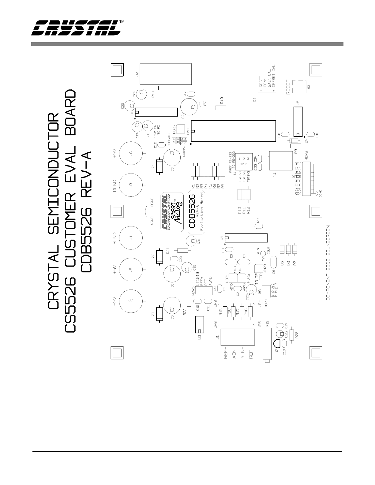
CDB5525 CDB5526
Figure 10. CDB5525/26 Component Side Silkscreen
44 DS202DB5
Page 45

CDB5525 CDB5526
Figure 11. CDB5525/26 Component Side (top)
DS202DB5 45
Page 46

CDB5525 CDB5526
Figure 12. CDB5525/26 Solder Side (bottom)
46 DS202DB5
Page 47

• Notes •
Page 48

 Loading...